qi-pc0-part12-v124.pdf
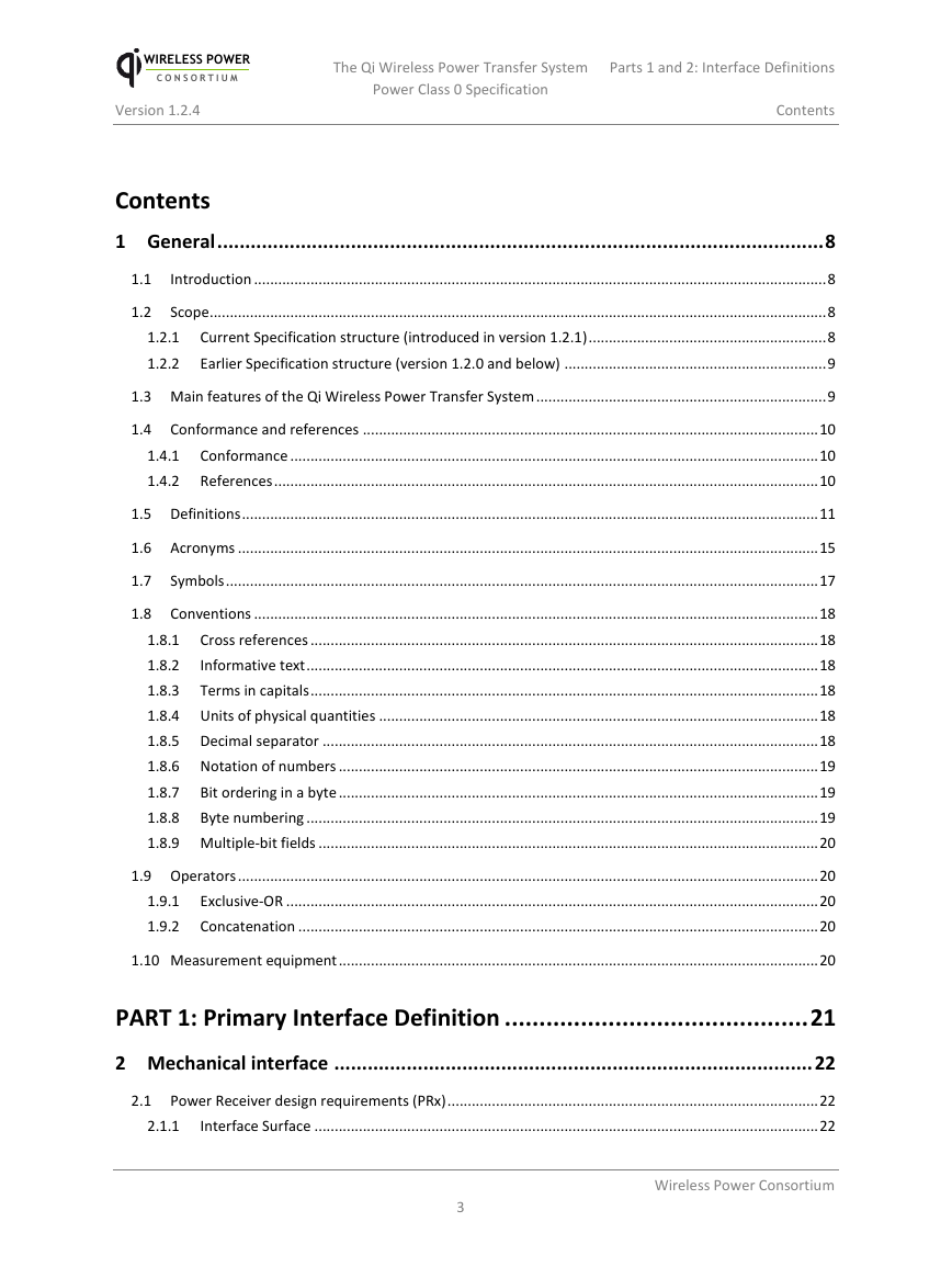
1 General
1.1 Introduction
1.2 Scope
1.2.1 Current Specification structure (introduced in version 1.2.1)
1.2.2 Earlier Specification structure (version 1.2.0 and below)
1.3 Main features of the Qi Wireless Power Transfer System
1.4 Conformance and references
1.4.1 Conformance
1.4.2 References
1.5 Definitions
1.6 Acronyms
1.7 Symbols
1.8 Conventions
1.8.1 Cross references
1.8.2 Informative text
1.8.3 Terms in capitals
1.8.4 Units of physical quantities
1.8.5 Decimal separator
1.8.6 Notation of numbers
1.8.7 Bit ordering in a byte
1.8.8 Byte numbering
1.8.9 Multiple-bit fields
1.9 Operators
1.9.1 Exclusive-OR
1.9.2 Concatenation
1.10 Measurement equipment
2 Mechanical interface
2.1 Power Receiver design requirements (PRx)
2.1.1 Interface Surface
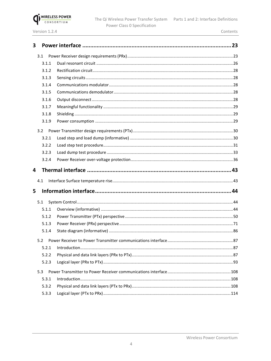
3 Power interface
3.1 Power Receiver design requirements (PRx)
3.1.1 Dual resonant circuit
3.1.2 Rectification circuit
3.1.3 Sensing circuits
3.1.4 Communications modulator
3.1.5 Communications demodulator
3.1.6 Output disconnect
3.1.7 Meaningful functionality
3.1.8 Shielding
3.1.9 Power consumption
3.2 Power Transmitter design requirements (PTx)
3.2.1 Load step and load dump (informative)
3.2.2 Load step test procedure
3.2.2.1 Baseline Power Profile load step test
3.2.2.2 Extended Power Profile load step test
3.2.3 Load dump test procedure
3.2.3.1 Baseline Power Profile load dump test
3.2.3.2 Extended Power Profile load dump test
3.2.4 Power Receiver over-voltage protection
4 Thermal interface
4.1 Interface Surface temperature rise
5 Information interface
5.1 System Control
5.1.1 Overview (informative)
5.1.1.1 Extended Power Profile
5.1.2 Power Transmitter (PTx) perspective
5.1.2.1 Selection phase (PTx perspective)
5.1.2.2 Ping phase (PTx perspective)
5.1.2.3 Identification & configuration phase (PTx perspective)
5.1.2.3.1 Creating a Power Transfer Contract
5.1.2.4 Negotiation phase—EPP only (PTx perspective)
5.1.2.4.1 Timing constraints
5.1.2.4.2 Actions associated with a request
5.1.2.4.2.1 Power Transmitter Responses
5.1.2.5 Calibration phase—EPP only (PTx perspective)
5.1.2.6 Power transfer phase (PTx perspective)
5.1.2.6.1 Power transfer control
5.1.2.7 Renegotiation phase—EPP only (PTx perspective)
5.1.3 Power Receiver (PRx) perspective
5.1.3.1 Selection phase (PRx perspective)
5.1.3.2 Ping phase (PRx perspective)
5.1.3.3 Identification & configuration phase (PRx perspective)
5.1.3.4 Negotiation phase—EPP only (PRx perspective)
5.1.3.4.1 Timing constraints
5.1.3.4.2 Actions associated with a request
5.1.3.4.2.1 Specific request
5.1.3.4.2.2 General request
5.1.3.4.2.3 FOD Status Packet
5.1.3.4.2.4 WPID Packets
5.1.3.4.2.5 Proprietary Packet
5.1.3.5 Calibration phase—EPP only (PRx perspective)
5.1.3.6 Power transfer phase (PRx perspective)
5.1.3.6.1 Communication requirements—EPP only
5.1.3.7 Renegotiation phase—EPP only (PRx perspective)
5.1.4 State diagram (informative)
5.2 Power Receiver to Power Transmitter communications interface
5.2.1 Introduction
5.2.2 Physical and data link layers (PRx to PTx)
5.2.2.1 Modulation scheme
5.2.2.2 Bit encoding scheme
5.2.2.3 Byte encoding scheme
5.2.2.4 Packet structure
5.2.2.4.1 Header
5.2.2.4.2 Message
5.2.2.4.3 Checksum
5.2.3 Logical layer (PRx to PTx)
5.2.3.1 Signal Strength Packet (0x01)
5.2.3.2 End Power Transfer Packet (0x02)
5.2.3.3 Control Error Packet (0x03)
5.2.3.4 8-bit Received Power Packet—BPP only (0x04)
5.2.3.5 Charge Status Packet (0x05)
5.2.3.6 Power Control Hold-off Packet (0x06)
5.2.3.7 Configuration Packet (0x51)
5.2.3.8 Identification Packet (0x71)
5.2.3.9 Wireless Power ID Packets (0x54 and 0x55)
5.2.3.9.1 CRC calculation
5.2.3.10 Extended Identification Packet (0x81)
5.2.3.11 24-bit Received Power Packet—EPP only (0x31)
5.2.3.12 General Request Packet—EPP only (0x07)
5.2.3.13 Specific Request Packet—EPP only (0x20)
5.2.3.13.1 End Negotiation (0x00)
5.2.3.13.2 Guaranteed Power (0x01)
5.2.3.13.3 Received Power Packet Type (0x02)
5.2.3.13.4 FSK Parameters (0x03)
5.2.3.13.5 Maximum Power (0x04)
5.2.3.14 FOD Status Packet—EPP only (0x22)
5.2.3.15 Renegotiate Packet—EPP only (0x09)
5.3 Power Transmitter to Power Receiver communications interface
5.3.1 Introduction
5.3.2 Physical and data link layers (PTx to PRx)
5.3.2.1 Modulation scheme
5.3.2.2 Bit encoding scheme
5.3.2.3 Packet structure
5.3.2.3.1 Byte encoding scheme
5.3.2.3.2 Header
5.3.2.3.3 Message
5.3.2.3.4 Checksum
5.3.2.4 Response structure
5.3.3 Logical layer (PTx to PRx)
5.3.3.1 Power Transmitter data not available Packet (0x00)
5.3.3.2 Power Transmitter Identification Packet (0x30)
5.3.3.3 Power Transmitter Capability Packet (0x31)
5.3.3.3.1 Example of power transfer process under normal conditions
5.3.3.3.2 Example of complete power transfer process with multiple events
6 External Power Input (Informative)
6.1 Available power—Extended Power Profile only
7 Power Levels—Extended Power Profile only
7.1 Guaranteed Power
7.2 Light load
8 System Efficiency (Informative)
8.1 Definition
8.2 Power Transmitter efficiency
8.2.1 Baseline Power Profile
8.2.2 Extended Power Profile
8.3 Power Receiver efficiency
9 Stand-by Power (Informative)
9.1 Transmitter Measurement Method
10 Object Detection (Informative)
10.1 Resonance shift
10.2 Capacitance change
11 Foreign Object Detection
11.1 Introduction
11.2 Baseline Power Profile
11.3 FOD based on quality factor change—EPP only
11.3.1 Q-factor measurement (Informative)
11.3.2 Expected operation (Informative)
11.3.3 Definition of the Reference Quality Factor
11.4 FOD based on calibrated power loss accounting—EPP only
11.4.1 Introduction
11.4.2 Received Power accuracy
11.4.3 Calibration
11.4.3.1 Calibrated Transmitted Power
11.4.3.2 Calibrated Received Power
11.5 FOD by Power Receiver (Informative)
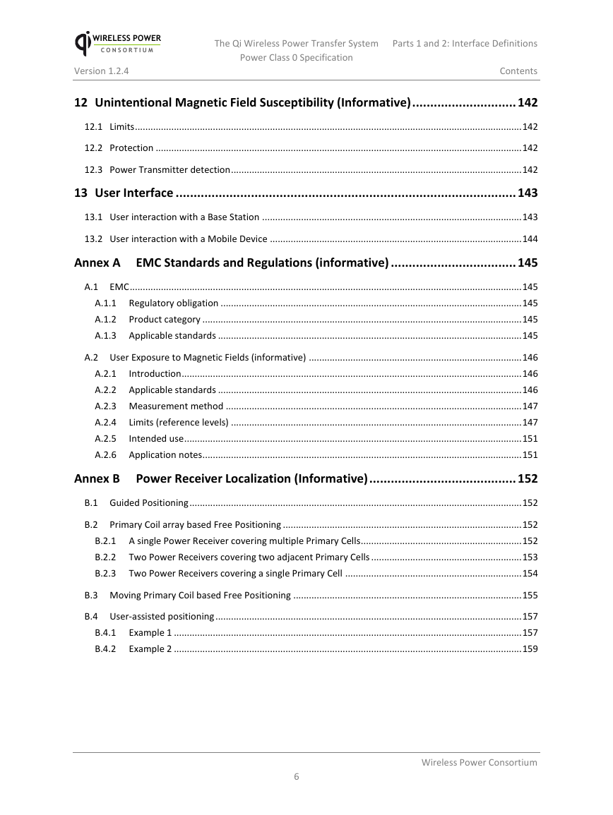
12 Unintentional Magnetic Field Susceptibility (Informative)
12.1 Limits
12.2 Protection
12.3 Power Transmitter detection
13 User Interface
13.1 User interaction with a Base Station
13.2 User interaction with a Mobile Device
Annex A EMC Standards and Regulations (informative)
A.1 EMC
A.1.1 Regulatory obligation
A.1.2 Product category
A.1.3 Applicable standards
A.2 User Exposure to Magnetic Fields (informative)
A.2.1 Introduction
A.2.2 Applicable standards
A.2.3 Measurement method
A.2.3.1 Magnetic field sensor
A.2.3.2 Measuring distance
A.2.4 Limits (reference levels)
A.2.4.1 Compliance criteria
A.2.4.2 Applicable limits
A.2.4.2.1 ICNIRP 1998
A.2.4.2.2 ICNIRP 2010
A.2.4.2.3 IEEE
A.2.5 Intended use
A.2.6 Application notes
Annex B Power Receiver Localization (Informative)
B.1 Guided Positioning
B.2 Primary Coil array based Free Positioning
B.2.1 A single Power Receiver covering multiple Primary Cells
B.2.2 Two Power Receivers covering two adjacent Primary Cells
B.2.3 Two Power Receivers covering a single Primary Cell
B.3 Moving Primary Coil based Free Positioning
B.4 User-assisted positioning
B.4.1 Example 1
B.4.2 Example 2
Annex C Power Receiver design guidelines (informative)
C.1 Large-signal resonance check
C.2 Power Receiver coil design
Annex D Mechanical Design Guidelines (Informative)
D.1 Base Station
D.2 Mobile Device
D.3 Base Station Alignment Aid
D.4 Mobile Device Alignment Aid
Annex E NFC/RFID card protection by the PTx (informative)
E.1 Introduction
E.2 Transmitter side NFC transceiver integration for tag protection
E.2.1 NFC antenna integration in a Power Transmitter
E.2.1.1 Design option 1: NFC antenna on top of the Primary Coil
E.2.1.2 Design option 2: NFC antenna outside the Primary Coil
E.2.1.3 Design option 3: NFC antenna on mainboard PCB
E.2.2 NFC transceiver integration
E.2.2.1 Using a separate NFC unit
E.2.2.2 Shared NFC processing
E.2.3 NFC polling
E.2.3.1 NFC polling loop in relation to power transfer phases
E.2.3.2 NFC Mobile Devices and tags
E.2.3.2.1 NFC Mobile Devices
E.2.3.2.2 Tags
E.2.3.3 NFC tag detection procedure and scenarios
E.2.3.3.1 Procedure
E.2.3.3.2 Scenario 1: one NMD (T4AT CEM) and one T4AT tag in the field
E.2.3.3.3 Scenario 2: one NMD and one T4BT tag in the field
E.2.3.3.4 Scenario 3: two tags in the field (one tag NFC-A and one tag NFC-B)
E.3 Optional object detection method using the NFC unit
E.3.1 Low power object detection in standby
E.3.2 Low power object detection in the power transfer phase
E.4 Test PICC for NFC unit emission level testing
E.4.1 Test PICC definition
E.4.2 Test PICC calibration
E.4.3 Test procedure using the test PICC
E.4.3.1 Test for analog & Digital Ping
E.4.3.2 Test for power transfer
Annex F History of Changes
qi-pc0-part3-v124
1 General
1.1 Introduction
1.2 Scope
1.2.1 Current Specification structure (introduced in version 1.2.1)
1.2.2 Earlier Specification structure (version 1.2.0 and below)
1.3 Main features of the Qi Wireless Power Transfer System
1.4 Conformance and references
1.4.1 Conformance
1.4.2 References
1.5 Definitions
1.6 Acronyms
1.7 Symbols
1.8 Conventions
1.8.1 Cross references
1.8.2 Informative text
1.8.3 Terms in capitals
1.8.4 Units of physical quantities
1.8.5 Decimal separator
1.8.6 Notation of numbers
1.8.7 Bit ordering in a byte
1.8.8 Byte numbering
1.8.9 Multiple-bit fields
1.9 Operators
1.9.1 Exclusive-OR
1.9.2 Concatenation
1.10 Measurement equipment
2 Compliance Testing Overview (Informative)
3 Specialized Base Station Testing Tools
3.1 Default Test Power Receiver configurations
3.1.1 Basic configuration for all TPRs
3.1.2 Additional configuration for regular FOD testing—version 1.1 TPRs
3.1.3 Additional configuration for the Extended Power Profile—version 1.2 TPRs
3.2 Test Power Receiver #1A
3.2.1 Operating range
3.3 Test Power Receiver #1B
3.3.1 Operating range
3.4 Test Power Receiver #1C
3.4.1 Operating range
3.5 Test Power Receiver #1D
3.5.1 Operating range
3.6 Test Power Receiver #1E
3.6.1 Operating range
3.7 Test Power Receiver #1F
3.8 Test Power Receiver #2—deprecated
3.9 Test Power Receiver #3
3.10 Test Power Receiver #4
3.11 Test Power Receiver #5
3.12 Test Power Receiver #6
3.12.1 Operating range
3.13 Test Power Receiver #7
3.14 Test Power Receivers #MP1A, #MP1B, and MP1C
3.14.1 Test Power Receiver #MP1A (8 W)
3.14.1.1 Operating range
3.14.2 Test Power Receiver #MP1B (15 W)
3.14.2.1 Operating range
3.14.3 Test Power Receiver #MP1C (12 W)
3.14.3.1 Operating range
3.15 Test Power Receiver #MP3
3.15.1 Operating range
3.16 Thermal Test Power Receivers
3.16.1 TPR-THERMAL-5W
3.16.1.1 Configuration
3.16.1.2 Operating point
3.16.2 TPR-THERMAL-15W
3.16.2.1 Operating point
3.17 Representative Foreign Objects
3.17.1 Thermocouple attachment
3.17.2 Frames and spacers
4 Specialized Mobile Device Testing Tools
4.1 Test Power Transmitter #1 (deprecated)
4.2 Test Power Transmitter #2
4.3 Test Power Transmitter #MP1
4.4 Test Power Transmitter–QFACTOR
5 Base Station Tests
5.1 Conformance to Power Transmitter designs
5.1.1 Magnet presence check
5.1.1.1 Required tools
5.1.1.2 Test configuration
5.1.1.3 Test procedure
5.1.1.4 Test results
5.2 Conformance to communications interface requirements
5.2.1 Load modulation
5.2.1.1 Required tools
5.2.1.2 Test configuration
5.2.1.3 Test procedure
5.2.1.4 Test results
5.2.2 Frequency modulation—MP.TX.COM.MOD
5.2.2.1 Required Tools
5.2.2.2 Test configuration
5.2.2.3 Test procedure
5.2.2.4 Test results
5.3 Conformance to system control requirements
5.3.1 Selection phase
5.3.1.1 Interface definition requirement
5.3.1.2 Required tools
5.3.1.3 Test configuration
5.3.1.4 Test procedure
5.3.1.5 Test results
5.3.2 Ping phase
5.3.2.1 Digital Ping: Power Signal characteristics
5.3.2.1.1 Interface definition requirement
5.3.2.1.2 Required tools
5.3.2.1.3 Test configuration
5.3.2.1.4 Test procedure
5.3.2.1.5 Test results
5.3.2.2 Digital Ping: no Response
5.3.2.2.1 Interface definition requirement
5.3.2.2.2 Required tools
5.3.2.2.3 Test configuration
5.3.2.2.4 Test procedure
5.3.2.2.5 Test results
5.3.2.3 Digital Ping: Signal Strength
5.3.2.3.1 Interface definition requirement
5.3.2.3.2 Required tools
5.3.2.3.3 Test configuration
5.3.2.3.4 Test procedure
5.3.2.3.5 Test results
5.3.2.4 Digital Ping: termination
5.3.2.4.1 Interface definition requirement
5.3.2.4.2 Required tools
5.3.2.4.3 Test configuration
5.3.2.4.4 Test procedure
5.3.2.4.5 Test results
5.3.3 Identification & configuration phase
5.3.3.1 Identification & configuration: Packet sequence
5.3.3.1.1 Interface definition requirement
5.3.3.1.2 Required tools
5.3.3.1.3 Test configuration
5.3.3.1.4 Test procedure
5.3.3.1.5 Test results
5.3.3.2 Identification & configuration: Packet timing
5.3.3.2.1 Interface definition requirement
5.3.3.2.2 Required tools
5.3.3.2.3 Test configuration
5.3.3.2.4 Test procedure
5.3.3.2.5 Test results
5.3.3.3 Identification & configuration: communication error
5.3.3.3.1 Interface definition requirement
5.3.3.3.2 Required tools
5.3.3.3.3 Test configuration
5.3.3.3.4 Test procedure
5.3.3.3.5 Test results
5.3.3.4 Identification & configuration: Packet content
5.3.3.4.1 Interface definition requirement
5.3.3.4.2 Required tools
5.3.3.4.3 Test configuration
5.3.3.4.4 Test procedure
5.3.3.4.5 Test results
5.3.3.5 Acknowledge negotiation request—MP.TX.SYSCTRL.IDCONFIG.ACK
5.3.3.5.1 Required tools
5.3.3.5.2 Test configuration
5.3.3.5.3 Test procedure
5.3.3.5.4 Test results
5.3.3.6 Identification & configuration: Power Transfer Contract
5.3.3.6.1 Interface definition requirement
5.3.3.6.2 Test results
5.3.4 Negotiation phase
5.3.4.1 Response to correctly transmitted Packets—MP.TX.SYSCTRL.NEG.RESPCOR
5.3.4.1.1 Required tools
5.3.4.1.2 Test configuration
5.3.4.1.3 Test procedure
5.3.4.1.4 Test results
5.3.4.2 Negotiation: Packet Response Timing—MP.TX.SYSCTRL.NEG.RESPTIME
5.3.4.2.1 Required tools
5.3.4.2.2 Test configuration
5.3.4.2.3 Test procedure
5.3.4.2.4 Test results
5.3.4.3 Negotiation: Remove Power—MP.TX.SYSCTRL.NEG.RMPOW
5.3.4.3.1 Required tools
5.3.4.3.2 Test configuration
5.3.4.3.3 Test procedure
5.3.4.3.4 Test results
5.3.4.4 Negotiation: End Negotiation—MP.TX.SYSCTRL.NEG.END
5.3.4.4.1 Required tools
5.3.4.4.2 Test configuration
5.3.4.4.3 Test procedure
5.3.4.4.4 Test results
5.3.4.5 Negotiation: Wireless Power ID—MP.TX.SYSCTRL.NEG.WPID
5.3.4.5.1 Performance requirement
5.3.4.5.2 Required tools
5.3.4.5.3 Test configuration
5.3.4.5.4 Test procedure
5.3.4.5.5 Test results
5.3.5 Power transfer phase
5.3.5.1 Power transfer: Packet sequence
5.3.5.1.1 Interface definition requirement
5.3.5.1.2 Required tools
5.3.5.1.3 Test configuration
5.3.5.1.4 Test procedure
5.3.5.1.5 Test results
5.3.5.2 Power transfer: Packet timing
5.3.5.2.1 Interface definition requirement
5.3.5.2.2 Required tools
5.3.5.2.3 Test configuration
5.3.5.2.4 Test procedure
5.3.5.2.5 Test results
5.3.5.3 Power transfer: Packet content
5.3.5.3.1 Interface definition requirement
5.3.5.3.2 Test results
5.3.5.4 Power transfer: power control
5.3.5.4.1 Interface definition requirement
5.3.5.4.2 Required tools
5.3.5.4.3 Test configuration
5.3.5.4.4 Test procedure
5.3.5.4.5 Test results
5.3.5.5 Power transfer: termination
5.3.5.5.1 Interface definition requirement
5.3.5.5.2 Required tools
5.3.5.5.3 Test configuration
5.3.5.5.4 Test procedure
5.3.5.5.5 Test results
5.3.5.6 Power transfer: renegotiation—MP.TX.SYSCTRL.POWXFER.RENEG
5.3.5.6.1 Required tools
5.3.5.6.2 Test configuration
5.3.5.6.3 Test procedure
5.3.5.6.4 Test results
5.4 Conformance to system performance requirements
5.4.1 Guaranteed power
5.4.1.1 Performance requirement
5.4.1.2 Required tools
5.4.1.3 Test configuration
5.4.1.4 Test procedure
5.4.1.5 Test results
5.4.2 Thermal Performance
5.4.2.1 Performance requirement
5.4.2.2 Required tools
5.4.2.3 Test configuration
5.4.2.4 Test procedure
5.4.2.5 Test results
5.4.3 Foreign Object detection
5.4.3.1 Object heating prevention
5.4.3.1.1 Performance requirement
5.4.3.1.2 Required tools
5.4.3.1.3 Test configuration
5.4.3.1.4 Test procedure
5.4.3.1.5 Test results
5.4.3.2 Heating prevention—MP.TX.PERF.FOD.MP
5.4.3.2.1 Test procedure
5.4.3.2.2 Test results
5.4.3.3 FOD before power transfer—MP.TX.FOD.BEFOREPOWER.FOD
5.4.3.3.1 Test procedure
5.4.3.3.2 Test results
5.4.3.4 FOD calibration—MP.TX.FOD.CALIBRATE.FO.ABSENT
5.4.3.4.1 Test procedure
5.4.3.4.2 Test results
5.4.3.5 FOD during power transfer—MP.TX.FOD.OPERATE.FOD
5.4.3.5.1 Test procedure
5.4.3.5.2 Test results
5.4.4 User interface: object placed
5.4.4.1 Performance requirement
5.4.4.2 Required tools
5.4.4.3 Test configuration
5.4.4.4 Test procedure
5.4.4.5 Test results
5.4.5 User interface: transfer in progress
5.4.5.1 Performance requirement
5.4.5.2 Required tools
5.4.5.3 Test configuration
5.4.5.4 Test procedure
5.4.5.5 Test results
5.4.6 User interface: transfer complete
5.4.6.1 Performance requirement
5.4.6.2 Required tools
5.4.6.3 Test configuration
5.4.6.4 Test procedure
5.4.6.5 Test results
5.4.7 User interface: fault
5.4.7.1 Performance requirement
5.4.7.2 Required tools
5.4.7.3 Test configuration
5.4.7.4 Test procedure
5.4.7.5 Test results
5.4.8 User interface: multiple devices
5.4.8.1 Performance requirement
5.4.8.2 Required tools
5.4.8.3 Test configuration
5.4.8.4 Test procedure
5.4.8.5 Test results
5.4.9 User interface: limited power
5.4.9.1 Performance requirement
5.4.9.2 Required tools
5.4.9.3 Test configuration
5.4.9.4 Test procedure
5.4.9.5 Test results
5.4.10 Maximum voltage
5.4.10.1 Required tools
5.4.10.2 Test configuration
5.4.10.3 Test procedure
5.4.10.4 Test results
5.4.11 Overvoltage protection
5.4.11.1 Required tools
5.4.11.2 Test configuration
5.4.11.3 Test procedure
5.4.11.4 Test result
6 Mobile Device Tests
6.1 Default Test Power Transmitter configurations
6.1.1 First default configuration for BPP and EPP MDUTs
6.1.2 Second default configuration for EPP MDUTs
6.2 Conformance to the Power Receiver design requirements
6.2.1 Interface Surface
6.2.1.1 Interface definition requirement
6.2.1.2 Test configuration
6.2.1.3 Test results
6.2.2 Alignment aid
6.2.2.1 Interface definition requirement
6.2.2.2 Test configuration
6.2.2.3 Test results
6.2.3 Dual resonant circuit
6.2.3.1 Interface definition requirement
6.2.3.2 Test configuration
6.2.3.3 Test results
6.2.4 Rectification circuit
6.2.4.1 Interface definition requirement
6.2.4.2 Test configuration
6.2.4.3 Test results
6.2.5 Sensing circuits
6.2.5.1 Interface definition requirement
6.2.5.2 Test configuration
6.2.5.3 Test results
6.2.6 Communications modulator
6.2.6.1 Interface definition requirement
6.2.6.2 Test configuration
6.2.6.3 Test results
6.2.7 Output disconnect switch
6.2.7.1 Interface definition requirement
6.2.7.2 Test configuration
6.2.7.3 Test results
6.3 Conformance to communications interface requirements
6.3.1 Load modulation
6.3.1.1 Interface definition requirement
6.3.1.2 Required tools
6.3.1.3 Test configuration
6.3.1.4 Test procedure
6.3.1.5 Test results
6.3.2 Frequency demodulation—MP.RX.COMMINTERF.FREQDEMOD
6.3.2.1 Required Tools
6.3.2.2 Test configuration
6.3.2.3 Test procedure
6.3.2.4 Test results
6.4 Conformance to system control requirements
6.4.1 Selection and ping phase
6.4.1.1 Digital Ping: Packet timing
6.4.1.1.1 Interface definition requirement
6.4.1.1.2 Required tools
6.4.1.1.3 Test configuration
6.4.1.1.4 Test procedure
6.4.1.1.5 Test results
6.4.1.2 Digital Ping: Packet content
6.4.1.2.1 Interface definition requirement
6.4.1.2.2 Required tools
6.4.1.2.3 Test configuration
6.4.1.2.4 Test procedure
6.4.1.2.5 Test results
6.4.1.3 Digital Ping: Signal Strength
6.4.1.3.1 Interface definition requirement
6.4.1.3.2 Required tools
6.4.1.3.3 Test configuration
6.4.1.3.4 Test procedure
6.4.1.3.5 Test results
6.4.2 Identification & configuration phase
6.4.2.1 Identification & configuration: Packet sequence
6.4.2.1.1 Interface definition requirement
6.4.2.1.2 Required tools
6.4.2.1.3 Test configuration
6.4.2.1.4 Test procedure
6.4.2.1.5 Test results
6.4.2.2 Identification & configuration: Packet timing
6.4.2.2.1 Interface definition requirement
6.4.2.2.2 Required tools
6.4.2.2.3 Test configuration
6.4.2.2.4 Test procedure
6.4.2.2.5 Test results
6.4.2.3 Identification & configuration: Packet content
6.4.2.3.1 Interface definition requirement
6.4.2.3.2 Required tools
6.4.2.3.3 Test configuration
6.4.2.3.4 Test procedure
6.4.2.3.5 Test results
6.4.3 Negotiation phase
6.4.3.1 Negotiation: Packet sequence—MP.RX.SYSCTRL.NEG.PACKSEQ
6.4.3.1.1 Required tools
6.4.3.1.2 Test configuration
6.4.3.1.3 Test procedure
6.4.3.1.4 Test results
6.4.3.2 Negotiation: Packet timing—MP.RX.SYSCTRL.NEG.PACKTIME
6.4.3.2.1 Required tools
6.4.3.2.2 Test configuration
6.4.3.2.3 Test procedure
6.4.3.2.4 Test results
6.4.3.3 Negotiation: Wireless Power ID—MP.RX.SYSCTRL.NEG.WPID
6.4.3.3.1 Required tools
6.4.3.3.2 Test Configuration
6.4.3.3.3 Test procedure
6.4.3.3.4 Test results
6.4.4 Power transfer phase
6.4.4.1 Power transfer: Packet sequence
6.4.4.1.1 Interface definition requirement
6.4.4.1.2 Required tools
6.4.4.1.3 Test configuration
6.4.4.1.4 Test procedure
6.4.4.1.5 Test results
6.4.4.2 Power transfer: Packet timing
6.4.4.2.1 Interface definition requirement
6.4.4.2.2 Required tools
6.4.4.2.3 Test configuration
6.4.4.2.4 Test procedure
6.4.4.2.5 Test results
6.4.4.3 Power transfer: Packet content
6.4.4.3.1 Interface definition requirement
6.4.4.3.2 Required tools
6.4.4.3.3 Test configuration
6.4.4.3.4 Test procedure
6.4.4.3.5 Test results
6.4.4.4 Power transfer Packet content—RX.SYSCTRL.POWXFER.PACKCONT
6.4.4.4.1 Required tools
6.4.4.4.2 Test configuration
6.4.4.4.3 Test procedure.
6.4.4.4.4 Test results
6.4.5 Power Receiver reset
6.4.5.1 Power Receiver: reset
6.4.5.1.1 Interface definition requirement
6.4.5.1.2 Required tools
6.4.5.1.3 Test configuration
6.4.5.1.4 Test procedure
6.4.5.1.5 Test results
6.5 Conformance to system performance requirements
6.5.1 Guaranteed power
6.5.1.1 Performance requirement
6.5.1.2 Required tools
6.5.1.3 Test configuration
6.5.1.4 Test procedure
6.5.1.5 Test results
6.5.2 FOD before power transfer—MP.RX.FOD.REQFODSTATUS
6.5.2.1 Required tools
6.5.2.2 Test procedure
6.5.2.3 Test results
6.5.3 FOD calibration—MP.RX.FOD.CALIBRATE
6.5.3.1 Required tools
6.5.3.2 Test Configuration
6.5.3.3 Test procedure
6.5.3.4 Test results
Annex A Construction of Test Power Receivers
A.1 Electronic circuit schematics of BPP Test Power Receivers
A.2 Mechanical construction of TPR#1A
A.3 Mechanical construction of TPR#1B
A.4 Mechanical construction of TPR#1C
A.5 Mechanical construction of TPR#1D
A.6 Mechanical construction of TPR#1E
A.7 Mechanical construction of TPR#2
A.8 Construction of TPR-THERMAL-5W
A.9 Construction of TPR-THERMAL-15W
Annex B Construction of a Test Power Transmitter
B.1 Electronic circuit schematics of TPT#2
B.2 Mechanical construction of TPT#2
Annex C Representative Foreign Objects (Normative)
C.1 Foreign Object #1
C.2 Foreign Object #2
C.3 Foreign Object #3
C.4 Foreign Object #4
Annex D History of Changes
qi-pc0-part4-v124
1 General
1.1 Introduction
1.2 Scope
1.2.1 Current Specification structure (introduced in version 1.2.1)
1.2.2 Earlier Specification structure (version 1.2.0 and below)
1.3 Main features
1.4 Conformance and references
1.4.1 Conformance
1.4.2 References
1.5 Definitions
1.6 Acronyms
1.7 Symbols
1.8 Conventions
1.8.1 Cross references
1.8.2 Informative text
1.8.3 Terms in capitals
1.8.4 Units of physical quantities
1.8.5 Decimal separator
1.8.6 Notation of numbers
1.8.7 Bit ordering in a byte
1.8.8 Byte numbering
1.8.9 Multiple-bit fields
1.9 Operators
1.9.1 Exclusive-OR
1.9.2 Concatenation
1.10 Measurement equipment
2 Power Transmitter reference designs
2.1 Introduction
2.2 Baseline Power Profile designs that activate a single Primary Coil at a time
2.2.1 Power Transmitter design A1
2.2.2 Power Transmitter design A2
2.2.2.1 Mechanical details
2.2.2.1.1 Primary Coil
2.2.2.1.2 Shielding
2.2.2.1.3 Interface Surface
2.2.2.1.4 Positioning stage
2.2.2.2 Electrical details
2.2.3 Power Transmitter design A3
2.2.3.1 Mechanical details
2.2.3.1.1 Primary Coil
2.2.3.1.2 Shielding
2.2.3.1.3 Interface Surface
2.2.3.1.4 Positioning stage
2.2.3.2 Electrical details
2.2.4 Power Transmitter design A4
2.2.4.1 Mechanical details
2.2.4.1.1 Primary Coil
2.2.4.1.2 Shielding
2.2.4.1.3 Interface Surface
2.2.4.1.4 Separation between multiple Power transmitters
2.2.4.2 Electrical details
2.2.5 Power Transmitter design A5
2.2.6 Power Transmitter design A6
2.2.6.1 Mechanical details
2.2.6.1.1 Primary Coil
2.2.6.1.2 Shielding
2.2.6.1.3 Interface Surface
2.2.6.1.4 Inter coil separation
2.2.6.2 Electrical details
2.2.7 Power Transmitter design A7
2.2.7.1 Mechanical details
2.2.7.1.1 Primary Coil
2.2.7.1.2 Shielding
2.2.7.1.3 Interface Surface
2.2.7.1.4 Positioning stage
2.2.7.2 Electrical details
2.2.8 Power Transmitter design A8
2.2.8.1 Mechanical details
2.2.8.1.1 Primary Coil
2.2.8.1.2 Shielding
2.2.8.1.3 Interface Surface
2.2.8.1.4 Separation between multiple Power transmitters
2.2.8.2 Electrical details
2.2.9 Power Transmitter design A9
2.2.10 Power Transmitter design A10
2.2.10.1 Mechanical details
2.2.10.1.1 Primary Coil
2.2.10.1.2 Shielding
2.2.10.1.3 Interface Surface
2.2.10.1.4 Alignment aid
2.2.10.1.5 Inter coil separation
2.2.10.2 Electrical details
2.2.11 Power Transmitter designs A11 and A11a
2.2.11.1 Power Transmitter design A11
2.2.11.1.1 Mechanical details
2.2.11.1.1.1 Primary Coil
2.2.11.1.1.2 Shielding
2.2.11.1.1.3 Interface Surface
2.2.11.1.1.4 Alignment aid
2.2.11.1.1.5 Inter coil separation
2.2.11.1.2 Electrical details
2.2.11.2 Power Transmitter design A11a
2.2.11.2.1 Mechanical details
2.2.11.2.1.1 Primary Coil
2.2.11.2.1.2 Shielding
2.2.11.2.1.3 Interface Surface
2.2.11.2.1.4 Alignment aid
2.2.11.2.1.5 Inter coil separation
2.2.11.2.2 Electrical details
2.2.12 Power Transmitter design A12
2.2.12.1 Mechanical details
2.2.12.1.1 Primary Coil
2.2.12.1.2 Shielding
2.2.12.1.3 Interface Surface
2.2.12.1.4 Inter coil separation
2.2.12.2 Electrical details
2.2.13 Power Transmitter design A13
2.2.13.1 Mechanical details
2.2.13.1.1 Primary Coil
2.2.13.1.2 Shielding
2.2.13.1.3 Interface Surface
2.2.13.1.4 Inter coil separation
2.2.13.2 Electrical details
2.2.14 Power Transmitter design A14
2.2.14.1 Mechanical details
2.2.14.1.1 Primary Coil
2.2.14.1.2 Shielding
2.2.14.1.3 Interface Surface
2.2.14.1.4 Inter coil separation
2.2.14.2 Electrical details
2.2.15 Power Transmitter design A15
2.2.15.1 Mechanical details
2.2.15.1.1 Primary Coil
2.2.15.1.2 Shielding
2.2.15.1.3 Interface Surface
2.2.15.1.4 Alignment aid
2.2.15.2 Electrical details
2.2.16 Power Transmitter design A16
2.2.16.1 Mechanical details
2.2.16.1.1 Primary Coil
2.2.16.1.2 Shielding
2.2.16.1.3 Interface Surface
2.2.16.1.4 Alignment aid
2.2.16.1.5 Inter coil separation
2.2.16.2 Electrical details
2.2.17 Power Transmitter design A17
2.2.17.1 Mechanical details
2.2.17.1.1 Primary Coil
2.2.17.1.2 Shielding
2.2.17.1.3 Interface Surface
2.2.17.1.4 Alignment aid
2.2.17.1.5 Inter coil separation
2.2.17.2 Electrical details
2.2.18 Power Transmitter design A18
2.2.18.1 Mechanical details
2.2.18.1.1 Primary Coil
2.2.18.1.2 Shielding
2.2.18.1.3 Interface Surface
2.2.18.1.4 Alignment aid
2.2.18.2 Electrical details
2.2.19 Power Transmitter design A19
2.2.19.1 Mechanical details
2.2.19.1.1 Primary Coil
2.2.19.1.2 Shielding
2.2.19.1.3 Interface Surface
2.2.19.1.4 Inter coil separation
2.2.19.2 Electrical details
2.2.20 Power Transmitter design A20
2.2.20.1 Mechanical details
2.2.20.1.1 Primary Coil
2.2.20.1.2 Shielding
2.2.20.1.3 Interface Surface
2.2.20.1.4 Separation between multiple Power transmitters
2.2.20.2 Electrical details
2.2.21 Power Transmitter design A21
2.2.21.1 Mechanical details
2.2.21.1.1 Primary Coil
2.2.21.1.2 Shielding
2.2.21.1.3 Interface Surface
2.2.21.1.4 Inter coil separation
2.2.21.2 Electrical details
2.2.22 Power Transmitter design A22
2.2.22.1 Mechanical details
2.2.22.1.1 Primary Coil
2.2.22.1.2 Shielding
2.2.22.1.3 Interface Surface
2.2.22.1.4 Separation between multiple Power transmitters
2.2.22.2 Electrical details
2.2.23 Power Transmitter design A23
2.2.23.1 Mechanical details
2.2.23.1.1 Primary Coil
2.2.23.1.2 Shielding
2.2.23.1.3 Interface Surface
2.2.23.1.4 Separation between multiple Power transmitters
2.2.23.2 Electrical details
2.2.24 Power Transmitter design A24
2.2.24.1 Mechanical details
2.2.24.1.1 Primary Coil
2.2.24.1.2 Shielding
2.2.24.1.3 Interface Surface
2.2.24.1.4 Separation between multiple Power transmitters
2.2.24.2 Electrical details
2.2.25 Power Transmitter design A25
2.2.25.1 Mechanical details
2.2.25.1.1 Primary Coil
2.2.25.1.2 Shielding
2.2.25.1.3 Interface Surface
2.2.25.1.4 Separation between multiple Power transmitters
2.2.25.2 Electrical details
2.2.26 Power Transmitter design A26
2.2.26.1 Mechanical details
2.2.26.1.1 Primary Coil
2.2.26.1.2 Shielding
2.2.26.1.3 Interface Surface
2.2.26.1.4 Alignment aid
2.2.26.1.5 Inter coil separation
2.2.26.2 Electrical details
2.2.27 Power Transmitter design A27
2.2.27.1 Mechanical details
2.2.27.1.1 Primary Coil
2.2.27.1.2 Shielding
2.2.27.1.3 Interface Surface
2.2.27.1.4 Alignment aid
2.2.27.1.5 Inter coil separation
2.2.27.2 Electrical details
2.2.28 Power Transmitter designs A28 and A28a
2.2.28.1 Power Transmitter design A28
2.2.28.1.1 Mechanical details
2.2.28.1.1.1 Primary Coil
2.2.28.1.1.2 Shielding
2.2.28.1.1.3 Interface Surface
2.2.28.1.1.4 Inter coil separation
2.2.28.1.2 Electrical details
2.2.28.2 Power Transmitter design A28a
2.2.28.2.1 Mechanical details
2.2.28.2.1.1 Primary Coil
2.2.28.2.1.2 Shielding
2.2.28.2.1.3 Interface Surface
2.2.28.2.1.4 Inter coil separation
2.2.28.2.2 Electrical details
2.2.29 Power Transmitter design A29
2.2.29.1 Mechanical details
2.2.29.1.1 Primary Coil
2.2.29.1.2 Shielding
2.2.29.1.3 Interface Surface
2.2.29.1.4 Alignment Aid
2.2.29.1.4.1 Inter coil separation
2.2.29.2 Electrical Details
2.2.30 Power Transmitter design A30
2.2.30.1 Mechanical details
2.2.30.1.1 Primary Coil
2.2.30.1.2 Shielding
2.2.30.1.3 Interface Surface
2.2.30.1.4 Separation between multiple Power transmitters
2.2.30.2 Electrical details
2.2.31 Power Transmitter design A31
2.2.31.1 Mechanical details
2.2.31.1.1 Primary Coil
2.2.31.1.2 Shielding
2.2.31.1.3 Interface Surface
2.2.31.1.4 Separation between multiple Power transmitters
2.2.31.2 Electrical details
2.2.32 Power Transmitter design A32
2.2.32.1 Mechanical details
2.2.32.1.1 Primary coil
2.2.32.1.2 Shielding
2.2.32.1.3 Interface Surface
2.2.32.1.4 Separation between multiple Power transmitters
2.2.32.2 Electrical details
2.2.33 Power Transmitter design A33
2.2.33.1 Mechanical details
2.2.33.1.1 Primary coil
2.2.33.1.2 Shielding
2.2.33.1.3 Interface Surface
2.2.33.1.4 Inter coil separation
2.2.33.2 Electrical details
2.2.34 Power Transmitter design A34
2.2.34.1 Mechanical details
2.2.34.1.1 Primary Coil
2.2.34.1.2 Shielding
2.2.34.1.3 Interface Surface
2.2.34.1.4 Inter coil separation
2.2.34.2 Electrical details
2.3 Baseline Power Profile designs that activate multiple Primary Coils simultaneously
2.3.1 Power Transmitter design B1
2.3.1.1 Mechanical details
2.3.1.1.1 Primary Coil array
2.3.1.1.2 Shielding
2.3.1.1.3 Interface Surface
2.3.1.2 Electrical details
2.3.1.3 Scalability
2.3.2 Power Transmitter design B2
2.3.2.1 Mechanical details
2.3.2.1.1 Primary Coil array
2.3.2.1.2 Shielding
2.3.2.1.3 Interface Surface
2.3.2.2 Electrical details
2.3.2.3 Scalability
2.3.3 Power Transmitter design B3
2.3.3.1 Mechanical details
2.3.3.1.1 Primary Coil array
2.3.3.1.2 Shielding
2.3.3.1.3 Interface Surface
2.3.3.2 Electrical details
2.3.3.3 Scalability
2.3.4 Power Transmitter design B4
2.3.4.1 Mechanical details
2.3.4.1.1 Primary Coil array
2.3.4.1.2 Shielding
2.3.4.1.3 Interface Surface
2.3.4.2 Electrical details
2.3.4.3 Scalability
2.3.5 Power Transmitter design B5
2.3.5.1 Mechanical details
2.3.5.1.1 Primary Coil array
2.3.5.1.2 Shielding
2.3.5.1.3 Interface Surface
2.3.5.2 Electrical details
2.3.5.3 Scalability
2.3.6 Power Transmitter design B6
2.3.6.1 Mechanical details
2.3.6.1.1 Primary Coil array
2.3.6.1.2 Shielding
2.3.6.1.3 Interface Surface
2.3.6.2 Electrical details
2.3.6.3 Scalability
2.3.7 Power Transmitter design B7
2.3.7.1 Mechanical details
2.3.7.1.1 Primary Coil array
2.3.7.1.2 Shielding
2.3.7.1.3 Interface Surface
2.3.7.2 Electrical details
2.3.7.3 Scalability
2.4 Extended Power Profile Power Transmitter designs
2.4.1 Power Transmitter design MP-A1
2.4.1.1 Mechanical details
2.4.1.1.1 Primary Coil
2.4.1.1.2 Shielding
2.4.1.1.3 Interface Surface
2.4.1.1.4 Alignment aid
2.4.1.1.5 Inter-coil separation
2.4.1.2 Electrical details
2.4.1.3 Information interface
2.4.2 Power Transmitter design MP-A2
2.4.2.1 Mechanical details
2.4.2.1.1 Primary Coil
2.4.2.1.2 Shielding
2.4.2.1.3 Interface Surface
2.4.2.1.4 Alignment aid
2.4.2.1.5 Inter-coil separation
2.4.2.2 Electrical details
2.4.2.3 Information interface
2.4.3 Power Transmitter design MP-A3
2.4.3.1 Mechanical details
2.4.3.1.1 Primary Coil
2.4.3.1.2 Shielding
2.4.3.1.3 Interface Surface
2.4.3.1.4 Inter-coil separation
2.4.3.2 Electrical details
2.4.3.3 Information interface
2.4.4 Power Transmitter design MP-A4
2.4.4.1 Mechanical details
2.4.4.1.1 Primary Coil
2.4.4.1.2 Shielding
2.4.4.1.3 Interface surface
2.4.4.1.4 Alignment aid
2.4.4.1.5 Inter-coil separation
2.4.4.2 Electrical details
2.4.4.3 Information interface
2.4.5 Power Transmitter design MP-A5
2.4.5.1 Mechanical details
2.4.5.1.1 Primary Coil
2.4.5.1.2 Shielding
2.4.5.1.3 Interface Surface
2.4.5.1.4 Alignment Aid
2.4.5.1.5 Inter coil separation
2.4.5.2 Electrical Details
2.4.5.3 Information interface
2.4.6 Power Transmitter design MP-A6
2.4.6.1 Mechanical details
2.4.6.1.1 Primary Coil
2.4.6.1.2 Shielding
2.4.6.1.3 Interface Surface
2.4.6.1.4 Alignment aid
2.4.6.1.5 Inter coil separation
2.4.6.2 Electrical details
2.4.6.3 Information interface
2.4.7 Power Transmitter design MP-A7
2.4.7.1 Mechanical details
2.4.7.1.1 Primary Coil
2.4.7.1.2 Shielding
2.4.7.1.3 Interface Surface
2.4.7.1.4 Alignment aid
2.4.7.1.5 Inter-coil separation
2.4.7.2 Electrical details
2.4.7.3 Information interface
2.4.8 Power Transmitter design MP-A8
2.4.8.1 Mechanical details
2.4.8.1.1 Primary Coil
2.4.8.1.2 Shielding
2.4.8.1.3 Interface Surface
2.4.8.1.4 Alignment aid
2.4.8.1.5 Inter-coil separation
2.4.8.2 Electrical details
2.4.8.3 Information interface
2.4.9 Power Transmitter design MP-A9
2.4.9.1 Mechanical details
2.4.9.1.1 Primary Coil
2.4.9.1.2 Shielding
2.4.9.1.3 Interface Surface
2.4.9.1.4 Alignment aid
2.4.9.1.5 Inter-coil separation
2.4.9.2 Electrical details
2.4.9.3 Information Interface
2.4.10 Power Transmitter design MP-A10
2.4.10.1 Mechanical details
2.4.10.1.1 Primary Coil
2.4.10.1.2 Shielding
2.4.10.1.3 Interface Surface
2.4.10.1.4 Alignment aid
2.4.10.1.5 Inter coil separation
2.4.10.2 Electrical details
2.4.10.3 Information interface
2.4.11 Power Transmitter design MP-A13
2.4.11.1 Mechanical details
2.4.11.1.1 Primary Coil
2.4.11.1.2 Shielding
2.4.11.1.3 Interface Surface
2.4.11.1.4 Alignment aid
2.4.11.1.5 Inter coil separation
2.4.11.2 Electrical details
2.4.11.3 Information interface
2.4.12 Power Transmitter design MP-B1
2.4.12.1 Mechanical details
2.4.12.1.1 Primary Coil array
2.4.12.1.2 Shielding
2.4.12.1.3 Interface Surface
2.4.12.2 Electrical details
2.4.12.3 Scalability
3 Power Receiver reference designs (Informative)
3.1 Power Receiver example 1 (5W)
3.1.1 Mechanical details
3.1.1.1 Secondary Coil
3.1.1.2 Shielding
3.1.1.3 Interface Surface
3.1.1.4 Alignment aid
3.1.2 Electrical details
3.2 Power Receiver example 2 (5W)
3.2.1 Mechanical details
3.2.1.1 Secondary Coil
3.2.1.2 Shielding
3.2.1.3 Interface Surface
3.2.1.4 Alignment aid
3.2.2 Electrical details
3.3 Power Receiver example 3 (8 W)
3.3.1 Mechanical details
3.3.1.1 Secondary Coil
3.3.1.2 Shielding
3.3.1.3 Interface Surface
3.3.1.4 Alignment aid
3.3.2 Electrical details
3.4 Power Receiver example 4 (15 W)
3.4.1 Mechanical details
3.4.1.1 Secondary Coil
3.4.1.2 Shielding
3.4.1.3 Interface Surface
3.4.1.4 Alignment aid
3.4.2 Electrical details
3.5 Power Receiver example 5 (12 W)
3.5.1 Mechanical details
3.5.1.1 Secondary Coil
3.5.1.2 Shielding
3.5.1.3 Interface Surface
3.5.2 Electrical details
Annex A History of Changes




 2023年江西萍乡中考道德与法治真题及答案.doc
 2012年重庆南川中考生物真题及答案.doc
 2013年江西师范大学地理学综合及文艺理论基础考研真题.doc
 2020年四川甘孜小升初语文真题及答案I卷.doc
 2020年注册岩土工程师专业基础考试真题及答案.doc
 2023-2024学年福建省厦门市九年级上学期数学月考试题及答案.doc
 2021-2022学年辽宁省沈阳市大东区九年级上学期语文期末试题及答案.doc
 2022-2023学年北京东城区初三第一学期物理期末试卷及答案.doc
 2018上半年江西教师资格初中地理学科知识与教学能力真题及答案.doc
 2012年河北国家公务员申论考试真题及答案-省级.doc
 2020-2021学年江苏省扬州市江都区邵樊片九年级上学期数学第一次质量检测试题及答案.doc
 2022下半年黑龙江教师资格证中学综合素质真题及答案.doc