Sitara™ AM335x ARM® Cortex™-A8
Microprocessors (MPUs)
Silicon Revisions 2.1, 2.0, 1.0
Silicon Errata
Literature Number: SPRZ360F
October 2011–Revised November 2013
�
Contents
1
2
3
3.2
3.1
1.1
1.2
Introduction ........................................................................................................................ 3
AM335x Device and Development Support Tool Nomenclature .................................................. 3
Revision Identification ................................................................................................... 4
All Errata Listed With Silicon Revision Number ...................................................................... 6
Usage Notes and Known Design Exceptions to Functional Specifications ................................. 8
Usage Notes ............................................................................................................. 8
LCD: Color Assignments of LCD_DATA Terminals ..................................................... 8
3.1.1
DDR3: JEDEC Compliance for Maximum Self-Refresh Command Limit ............................ 8
3.1.2
Boot: USB Boot ROM Code Uses Default DATAPOLARITY .......................................... 9
3.1.3
Boot: Multiplexed Signals GPMC_WAIT0, GMII2_CRS, and RMII2_CRS_DV Cause NAND Boot
3.1.4
Issue ........................................................................................................... 9
Pin Multiplexing: Valid IO Sets and Restrictions ....................................................... 10
3.1.5
Boot: Multiplexed Signals GPMC_WAIT0 and GMII2_CRS Cause NAND Boot Issue ........... 10
3.1.6
OSC1: RTC_XTALIN Terminal Has an Internal Pull-up Resistor When OSC1 is Disabled ...... 11
3.1.7
Known Design Exceptions to Functional Specifications .......................................................... 12
Revision History ......................................................................................................................... 38
2
Table of Contents
Copyright © 2011–2013, Texas Instruments Incorporated
SPRZ360F–October 2011–Revised November 2013
Submit Documentation Feedback
�
Silicon Errata
SPRZ360F–October 2011–Revised November 2013
Sitara™ AM335x ARM® Cortex™-A8
Microprocessors (MPUs)
(Silicon Revision 2.1, 2.0, 1.0)
1
Introduction
This document describes the known exceptions to the functional specifications for the Sitara™ AM335x
ARM® Cortex™-A8 Microprocessors (MPUs). [See the Sitara AM335x ARM Cortex-A8 Microprocessors
(MPUs) data manual (literature number SPRS717).]
For additional information, see the latest version of the Sitara AM335x ARM Cortex-A8 Microprocessors
(MPUs) Technical Reference Manual (literature number SPRUH73).
1.1 AM335x Device and Development Support Tool Nomenclature
To designate the stages in the product development cycle, TI assigns prefixes to the part numbers of all
microprocessors (MPUs) and support tools. Each device has one of three prefixes: X, P, or null (no prefix)
(for example, XAM3358ZCE). Texas Instruments recommends two of three possible prefix designators for
its support tools: TMDX and TMDS. These prefixes represent evolutionary stages of product development
from engineering prototypes (TMDX) through fully qualified production devices and tools (TMDS).
Device development evolutionary flow:
X — Experimental device that is not necessarily representative of the final device's electrical
specifications and may not use production assembly flow.
P — Prototype device that is not necessarily the final silicon die and may not necessarily meet final
electrical specifications.
null — Production version of the silicon die that is fully qualified.
Support tool development evolutionary flow:
TMDX — Development-support product that has not yet completed Texas Instruments internal
qualification testing.
TMDS — Fully-qualified development-support product.
X and P devices and TMDX development-support tools are shipped against the following disclaimer:
"Developmental product is intended for internal evaluation purposes."
Production devices and TMDS development-support tools have been characterized fully, and the quality
and reliability of the device have been demonstrated fully. TI's standard warranty applies.
Predictions show that prototype devices (X or P) have a greater failure rate than the standard production
devices. Texas Instruments recommends that these devices not be used in any production system
because their expected end-use failure rate still is undefined. Only qualified production devices are to be
used.
Sitara is a trademark of Texas Instruments.
Cortex is a trademark of ARM Ltd or its subsidiaries.
ARM is a registered trademark of ARM Ltd or its subsidiaries.
All other trademarks are the property of their respective owners.
SPRZ360F–October 2011–Revised November 2013
Submit Documentation Feedback
Copyright © 2011–2013, Texas Instruments Incorporated
Sitara™ AM335x ARM® Cortex™-A8 Microprocessors (MPUs) (Silicon
Revision 2.1, 2.0, 1.0)
3
�
Introduction
1.2 Revision Identification
www.ti.com
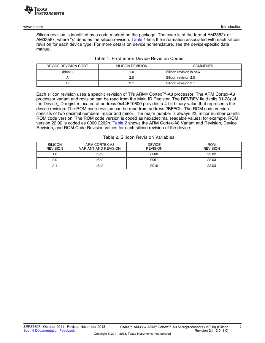
The device revision can be determined by the symbols marked on the top of the package. Figure 1
provides an example of the AM335x device markings.
Figure 1. Example of Device Revision Codes for the AM335x Microprocessor
NOTES:
(A) Non-qualified devices are marked with the letters "X" or "P" at the beginning of the device name, while
qualified devices have a "blank" at the beginning of the device name.
(B) The AM3352 and AM3359 devices shown in this device marking example are two of several valid part
numbers for the AM335x family of devices.
(C) The device revision code is the device revision (A, B, and so on).
(D) YM denotes year and month.
(E) LLLL denotes Lot Trace Code.
(F) 962 is a generic family marking ID.
(G) G1 denotes green, lead-free.
(H) ZCE or ZCZ is the package designator.
(I) S denotes Assembly Site Code.
(J) On some "X" devices, the device speed may not be shown.
4
Sitara™ AM335x ARM® Cortex™-A8 Microprocessors (MPUs) (Silicon
Revision 2.1, 2.0, 1.0)
Copyright © 2011–2013, Texas Instruments Incorporated
SPRZ360F–October 2011–Revised November 2013
Submit Documentation Feedback
Lot Trace CodeXAM3352AZCEYMLLLLS962ZCEG1Device RevisionLot Trace CodeXAM3359AZCZYMLLLLS962ZCZG1Device Revision�
www.ti.com
Introduction
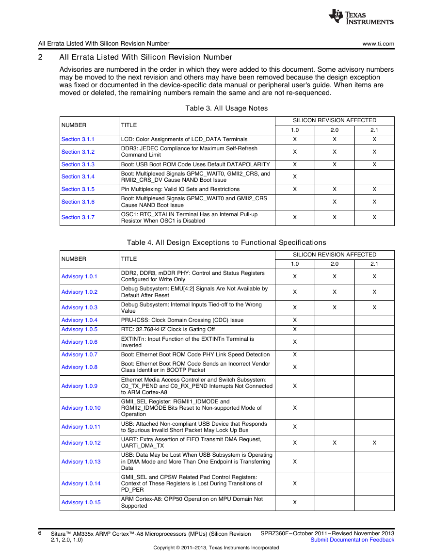
Silicon revision is identified by a code marked on the package. The code is of the format AM3352x or
AM3358x, where "x" denotes the silicon revision. Table 1 lists the information associated with each silicon
revision for each device type. For more details on device nomenclature, see the device-specific data
manual.
DEVICE REVISION CODE
SILICON REVISION
COMMENTS
Table 1. Production Device Revision Codes
(blank)
A
B
1.0
2.0
2.1
Silicon revision is new
Silicon revision 2.0
Silicon revision 2.1
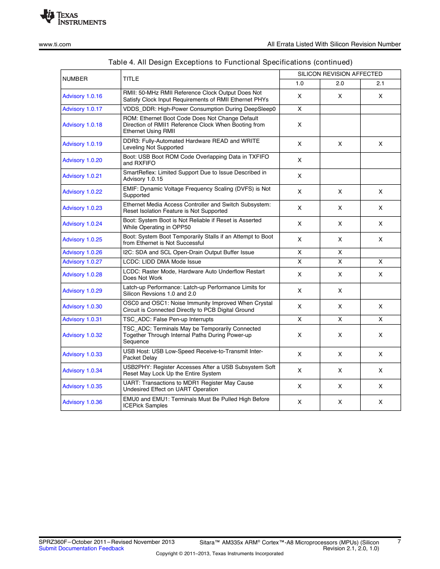
Each silicon revision uses a specific revision of TI's ARM® Cortex™-A8 processor. The ARM Cortex-A8
processor variant and revision can be read from the Main ID Register. The DEVREV field (bits 31-28) of
the Device_ID register located at address 0x44E10600 provides a 4-bit binary value that represents the
device revision. The ROM code revision can be read from address 2BFFCh. The ROM code version
consists of two decimal numbers: major and minor. The major number is always 22, minor number counts
ROM code version. The ROM code version is coded as hexadecimal readable values; for example, ROM
version 22.02 is coded as 0000 2202h. Table 2 shows the ARM Cortex-A8 Variant and Revision, Device
Revision, and ROM Code Revision values for each silicon revision of the device.
Table 2. Silicon Revision Variables
SILICON
REVISION
ARM CORTEX-A8
VARIANT AND REVISION
1.0
2.0
2.1
r3p2
r3p2
r3p2
DEVICE
REVISION
0000
0001
0010
ROM
REVISION
22.02
22.03
22.03
SPRZ360F–October 2011–Revised November 2013
Submit Documentation Feedback
Copyright © 2011–2013, Texas Instruments Incorporated
Sitara™ AM335x ARM® Cortex™-A8 Microprocessors (MPUs) (Silicon
Revision 2.1, 2.0, 1.0)
5
�
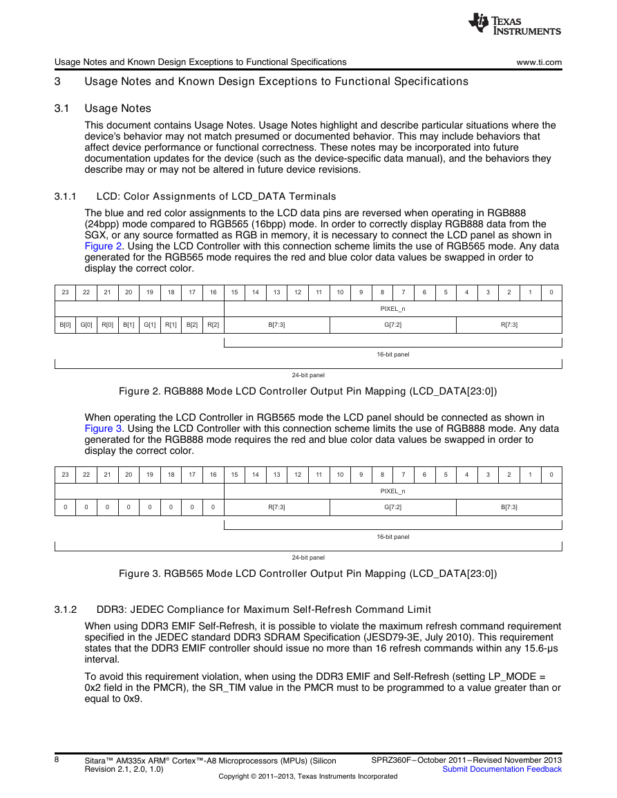
All Errata Listed With Silicon Revision Number
2
All Errata Listed With Silicon Revision Number
Advisories are numbered in the order in which they were added to this document. Some advisory numbers
may be moved to the next revision and others may have been removed because the design exception
was fixed or documented in the device-specific data manual or peripheral user's guide. When items are
moved or deleted, the remaining numbers remain the same and are not re-sequenced.
www.ti.com
Table 3. All Usage Notes
NUMBER
TITLE
Section 3.1.1
Section 3.1.2
Section 3.1.3
Section 3.1.4
Section 3.1.5
Section 3.1.6
Section 3.1.7
LCD: Color Assignments of LCD_DATA Terminals
DDR3: JEDEC Compliance for Maximum Self-Refresh
Command Limit
Boot: USB Boot ROM Code Uses Default DATAPOLARITY
Boot: Multiplexed Signals GPMC_WAIT0, GMII2_CRS, and
RMII2_CRS_DV Cause NAND Boot Issue
Pin Multiplexing: Valid IO Sets and Restrictions
Boot: Multiplexed Signals GPMC_WAIT0 and GMII2_CRS
Cause NAND Boot Issue
OSC1: RTC_XTALIN Terminal Has an Internal Pull-up
Resistor When OSC1 is Disabled
SILICON REVISION AFFECTED
1.0
2.1
X
X
2.0
X
X
X
X
X
X
X
X
X
X
X
X
X
X
X
X
Table 4. All Design Exceptions to Functional Specifications
NUMBER
TITLE
SILICON REVISION AFFECTED
1.0
2.1
2.0
Advisory 1.0.1
Advisory 1.0.2
Advisory 1.0.3
Advisory 1.0.4
Advisory 1.0.5
Advisory 1.0.6
Advisory 1.0.7
Advisory 1.0.8
Advisory 1.0.9
Advisory 1.0.10
Advisory 1.0.11
Advisory 1.0.12
Advisory 1.0.13
Advisory 1.0.14
Advisory 1.0.15
DDR2, DDR3, mDDR PHY: Control and Status Registers
Configured for Write Only
Debug Subsystem: EMU[4:2] Signals Are Not Available by
Default After Reset
Debug Subsystem: Internal Inputs Tied-off to the Wrong
Value
PRU-ICSS: Clock Domain Crossing (CDC) Issue
RTC: 32.768-kHZ Clock is Gating Off
EXTINTn: Input Function of the EXTINTn Terminal is
Inverted
Boot: Ethernet Boot ROM Code PHY Link Speed Detection
Boot: Ethernet Boot ROM Code Sends an Incorrect Vendor
Class Identifier in BOOTP Packet
Ethernet Media Access Controller and Switch Subsystem:
C0_TX_PEND and C0_RX_PEND Interrupts Not Connected
to ARM Cortex-A8
GMII_SEL Register: RGMII1_IDMODE and
RGMII2_IDMODE Bits Reset to Non-supported Mode of
Operation
USB: Attached Non-compliant USB Device that Responds
to Spurious Invalid Short Packet May Lock Up Bus
UART: Extra Assertion of FIFO Transmit DMA Request,
UARTi_DMA_TX
USB: Data May be Lost When USB Subsystem is Operating
in DMA Mode and More Than One Endpoint is Transferring
Data
GMII_SEL and CPSW Related Pad Control Registers:
Context of These Registers is Lost During Transitions of
PD_PER
ARM Cortex-A8: OPP50 Operation on MPU Domain Not
Supported
X
X
X
X
X
X
X
X
X
X
X
X
X
X
X
X
X
X
X
X
X
X
X
6
Sitara™ AM335x ARM® Cortex™-A8 Microprocessors (MPUs) (Silicon Revision
2.1, 2.0, 1.0)
SPRZ360F–October 2011–Revised November 2013
Submit Documentation Feedback
Copyright © 2011–2013, Texas Instruments Incorporated
�
www.ti.com
All Errata Listed With Silicon Revision Number
Table 4. All Design Exceptions to Functional Specifications (continued)
NUMBER
TITLE
SILICON REVISION AFFECTED
1.0
2.1
2.0
Advisory 1.0.16
Advisory 1.0.17
Advisory 1.0.18
Advisory 1.0.19
Advisory 1.0.20
Advisory 1.0.21
Advisory 1.0.22
Advisory 1.0.23
Advisory 1.0.24
Advisory 1.0.25
Advisory 1.0.26
Advisory 1.0.27
Advisory 1.0.28
Advisory 1.0.29
Advisory 1.0.30
Advisory 1.0.31
Advisory 1.0.32
Advisory 1.0.33
Advisory 1.0.34
Advisory 1.0.35
Advisory 1.0.36
RMII: 50-MHz RMII Reference Clock Output Does Not
Satisfy Clock Input Requirements of RMII Ethernet PHYs
VDDS_DDR: High-Power Consumption During DeepSleep0
ROM: Ethernet Boot Code Does Not Change Default
Direction of RMII1 Reference Clock When Booting from
Ethernet Using RMII
DDR3: Fully-Automated Hardware READ and WRITE
Leveling Not Supported
Boot: USB Boot ROM Code Overlapping Data in TXFIFO
and RXFIFO
SmartReflex: Limited Support Due to Issue Described in
Advisory 1.0.15
EMIF: Dynamic Voltage Frequency Scaling (DVFS) is Not
Supported
Ethernet Media Access Controller and Switch Subsystem:
Reset Isolation Feature is Not Supported
Boot: System Boot is Not Reliable if Reset is Asserted
While Operating in OPP50
Boot: System Boot Temporarily Stalls if an Attempt to Boot
from Ethernet is Not Successful
I2C: SDA and SCL Open-Drain Output Buffer Issue
LCDC: LIDD DMA Mode Issue
LCDC: Raster Mode, Hardware Auto Underflow Restart
Does Not Work
Latch-up Performance: Latch-up Performance Limits for
Silicon Revsions 1.0 and 2.0
OSC0 and OSC1: Noise Immunity Improved When Crystal
Circuit is Connected Directly to PCB Digital Ground
TSC_ADC: False Pen-up Interrupts
TSC_ADC: Terminals May be Temporarily Connected
Together Through Internal Paths During Power-up
Sequence
USB Host: USB Low-Speed Receive-to-Transmit Inter-
Packet Delay
USB2PHY: Register Accesses After a USB Subsystem Soft
Reset May Lock Up the Entire System
UART: Transactions to MDR1 Register May Cause
Undesired Effect on UART Operation
EMU0 and EMU1: Terminals Must Be Pulled High Before
ICEPick Samples
X
X
X
X
X
X
X
X
X
X
X
X
X
X
X
X
X
X
X
X
X
X
X
X
X
X
X
X
X
X
X
X
X
X
X
X
X
X
X
X
X
X
X
X
X
X
X
X
X
X
X
X
X
SPRZ360F–October 2011–Revised November 2013
Submit Documentation Feedback
Copyright © 2011–2013, Texas Instruments Incorporated
Sitara™ AM335x ARM® Cortex™-A8 Microprocessors (MPUs) (Silicon
Revision 2.1, 2.0, 1.0)
7
�
Usage Notes and Known Design Exceptions to Functional Specifications
3
Usage Notes and Known Design Exceptions to Functional Specifications
www.ti.com
3.1 Usage Notes
This document contains Usage Notes. Usage Notes highlight and describe particular situations where the
device's behavior may not match presumed or documented behavior. This may include behaviors that
affect device performance or functional correctness. These notes may be incorporated into future
documentation updates for the device (such as the device-specific data manual), and the behaviors they
describe may or may not be altered in future device revisions.
3.1.1
LCD: Color Assignments of LCD_DATA Terminals
The blue and red color assignments to the LCD data pins are reversed when operating in RGB888
(24bpp) mode compared to RGB565 (16bpp) mode. In order to correctly display RGB888 data from the
SGX, or any source formatted as RGB in memory, it is necessary to connect the LCD panel as shown in
Figure 2. Using the LCD Controller with this connection scheme limits the use of RGB565 mode. Any data
generated for the RGB565 mode requires the red and blue color data values be swapped in order to
display the correct color.
Figure 2. RGB888 Mode LCD Controller Output Pin Mapping (LCD_DATA[23:0])
When operating the LCD Controller in RGB565 mode the LCD panel should be connected as shown in
Figure 3. Using the LCD Controller with this connection scheme limits the use of RGB888 mode. Any data
generated for the RGB888 mode requires the red and blue color data values be swapped in order to
display the correct color.
Figure 3. RGB565 Mode LCD Controller Output Pin Mapping (LCD_DATA[23:0])
3.1.2
DDR3: JEDEC Compliance for Maximum Self-Refresh Command Limit
When using DDR3 EMIF Self-Refresh, it is possible to violate the maximum refresh command requirement
specified in the JEDEC standard DDR3 SDRAM Specification (JESD79-3E, July 2010). This requirement
states that the DDR3 EMIF controller should issue no more than 16 refresh commands within any 15.6-μs
interval.
To avoid this requirement violation, when using the DDR3 EMIF and Self-Refresh (setting LP_MODE =
0x2 field in the PMCR), the SR_TIM value in the PMCR must to be programmed to a value greater than or
equal to 0x9.
8
Sitara™ AM335x ARM® Cortex™-A8 Microprocessors (MPUs) (Silicon
Revision 2.1, 2.0, 1.0)
Copyright © 2011–2013, Texas Instruments Incorporated
SPRZ360F–October 2011–Revised November 2013
Submit Documentation Feedback
23222120191817161514131211109876543210PIXEL_n00000000R[7:3]G[7:2]B[7:3]16-bit panel24-bit panel23222120191817161514131211109876543210PIXEL_nB[0]G[0]R[0]B[1]G[1]R[1]B[2]R[2]B[7:3]G[7:2]R[7:3]16-bit panel24-bit panel�


 2023年江西萍乡中考道德与法治真题及答案.doc
 2012年重庆南川中考生物真题及答案.doc
 2013年江西师范大学地理学综合及文艺理论基础考研真题.doc
 2020年四川甘孜小升初语文真题及答案I卷.doc
 2020年注册岩土工程师专业基础考试真题及答案.doc
 2023-2024学年福建省厦门市九年级上学期数学月考试题及答案.doc
 2021-2022学年辽宁省沈阳市大东区九年级上学期语文期末试题及答案.doc
 2022-2023学年北京东城区初三第一学期物理期末试卷及答案.doc
 2018上半年江西教师资格初中地理学科知识与教学能力真题及答案.doc
 2012年河北国家公务员申论考试真题及答案-省级.doc
 2020-2021学年江苏省扬州市江都区邵樊片九年级上学期数学第一次质量检测试题及答案.doc
 2022下半年黑龙江教师资格证中学综合素质真题及答案.doc