INSPIRE
18218088355 Q463449374
STL6288
Ultralow Power NTSC/PAL Video Decoder
Data Manual
March 2016
V1.0
18218088355 Q463449374
�
STL6288 INSPIRE
18218088355 Q463449374
STL6288
Ultralow Power NTSC/PAL Video Decoder
Introduction
1
The STL6288 device is an ultralow power NTSC/PAL/ video decoder. Available in
a space saving 32pin QFN package, the STL6288 decoder converts NTSC and PAL
video signals to 8-bit ITU-R BT.656 format. Discrete syncs are also available. The
optimized architecture of the STL6288 decoder allows for ultralow-power
consumption. The decoder uses just one crystal for all supported standards, or any
frequency between 10 MHz and 50MHz. The STL6288 decoder can be
programmed using an I2C serial interface. The decoder uses a 1.8V supply for its
analog and digital supplies, and a 3.3Vor 1.8V supply for its I/O.
The STL6288 decoder converts baseband analog video into digital YCbCr 4:2:2
component video. Composite and S-video inputs are supported. The STL6288
decoder includes one 9-bit analog-to-digital converter (ADC) with 2x sampling.
Sampling is ITU-R BT.601 (27.0 MHz, generated from the 14.31818-MHz crystal
or oscillator input) and is line-locked. The output formats can be 8-bit 4:2:2 or 8-bit
ITU-R BT.656 with embedded synchronization.
2 Features
a) High-speed 30MSPS 9-bit ADC
b) Accepts NTSC (M,J,4.43), PAL (B, D, G, H, I, M, N, NC) video data
c) Two composite inputs or one S-video input
d) Brightness, contrast, saturation, hue, and sharpness control through I2C
e) Standard programmable video output format:
-ITU-R BT.656, 8-bit 4:2:2 with embedded syncs
-8bit 4:2:2 ITU-R BT.601 with discrete syncs
f) programmable output position and windth of HSYNC,VSYNC and FID
g) Patented Architecture for Locking to Weak, Noisy, or Unstable Signals
h) Internal phase-locked loop (PLL) for line-locked clock and sampling
i) Wide frequency Input from 10MHz to 50MHz
j) Power-on reset
k) 32pin QFN package.
l) 3.3Vor 1.8V supply for its I/O
3 Ordering Information
Part Number
STL688
4 Terminal Assignments
The STL6288 video decoder bridge is packaged in a 32-terminal QFN package.
Figure 1 shows the terminal diagram for the packages. Table 1 gives a description
of the terminals.
Package
QFN32
Package Option
Reel
1
�
Ultralow Power NTSC/PAL Video Decoder STL6288
Q463449374
Fig. 1 STL628 Terminal Diagrams ( Top View )
Tab. 1 Terminal Functions
TERMINAL
NAME
Analog Section
AGND
AIP1A
AIP1B
CH_AGND
CH_AVDD
PLL_AGND
PLL_AVDD
REFM
REFP
I/O
NO.
DESCRIPTION
7
1
2
31
32
3
4
30
29
I
I
I
I
I
I
I
I
I
Substrate. Connect to analog ground.
Analog input. Connect to the video analog input via
0.1µF capacitor. The maximum input range is 0-0.75
VPP, and may require an attenuator to reduce the
input amplitude to the desired level. If not used,
connect to AGND via a 0.1µF capacitor.
Analog input. Connect to the video analog input via
0.1µF capacitor. The maximum input range is 0-0.75
VPP, and may require an attenuator to reduce the
input amplitude to the desired level. If not used,
connect to AGND via a 0.1µF capacitor.
Analog ground
Analog supply. Connect to 1.8V analog supply.
PLL groud. Connect to analog ground.
PLL supply. Connect to 1.8V analog supply.
A/D reference ground. Connect to analog ground
through a 1µF capacitor. Also, it is recommended to
connect directly to REFP through a 1µF capacitor.
A/D reference supply. Connect to analog ground
through a 1µF capacitor
1
�
Ultralow Power NTSC/PAL Video Decoder STL6288
Q463449374
Digital Section
AVID
26
O
DGND
DVDD
FID/GLCO
19
20
23
I
I
O
HSYNC
INTERQ/GPCL/VBLK
25
27
O
I/O
IO_DVDD
PCLK/SCLK
PDN
RESETB
SCL
SDA
VSYNC/PAL1
10
9
28
8
21
22
24
I
O
I
I
I /O
I /O
O
Active video indicator. This signal is high during
the horizontal active time of the video output.
AVID toggling during vertical blanking intervals is
controlled by bit 2 of the active video cropping
start pixel LSB register at address 12h.
Digital ground
Digital supply. Connect to 1.8V digital supply.
FID: Odd/even field indicator or vertical lock
indicator. For the odd/even indicator, a 1 indicates
the odd field.
GLCO: This serial output carries color PLL
information. A slave device can decode the
information to allow chroma frequency control
from the STL6288 decoder. Data is transmitted at
the SCLK rate in Genlock mode. In RTC mode,
SCLK/4 is used.
Horizontal synchronization
INTREQ: Interrupt request output
GPCL/VBLK: General-purpose control logic. This
terminal has two functions:
GPCL:.General-purpose output. In this mode the
state of GPCL is directly programmed via I2C.
VBLK: Vertical blank output. In this mode the
GPCL terminal indicates the vertical blanking
interval of the output video. The beginning and end
times of this signal are programmable via I2C.
Digital supply. Connect to 3.3 V or 1.8V.
System clock at either 1× or 2× the frequency of
the pixel clock.
Power Down terminal(active low). Puts the
decoder in standby mode. Preserves the value of
registers.
Active low reset. RESETB can be used only when
PDN=H. When RESETB is pulled low, it resets all
the registers and restarts the internal
microprocessor.
I2C serial clock (open drain)
I2C serial data (open drain)
VSYNC: Vertical synchronization signal
PALI: PAL line indicator or horizontal lock
indicator. For the PAL line indicator:
1 = Noninverted line
2
�
Ultralow Power NTSC/PAL Video Decoder STL6288
Q463449374
XTAL1/OSC
XTAL2
5
6
I /O
I /O
YOUT[6:0]
12,13,14,15,
16,17,18
YOUT7/I2CSEL
11
I /O
I /O
0 = Inverted line
External clock reference. The user may connect
to an oscillator or to one terminal of a crystal
oscillator . The user may connect XTAL2 to the
other terminal of the crystal oscillator or not
connect XTAL2 at all. Crystal or oscillator of
any frequency between 10 MHz and 50MHz is
needed for ITU-R BT.601 sampling, for all
supported standards.
Output decoded ITU-R BT.656 output/YCbCr
4:2:2 output with discrete sync
I2CSEL: Determines address for I2C (sampled
during reset). A pullup or pulldown register is
needed (>1 kW) to program the terminal to the
desired address.
1 = Address is 0xBA
0 = Address is 0xB8
YOUT7: Most-significant bit (MSB) of output
decoded ITU-R BT.656 output /YCbCr 4:2:2
output
5 Functional Description
5.1 Analog Front End
The STL6288 decoder has an analog input channel that accepts two ac-coupled
video inputs. The decoder supports a maximum input voltage range of 0.75 V;
therefore, an attenuation of one-half is needed for most input signals with a
peak-to-peak variation of 1.5 V. The maximum parallel termination before the input
to the device is 75Ω. See the application diagram in Fig.11 for the recommended
configuration. The two analog input ports can be connected as follows:
· Two selectable composite video inputs
· One S-video input
An internal clamping circuit restores the ac-coupled video signal to a fixed dc level.
The programmable gain amplifier (PGA) and the automatic gain control (AGC)
circuit work together to make sure that the input signal is amplified sufficiently to
ensure the proper input range for the ADC.
The ADC has nine bits of resolution and runs at a maximum speed of 27 MHz. The
clock input for the ADC comes from the PLL.
5.2 Composite Processing Block Diagram
The composite processing block processes NTSC/PAL signals into the YCbCr color
space.
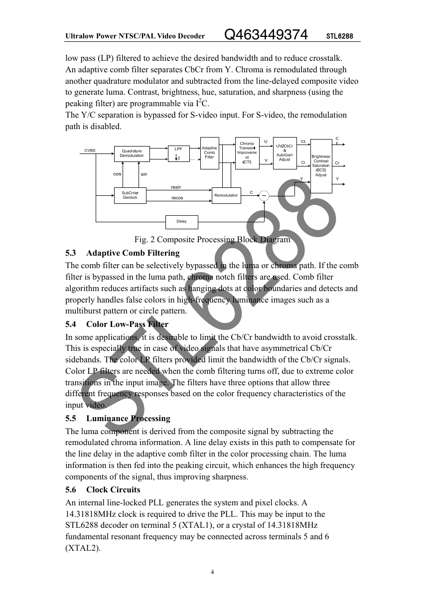
Fig.2 shows the basic architecture of this processing block.
Fig.2 shows the luminance/chrominance (Y/C) separation process in the STL6288
decoder. The composite video is multiplied by subcarrier signals in the quadrature
modulator to generate the color difference signals Cb and Cr. Cb and Cr are then
3
�
Ultralow Power NTSC/PAL Video Decoder STL6288
Q463449374
low pass (LP) filtered to achieve the desired bandwidth and to reduce crosstalk.
An adaptive comb filter separates CbCr from Y. Chroma is remodulated through
another quadrature modulator and subtracted from the line-delayed composite video
to generate luma. Contrast, brightness, hue, saturation, and sharpness (using the
peaking filter) are programmable via I2C.
The Y/C separation is bypassed for S-video input. For S-video, the remodulation
path is disabled.
Fig. 2 Composite Processing Block Diagram
5.3 Adaptive Comb Filtering
The comb filter can be selectively bypassed in the luma or chroma path. If the comb
filter is bypassed in the luma path, chroma notch filters are used. Comb filter
algorithm reduces artifacts such as hanging dots at color boundaries and detects and
properly handles false colors in high-frequency luminance images such as a
multiburst pattern or circle pattern.
5.4 Color Low-Pass Filter
In some applications, it is desirable to limit the Cb/Cr bandwidth to avoid crosstalk.
This is especially true in case of video signals that have asymmetrical Cb/Cr
sidebands. The color LP filters provided limit the bandwidth of the Cb/Cr signals.
Color LP filters are needed when the comb filtering turns off, due to extreme color
transitions in the input image. The filters have three options that allow three
different frequency responses based on the color frequency characteristics of the
input video.
5.5 Luminance Processing
The luma component is derived from the composite signal by subtracting the
remodulated chroma information. A line delay exists in this path to compensate for
the line delay in the adaptive comb filter in the color processing chain. The luma
information is then fed into the peaking circuit, which enhances the high frequency
components of the signal, thus improving sharpness.
5.6 Clock Circuits
An internal line-locked PLL generates the system and pixel clocks. A
14.31818MHz clock is required to drive the PLL. This may be input to the
STL6288 decoder on terminal 5 (XTAL1), or a crystal of 14.31818MHz
fundamental resonant frequency may be connected across terminals 5 and 6
(XTAL2).
4
�
Ultralow Power NTSC/PAL Video Decoder STL6288
Q463449374
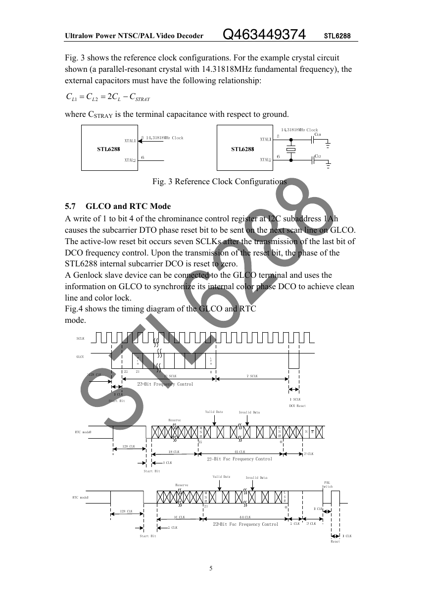
Fig. 3 shows the reference clock configurations. For the example crystal circuit
shown (a parallel-resonant crystal with 14.31818MHz fundamental frequency), the
external capacitors must have the following relationship:
C
C
2
C
=
=
−
C
L
STRAY
L
1
L
2
where CSTRAY is the terminal capacitance with respect to ground.
Fig. 3 Reference Clock Configurations
5.7 GLCO and RTC Mode
A write of 1 to bit 4 of the chrominance control register at I2C subaddress 1Ah
causes the subcarrier DTO phase reset bit to be sent on the next scan line on GLCO.
The active-low reset bit occurs seven SCLKs after the transmission of the last bit of
DCO frequency control. Upon the transmission of the reset bit, the phase of the
STL6288 internal subcarrier DCO is reset to zero.
A Genlock slave device can be connected to the GLCO terminal and uses the
information on GLCO to synchronize its internal color phase DCO to achieve clean
line and color lock.
Fig.4 shows the timing diagram of the GLCO and RTC
mode.
5
�
Ultralow Power NTSC/PAL Video Decoder STL6288
Q463449374
Fig. 4 GLCO and RTC Timing
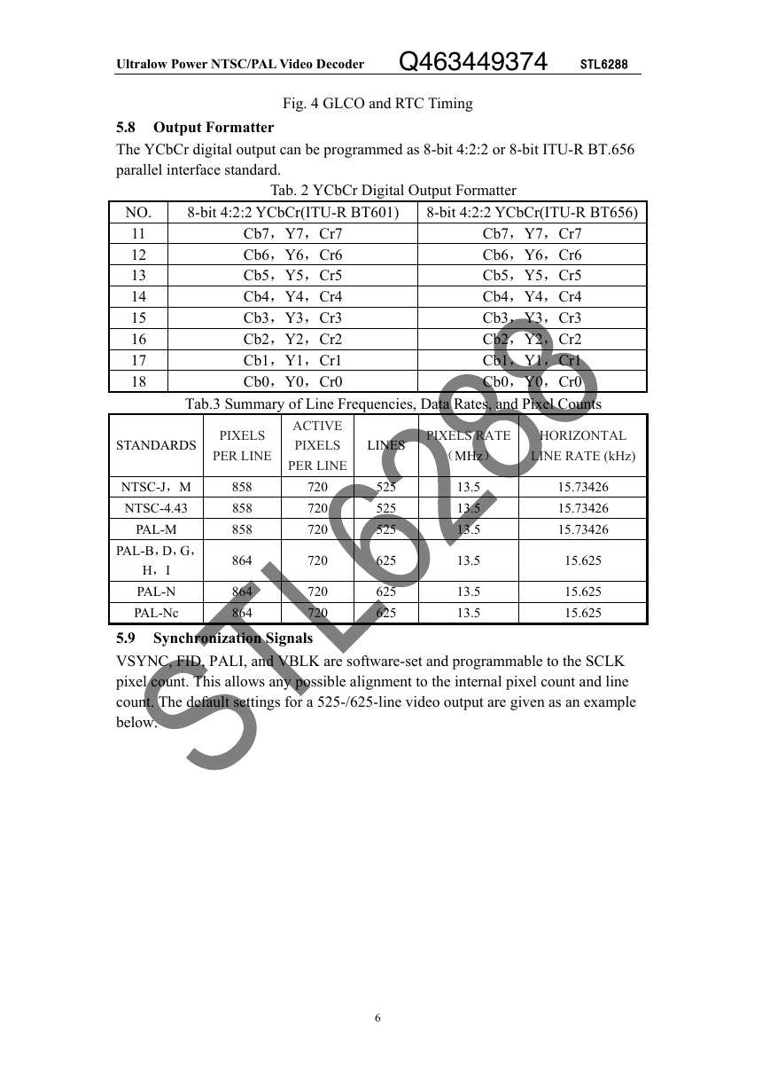
5.8 Output Formatter
The YCbCr digital output can be programmed as 8-bit 4:2:2 or 8-bit ITU-R BT.656
parallel interface standard.
Tab. 2 YCbCr Digital Output Formatter
NO.
11
12
13
14
15
16
17
18
8-bit 4:2:2 YCbCr(ITU-R BT601)
8-bit 4:2:2 YCbCr(ITU-R BT656)
Cb7,Y7,Cr7
Cb6,Y6,Cr6
Cb5,Y5,Cr5
Cb4,Y4,Cr4
Cb3,Y3,Cr3
Cb2,Y2,Cr2
Cb1,Y1,Cr1
Cb0,Y0,Cr0
Cb7,Y7,Cr7
Cb6,Y6,Cr6
Cb5,Y5,Cr5
Cb4,Y4,Cr4
Cb3,Y3,Cr3
Cb2,Y2,Cr2
Cb1,Y1,Cr1
Cb0,Y0,Cr0
Tab.3 Summary of Line Frequencies, Data Rates, and Pixel Counts
STANDARDS
NTSC-J,M
NTSC-4.43
PAL-M
PAL-B,D,G,
H,I
PAL-N
PAL-Nc
PIXELS
PER LINE
ACTIVE
PIXELS
PER LINE
LINES
PIXELS RATE
(MHz)
HORIZONTAL
LINE RATE (kHz)
858
858
858
864
864
864
720
720
720
720
720
720
525
525
525
625
625
625
13.5
13.5
13.5
13.5
13.5
13.5
15.73426
15.73426
15.73426
15.625
15.625
15.625
5.9 Synchronization Signals
VSYNC, FID, PALI, and VBLK are software-set and programmable to the SCLK
pixel count. This allows any possible alignment to the internal pixel count and line
count. The default settings for a 525-/625-line video output are given as an example
below.
6
�




 2023年江西萍乡中考道德与法治真题及答案.doc
 2012年重庆南川中考生物真题及答案.doc
 2013年江西师范大学地理学综合及文艺理论基础考研真题.doc
 2020年四川甘孜小升初语文真题及答案I卷.doc
 2020年注册岩土工程师专业基础考试真题及答案.doc
 2023-2024学年福建省厦门市九年级上学期数学月考试题及答案.doc
 2021-2022学年辽宁省沈阳市大东区九年级上学期语文期末试题及答案.doc
 2022-2023学年北京东城区初三第一学期物理期末试卷及答案.doc
 2018上半年江西教师资格初中地理学科知识与教学能力真题及答案.doc
 2012年河北国家公务员申论考试真题及答案-省级.doc
 2020-2021学年江苏省扬州市江都区邵樊片九年级上学期数学第一次质量检测试题及答案.doc
 2022下半年黑龙江教师资格证中学综合素质真题及答案.doc