TI Designs
Industrial Battery Management Module for 20S
applications Reference Design
Design Overview
Design Features
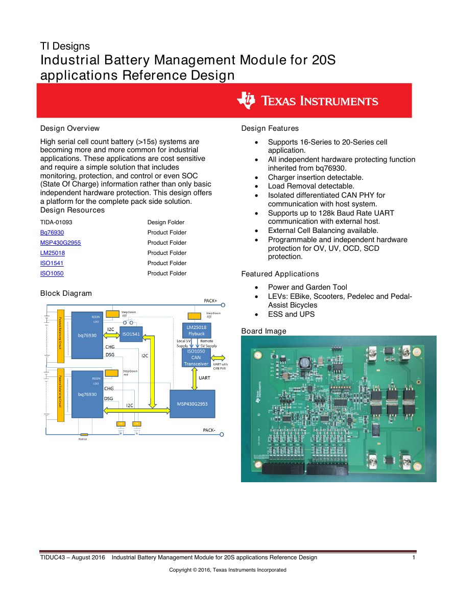
High serial cell count battery (>15s) systems are
becoming more and more common for industrial
applications. These applications are cost sensitive
and require a simple solution that includes
monitoring, protection, and control or even SOC
(State Of Charge) information rather than only basic
independent hardware protection. This design offers
a platform for the complete pack side solution.
Design Resources
TIDA-01093
Bq76930
MSP430G2955
LM25018
ISO1541
ISO1050
Block Diagram
Design Folder
Product Folder
Product Folder
Product Folder
Product Folder
Product Folder
Supports 16-Series to 20-Series cell
application.
All independent hardware protecting function
inherited from bq76930.
Charger insertion detectable.
Load Removal detectable.
Isolated differentiated CAN PHY for
communication with host system.
Supports up to 128k Baud Rate UART
communication with external host.
External Cell Balancing available.
Programmable and independent hardware
protection for OV, UV, OCD, SCD
protection.
Featured Applications
Power and Garden Tool
LEVs: EBike, Scooters, Pedelec and Pedal-
Assist Bicycles
ESS and UPS
Board Image
TIDUC43 – August 2016
Industrial Battery Management Module for 20S applications Reference Design
1
Copyright © 2016, Texas Instruments Incorporated
�
www.ti.com
1 Key System Specifications
PARAMETER
Cell Series Number
Max Stack Voltage
Consumption
Current
Balancing Current
Additional FETs
Shutdown Delay
caused by the OR
circuits in block
diagram
Support Baud Rate
Minimum Gap
Between PACK- and
BAT- for Charger
Detection
Load Detect removal
Delay
Table 1: Key System Specifications
SPEDIFICATION
Details
Shutdown
Normal(MCU in LPM3,
bq76930 ADC On, bq76930
CC Off)
Normal(MCU On, bq76930
ADC On, bq76930 CC On)
Communication with host
Discharge
Charge
16s to 20s
144V
0.6uA typical
60uA typical
4.5mA typical
17.5mA typical
40mA typical
48.6uS typical
372.4uS typical
38.4kBit/S ~ 128kBit/S
2V
~408.1s
Stack Voltage =
80v
TIDUC43 - August 2016
Industrial Battery Management Module for 20S applications Reference Design
2
Copyright © 2016, Texas Instruments Incorporated
�
www.ti.com
2 System Description
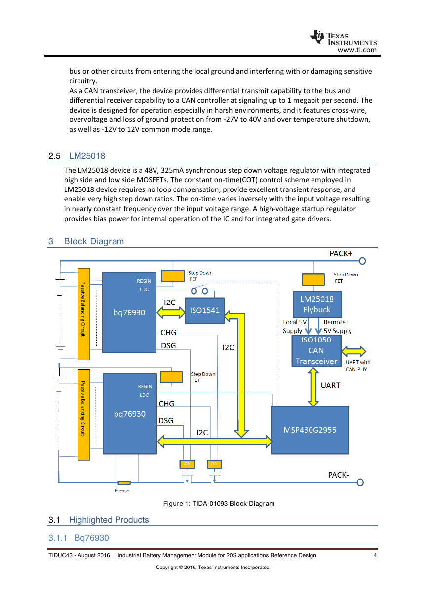
This design incorporates two bq76930 devices and one MCU MSP430G2955 to monitor 16 to 20
cells connected in series, with the typical overall battery stack voltage ranges from 50v(2.5v for
each cell) to 84v(4.2v for each cell). The MCU communicates with each bq76930 with
multiplexed I2C buses alternately. An I2C isolator ISO1541 is used for the MCU to access the
upper bq76930. The MCU can also act as a slave device to respond the access from external host
with isolated differentiated CAN PHY, facilitated with ISO1050 and its internal UART module. A
FLYBUCK DCDC controller is used to provide 2 isolated power rails to ISO1050. The FETs control
signals from each bq76930 are synthesized with the OR circuits in Figure 1 to control charge and
discharge FETs respectively. All independent hardware controlled protect functions are inherited
from bq76930.
2.1 Bq76930
The bq76930 device supports 6-series to 10-series cell battery pack, a variety of battery
chemistries including Lithium ion, Lithium Iron Phosphate and more may be managed by this
device. Via I2C, a host controller can use the bq769x0 to implement many battery pack
management functions, such as monitoring (cell voltages, pack current, pack temperatures),
protection (controlling charge/discharge FETs), and balancing. Integrated A/D converters
enable a purely digital readout of critical system parameters, with calibration handled in TI’s
manufacturing process.
2.2 MSP430G2955
The MSP430G2955 series is an ultra-low-power mixed signal microcontrollers with built-in 16-bit
timers, up to 32 I/O touch-sense-enabled pins, a versatile analog comparator, and built-in
communication capability using the universal serial communication interface. For detail
configurations, please refer to table 2
Table 2: MSP430G2955 Configurations
Device
BSL
EEM
Flash
(KB)
RAM
(B)
Timer_A
Timer_B
COMP_A+
Channels
ADC10
Channels
USCI_A0
USCI_B0
Clock
I/O
Package
Type
MSP430G2955IDA38
1
1
56
4096
2xTA3
1xTB3
8
12
1
HF, LF,
DCO, VLO
32
38-TSSOP
2.3
ISO1541
ISO1451 device is a lower power, bidirectional isolators that are compatible with I2C interfaces,
the device has its logic input and output buffers separated by TI’s Capacitive Isolation
technology using a silicon dioxide barrier. When used with isolated power supplies, this device
blocks high voltages, isolates grounds, and prevents noise currents from entering the local
ground and interfering with or damaging sensitive circuitry. The ISO1541 has a bidirectional
data and a unidirectional clock channel which is suitable for a single master system.
2.4
ISO1050
The ISO1050 is a galvanically isolated CAN transceiver that meets the specification of the
ISO11898-2 standard. The device has the input and output logical buffers separated by silicon
oxide insulation barrier that provides galvanic isolation of up to 2500VRMS for ISO1050DUB.
Used in conjunction with isolated power supplies, the device prevents noise current on a data
TIDUC43 - August 2016
Industrial Battery Management Module for 20S applications Reference Design
3
Copyright © 2016, Texas Instruments Incorporated
�
www.ti.com
bus or other circuits from entering the local ground and interfering with or damaging sensitive
circuitry.
As a CAN transceiver, the device provides differential transmit capability to the bus and
differential receiver capability to a CAN controller at signaling up to 1 megabit per second. The
device is designed for operation especially in harsh environments, and it features cross-wire,
overvoltage and loss of ground protection from -27V to 40V and over temperature shutdown,
as well as -12V to 12V common mode range.
2.5 LM25018
The LM25018 device is a 48V, 325mA synchronous step down voltage regulator with integrated
high side and low side MOSFETs. The constant on-time(COT) control scheme employed in
LM25018 device requires no loop compensation, provide excellent transient response, and
enable very high step down ratios. The on-time varies inversely with the input voltage resulting
in nearly constant frequency over the input voltage range. A high-voltage startup regulator
provides bias power for internal operation of the IC and for integrated gate drivers.
3 Block Diagram
Figure 1: TIDA-01093 Block Diagram
3.1 Highlighted Products
3.1.1 Bq76930
TIDUC43 - August 2016
Industrial Battery Management Module for 20S applications Reference Design
Copyright © 2016, Texas Instruments Incorporated
4
�
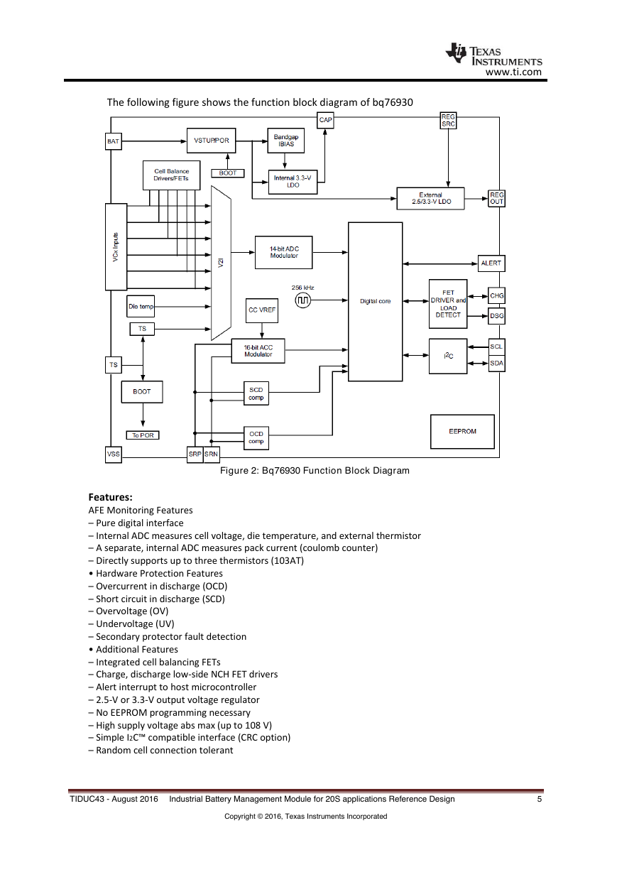
The following figure shows the function block diagram of bq76930
www.ti.com
Figure 2: Bq76930 Function Block Diagram
Features:
AFE Monitoring Features
– Pure digital interface
– Internal ADC measures cell voltage, die temperature, and external thermistor
– A separate, internal ADC measures pack current (coulomb counter)
– Directly supports up to three thermistors (103AT)
• Hardware Protection Features
– Overcurrent in discharge (OCD)
– Short circuit in discharge (SCD)
– Overvoltage (OV)
– Undervoltage (UV)
– Secondary protector fault detection
• Additional Features
– Integrated cell balancing FETs
– Charge, discharge low-side NCH FET drivers
– Alert interrupt to host microcontroller
– 2.5-V or 3.3-V output voltage regulator
– No EEPROM programming necessary
– High supply voltage abs max (up to 108 V)
– Simple I2C™ compatible interface (CRC option)
– Random cell connection tolerant
TIDUC43 - August 2016
Industrial Battery Management Module for 20S applications Reference Design
5
Copyright © 2016, Texas Instruments Incorporated
�
www.ti.com
4 System Design Theory
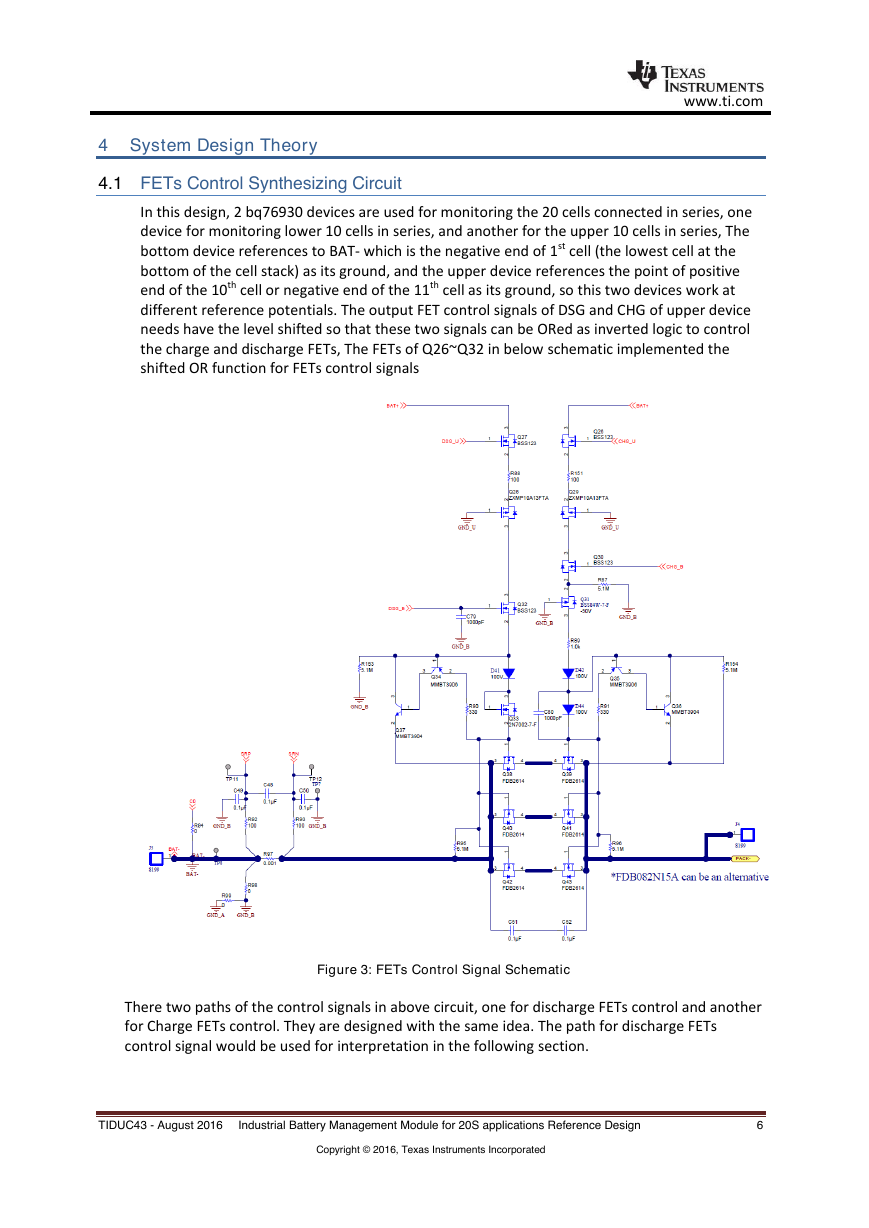
4.1 FETs Control Synthesizing Circuit
In this design, 2 bq76930 devices are used for monitoring the 20 cells connected in series, one
device for monitoring lower 10 cells in series, and another for the upper 10 cells in series, The
bottom device references to BAT- which is the negative end of 1st cell (the lowest cell at the
bottom of the cell stack) as its ground, and the upper device references the point of positive
end of the 10th cell or negative end of the 11th cell as its ground, so this two devices work at
different reference potentials. The output FET control signals of DSG and CHG of upper device
needs have the level shifted so that these two signals can be ORed as inverted logic to control
the charge and discharge FETs, The FETs of Q26~Q32 in below schematic implemented the
shifted OR function for FETs control signals
Figure 3: FETs Control Signal Schematic
There two paths of the control signals in above circuit, one for discharge FETs control and another
for Charge FETs control. They are designed with the same idea. The path for discharge FETs
control signal would be used for interpretation in the following section.
TIDUC43 - August 2016
Industrial Battery Management Module for 20S applications Reference Design
6
Copyright © 2016, Texas Instruments Incorporated
�
www.ti.com
Given that the voltage at BAT+ in Figure 3 is 80V, and both DSG outputs of upper and bottom
devices assert upon initializing with no fault detected. With the DSG output of upper device
labeled as DSG_U asserts, the voltage of DSG_U to the ground reference GND_U for upper device
would be ~12v, since the ground reference of upper device is in the middle of battery stack, the
voltage between GND_U and GND_B is ~40V, as the GND_B is the ground reference of the
bottom device. Then the voltage of DSG_U to the GND_B is ~52V, with the typical Vgs(th) of Q27
being about 1.7V, the voltage at the source of Q27 is about 52V – 1.7V = 50.3V. With this voltage
at the source of FET Q28, this FET is on, and the voltage at Q32 drain is also 50.3V. With DSG_B
asserts at ~12V to GND_B, the voltage at source of Q32 is also clamped at ~10.3v, subtracting the
forward voltage of D41 and Vgs of Q33 summed at 2.6V, the voltage at the gates of Q38, Q40,
Q42 is about 7.7v, thus the DSG FETs are all turned on.
If the DSG output of bottom device deasserts, then the DSG_B would be ~0V, the source of Q32
would be 0V, this turns off all discharge FETs.
If the DSG output of upper device deasserts, then FETs Q27 and Q28 are turned off, the voltage at
the drain of Q28 drops to 0, this also turns off all discharge FETs.
One thing should be noted is that when the voltage at Q32 source starts to drop either caused by
deassertion of upper or bottom devices’ DSG outputs, it drops slowly if there is no additional
pulldown circuit. Q34, Q37, D41, D43 constitute an expedite shutdown circuit so that the voltage
at the gates of the discharges FETs drops quickly.
4.2 Charger Detection Circuit
Like most of the battery packs, the charger connection to the charge input end between PACK+
and PACK- in this design should be sensed by the system either when the charge FETs are open
or closed. The purposes of this are for fault detection, fault recovery, system activation from
Shutdown mode and coulomb counting if SOC information is required. In the case when charge
FETs are closed, the charge current can be sensed by bq76930 and the MCU, if the charge
current is too low to be sensed, charger detection is typically not required in most application
scenarios. As for a 20s battery, charging is almost always terminated either by full charge
detection or OV conditions, for both of the scenario, the charge FETs cut off the charge current
before the charge current tapers to 0.
When the charge FETs are open, there should be a voltage gap between charger output and
battery stack side since the charge FETs are always cut off before the current tapers to 0. The
Charger Detection Circuit senses this voltage as the measure to detect the charger presence.
Figure 4 is the schematic of this circuit.
TIDUC43 - August 2016
Industrial Battery Management Module for 20S applications Reference Design
7
Copyright © 2016, Texas Instruments Incorporated
�
www.ti.com
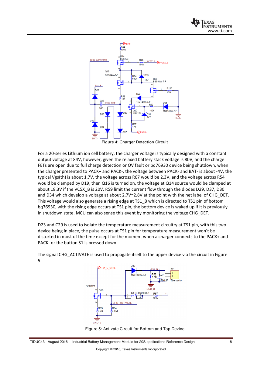
Figure 4: Charger Detection Circuit
For a 20-series Lithium ion cell battery, the charger voltage is typically designed with a constant
output voltage at 84V, however, given the relaxed battery stack voltage is 80V, and the charge
FETs are open due to full charge detection or OV fault or bq76930 device being shutdown, when
the charger presented to PACK+ and PACK-, the voltage between PACK- and BAT- is about -4V, the
typical Vgs(th) is about 1.7V, the voltage across R67 would be 2.3V, and the voltage across R54
would be clamped by D19, then Q16 is turned on, the voltage at Q14 source would be clamped at
about 18.3V if the VC5X_B is 20V. R59 limit the current flow through the diodes D29, D37, D30
and D34 which develop a voltage at about 2.7V~2.8V at the point with the net label of CHG_DET.
This voltage would also generate a rising edge at TS1_B which is directed to TS1 pin of bottom
bq76930, with the rising edge occurs at TS1 pin, the bottom device is waked up if it is previously
in shutdown state. MCU can also sense this event by monitoring the voltage CHG_DET.
D23 and C29 is used to isolate the temperature measurement circuitry at TS1 pin, with this two
device being in place, the pulse occurs at TS1 pin for temperature measurement won’t be
distorted in most of the time except for the moment when a charger connects to the PACK+ and
PACK- or the button S1 is pressed down.
The signal CHG_ACTIVATE is used to propagate itself to the upper device via the circuit in Figure
5.
Figure 5: Activate Circuit for Bottom and Top Device
TIDUC43 - August 2016
Industrial Battery Management Module for 20S applications Reference Design
8
Copyright © 2016, Texas Instruments Incorporated
�



 2023年江西萍乡中考道德与法治真题及答案.doc
 2012年重庆南川中考生物真题及答案.doc
 2013年江西师范大学地理学综合及文艺理论基础考研真题.doc
 2020年四川甘孜小升初语文真题及答案I卷.doc
 2020年注册岩土工程师专业基础考试真题及答案.doc
 2023-2024学年福建省厦门市九年级上学期数学月考试题及答案.doc
 2021-2022学年辽宁省沈阳市大东区九年级上学期语文期末试题及答案.doc
 2022-2023学年北京东城区初三第一学期物理期末试卷及答案.doc
 2018上半年江西教师资格初中地理学科知识与教学能力真题及答案.doc
 2012年河北国家公务员申论考试真题及答案-省级.doc
 2020-2021学年江苏省扬州市江都区邵樊片九年级上学期数学第一次质量检测试题及答案.doc
 2022下半年黑龙江教师资格证中学综合素质真题及答案.doc