logo资料库

PCIE4.0_CEM_SPEC.pdf

第1页 / 共193页
第2页 / 共193页
第3页 / 共193页
第4页 / 共193页
第5页 / 共193页
第6页 / 共193页
第7页 / 共193页
第8页 / 共193页
资料共193页,剩余部分请下载后查看
November 27, 2018
1. Introduction
1.1. Terms and Definitions
1.2. Reference Documents
1.3. Specification Contents
1.4. Objectives
1.5. Electrical Overview
1.6. Mechanical Overview
1.7. 150 W Overview
1.8. 225 W and 300 W Add-in Card Overview
2. Auxiliary Signals
2.1. Reference Clock
2.1.1. Low Voltage Swing, Differential Clocks
2.1.2. Spread Spectrum Clocking (SSC)
2.1.3. REFCLK AC Specifications
2.1.4. REFCLK Phase Jitter Specification for 2.5 GT/s, 5.0 GT/s, 8.0 GT/s and 16.0GT/s Signaling Support
2.2. PERST# Signal
2.2.1. Initial Power Up (G3 to S0)
2.2.2. Power Management States (S0 to S3/S4 to S0)
2.2.3. Power Down
2.3. WAKE# Signal
2.4. SMBus (Optional)
2.4.1. Capacitive Load of High-power SMBus Lines
2.4.2. Minimum Current Sinking Requirements for SMBus Devices
2.4.3. SMBus “Back Powering” Considerations
2.4.4. Power-on Reset
2.5. JTAG Pins (Optional)
2.6. PWRBRK# Signal (Optional)
2.7. Auxiliary Signal Parametric Specifications
2.7.1. DC Specifications
2.7.2. AC Specifications
3. Hot insertion and Hot removal
3.1. Scope
3.2. Presence Detect
4. Electrical Requirements
4.1. Power Supply Requirements
4.2. Power Consumption
4.3. Power Budgeting Capability
4.4. Power Supply Sequencing
4.5. Power Supply Decoupling
4.6. Electrical Topologies and Link Definitions
4.6.1. Topologies
4.6.2. Link Definition
4.7. Electrical Budgets
4.7.1. AC Coupling Capacitors
4.7.2. Insertion Loss Values (Voltage Transfer Function)
4.7.3. Jitter Values
4.7.4. Crosstalk
4.7.5. Lane-to-Lane Skew
4.7.6. Transmitter Equalization
4.7.7. Skew within the Differential Pair
4.7.8. Differential Data Trace Impedance
4.7.9. Differential Data Trace Propagation Delay
4.7.10. Add-in Card Insertion Loss Limit for 16.0 GT/s
4.8. Eye Diagrams at the Add-in Card Interface
4.8.1. Add-in Card Transmitter Path Compliance Eye Diagram at 2.5 GT/s
4.8.2. Add-in Card Transmitter Path Compliance Eye Diagrams at 5.0 GT/s
4.8.3. Add-in Card Transmitter Path Compliance Eye Diagrams at 8.0 GT/s
4.8.4. Add-in Card Transmitter Path Compliance Eye Diagrams at 16.0 GT/s
4.8.5. Add-in Card Transmitter Path Pulse Width Jitter at 16.0 GT/s
4.8.6. Add-in Card Minimum Receiver Path Sensitivity Requirements at 2.5 GT/s
4.8.7. Add-in Card Minimum Receiver Path Sensitivity Requirements at 5.0 GT/s
4.8.8. Add-in Card Minimum Receiver Path Sensitivity Requirements at 8.0 GT/s
4.8.9. Add-in Card Minimum Receiver Path Sensitivity Requirements at 16.0 GT/s
4.8.10. System Board Transmitter Path Compliance Eye Diagram at 2.5 GT/s
4.8.11. System Board Transmitter Path Compliance Eye Diagram at 5.0 GT/s
4.8.12. System Board Transmitter Path Compliance Eye Diagram at 8.0 GT/s
4.8.13. System Board Transmitter Path Compliance Eye Diagram at 16.0 GT/s
4.8.14. System Board Minimum Receiver Path Sensitivity Requirements at 2.5 GT/s
4.8.15. System Board Minimum Receiver Path Sensitivity Requirements at 5.0 GT/s
4.8.16. System Board Minimum Receiver Path Sensitivity Requirements at 8.0 GT/s
4.8.17. System Board Minimum Receiver Path Sensitivity Requirements at 16.0 GT/s
5. 150 W, 225 W, and 300 W Add-in Card Power
5.1. 150 W Add-in Card Power-Up Sequencing
5.2. 225 W and 300 W Add-in Card Power-Up Sequencing
6. Card Connector Specification
6.1. Connector Pinout
6.2. Connector Interface Definitions
6.3. Signal Integrity Requirements and Test Procedures
6.3.1. Signal Integrity Requirements
6.3.2. Signal Integrity Requirements and Test Procedures for 2.5 GT/s Support
6.3.3. Signal Integrity Requirements and Test Procedures for 5.0 GT/s Support
6.3.3.1 Test Fixture Requirements
6.3.4. Signal Integrity Requirements and Test Procedures for 8.0 GT/s Support
6.3.4.1 Test Fixture Requirements
6.3.5. Signal Integrity Requirements and Test Procedures for 16.0 GT/s Support
6.3.5.1 Test Fixture Requirements
6.4. Connector Environmental and Other Requirements
6.4.1. Environmental Requirements
6.4.2. Mechanical Requirements
6.4.3. Current Rating Requirement
6.4.4. Additional Considerations
7. PCI Express 2 x 3 Auxiliary Power Connector Definition
7.1. 6-Position Power Connector System Performance Requirements
7.2. 6-Position PCB Header
7.2.1. 6-Position R/A Thru-Hole PCB Header Assembly
7.2.2. 6-Position R/A Thru-Hole Header Recommended PCB Footprint
7.2.3. 6-Position R/A SMT PCB Header Assembly
7.2.4. 6-Position R/A SMT Header Recommended PCB Footprint
7.3. 6-Position Cable Assembly
7.4. Connector Mating-Unmating Keepout Area (Latch Lock Release)
7.5. 6-Position Power Connector System Pin Assignment
7.6. Additional Considerations
8. PCI Express 2 x 4 Auxiliary Power Connector Definition
8.1. 2 x 4 Auxiliary Power Connector Performance Requirements
8.2. 2 x 4 Receptacle
8.2.1. Connector Drawing
8.2.2. PCB Footprint
8.3. Cable Assembly
8.4. Connector Mating-Unmating Keepout Area (Latch Lock Release)
8.5. 2 x 4 Auxiliary Power Connector System Pin Assignment
8.6. Additional Considerations
9. Add-in Card Form Factors and Implementation
9.1. Add-in Card Form Factors
9.2. Add-in Card Layout Requirements and Recommendations for 16.0 GT/s Operation
9.2.1. Voiding and Planes Under Edge-fingers
9.2.2. No Add-in Card Depopulated or Floating Edge-fingers
9.2.3. Edge-finger Length and Outer Layer Keepout
9.2.4. Add-in Card Adjacent Edge-finger Ground Vias
9.2.5. Joined Edge-finger Ground Vias
9.2.6. Auxiliary Signal Conductor AC Match Termination
System Board Requirements for 16.0 GT/s Operation
9.3.1. Sentry Ground Vias Adjacent to Auxiliary Signal Vias
9.4. Connector and Add-in Card Locations
9.5. Card Interoperability
9.6. 10 W/25 W/75 W/150 W Thermal Characterization
9.7. 150 W Thermal Management
10. PCI Express 225 W/300 W Add-in Card Thermal and Acoustic Management
10.1. Inlet Temperature
10.2. Card Thermal Characterization Procedure
10.3. Acoustic Management
10.3.1. Background and Scope
10.3.2. Card Acoustic Characterization Procedure
10.3.3. Acoustic Recommendations and Guidelines
11. Adapter Add-in Card Thermal Reporting
11.1. Airflow Impedance (AFI) Level
11.2. Maximum Thermal (MaxTherm) Level
11.3. Degraded Thermal (DTherm) Level
11.4. MaxAmbient
INSERTION LOSS VALUES (VOLTAGE TRANSFER FUNCTION) (INFORMATIONAL ONLY)
TEST CHANNEL SCATTERING PARAMETERS
8.0 GT/s Test Channels
16.0 GT/s Test Channels
THERMAL DATA COLLECTION AND TEST PROCEDURE
ACKNOWLEDGEMENTS
PCI Express Card Electromechanical Specification Revision 4.0, Version 0.9 November 27, 2018 1 2 3 4 5 6 7 8 9 [Please note that there is a SupplementaryFigures_rev05d_Dec09.docx that is released with this Specification. The word file includes high resolution version of the figures that are either low resolution or are missing top/left parts in the pdf version]
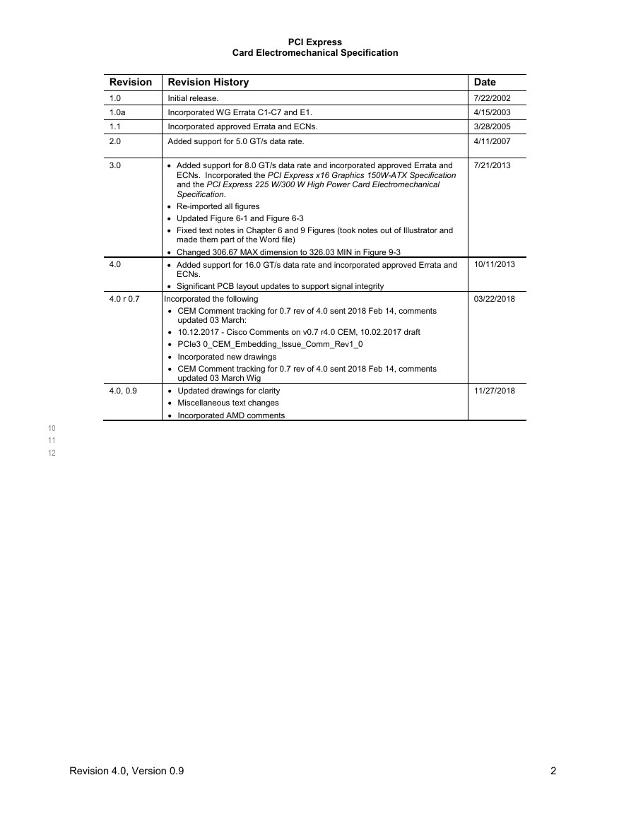
PCI Express Card Electromechanical Specification Revision Revision History 1.0 1.0a 1.1 2.0 Initial release. Incorporated WG Errata C1-C7 and E1. Incorporated approved Errata and ECNs. Added support for 5.0 GT/s data rate. 3.0 4.0 4.0 r 0.7 • Added support for 8.0 GT/s data rate and incorporated approved Errata and ECNs. Incorporated the PCI Express x16 Graphics 150W-ATX Specification and the PCI Express 225 W/300 W High Power Card Electromechanical Specification. • Re-imported all figures • Updated Figure 6-1 and Figure 6-3 • Fixed text notes in Chapter 6 and 9 Figures (took notes out of Illustrator and made them part of the Word file) • Changed 306.67 MAX dimension to 326.03 MIN in Figure 9-3 • Added support for 16.0 GT/s data rate and incorporated approved Errata and ECNs. • Significant PCB layout updates to support signal integrity Incorporated the following • CEM Comment tracking for 0.7 rev of 4.0 sent 2018 Feb 14, comments updated 03 March: • 10.12.2017 - Cisco Comments on v0.7 r4.0 CEM, 10.02.2017 draft • PCIe3 0_CEM_Embedding_Issue_Comm_Rev1_0 • Incorporated new drawings • CEM Comment tracking for 0.7 rev of 4.0 sent 2018 Feb 14, comments updated 03 March Wig 4.0, 0.9 • Updated drawings for clarity • Miscellaneous text changes • Incorporated AMD comments Date 7/22/2002 4/15/2003 3/28/2005 4/11/2007 7/21/2013 10/11/2013 03/22/2018 11/27/2018 10 11 12 Revision 4.0, Version 0.9 2
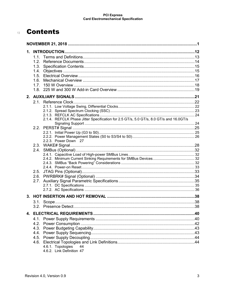
PCI Express Card Electromechanical Specification 13 Contents NOVEMBER 21, 2018 ................................................................................................................ 1 INTRODUCTION ................................................................................................................. 12 1. 1.1. Terms and Definitions ................................................................................................. 13 1.2. Reference Documents ................................................................................................ 14 1.3. Specification Contents ................................................................................................ 15 1.4. Objectives .................................................................................................................. 15 1.5. Electrical Overview ..................................................................................................... 16 1.6. Mechanical Overview ................................................................................................. 17 1.7. 150 W Overview ......................................................................................................... 18 1.8. 225 W and 300 W Add-in Card Overview ................................................................... 19 2. AUXILIARY SIGNALS ........................................................................................................ 21 2.1. Reference Clock ......................................................................................................... 22 2.1.1. Low Voltage Swing, Differential Clocks ........................................................................... 22 2.1.2. Spread Spectrum Clocking (SSC) ................................................................................... 23 2.1.3. REFCLK AC Specifications ............................................................................................. 24 2.1.4. REFCLK Phase Jitter Specification for 2.5 GT/s, 5.0 GT/s, 8.0 GT/s and 16.0GT/s Signaling Support ............................................................................................................ 24 2.2. PERST# Signal .......................................................................................................... 25 2.2.1. Initial Power Up (G3 to S0) .............................................................................................. 25 2.2.2. Power Management States (S0 to S3/S4 to S0) ............................................................. 26 2.2.3. Power Down 27 2.3. WAKE# Signal ............................................................................................................ 28 2.4. SMBus (Optional) ....................................................................................................... 32 2.4.1. Capacitive Load of High-power SMBus Lines ................................................................. 32 2.4.2. Minimum Current Sinking Requirements for SMBus Devices ......................................... 32 2.4.3. SMBus “Back Powering” Considerations ........................................................................ 32 2.4.4. Power-on Reset ............................................................................................................... 33 2.5. JTAG Pins (Optional) .................................................................................................. 33 2.6. PWRBRK# Signal (Optional) ...................................................................................... 34 2.7. Auxiliary Signal Parametric Specifications .................................................................. 35 2.7.1. DC Specifications ............................................................................................................ 35 2.7.2. AC Specifications ............................................................................................................ 36 3. HOT INSERTION AND HOT REMOVAL ............................................................................ 38 3.1. Scope ......................................................................................................................... 38 3.2. Presence Detect ......................................................................................................... 38 4. ELECTRICAL REQUIREMENTS ........................................................................................ 40 4.1. Power Supply Requirements ...................................................................................... 40 4.2. Power Consumption ................................................................................................... 42 4.3. Power Budgeting Capability ........................................................................................ 43 4.4. Power Supply Sequencing .......................................................................................... 43 4.5. Power Supply Decoupling........................................................................................... 44 4.6. Electrical Topologies and Link Definitions ................................................................... 44 4.6.1. Topologies 44 4.6.2. Link Definition 47 Revision 4.0, Version 0.9 3
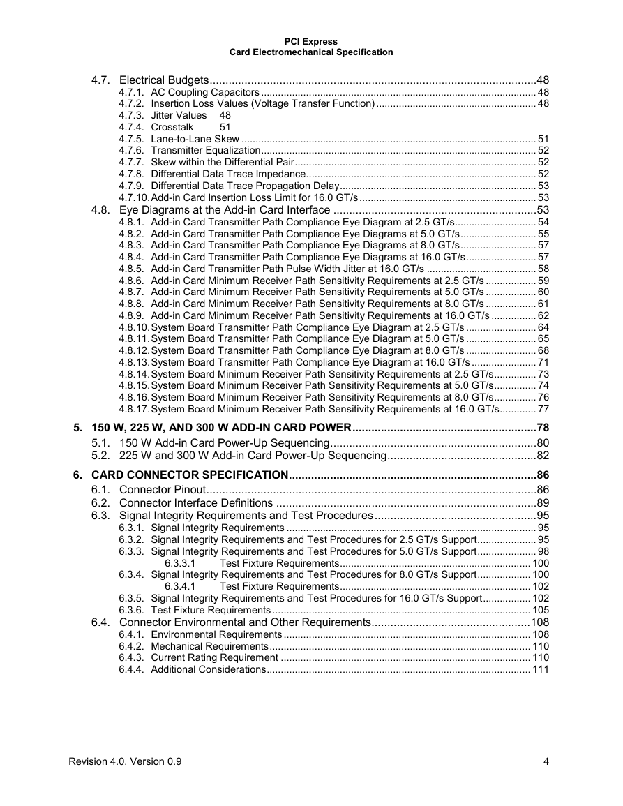
PCI Express Card Electromechanical Specification 4.7. Electrical Budgets ....................................................................................................... 48 4.7.1. AC Coupling Capacitors .................................................................................................. 48 4.7.2. Insertion Loss Values (Voltage Transfer Function) ......................................................... 48 4.7.3. Jitter Values 48 4.7.4. Crosstalk 51 4.7.5. Lane-to-Lane Skew ......................................................................................................... 51 4.7.6. Transmitter Equalization .................................................................................................. 52 4.7.7. Skew within the Differential Pair ...................................................................................... 52 4.7.8. Differential Data Trace Impedance.................................................................................. 52 4.7.9. Differential Data Trace Propagation Delay ...................................................................... 53 4.7.10. Add-in Card Insertion Loss Limit for 16.0 GT/s ............................................................... 53 4.8. Eye Diagrams at the Add-in Card Interface ................................................................ 53 4.8.1. Add-in Card Transmitter Path Compliance Eye Diagram at 2.5 GT/s ............................. 54 4.8.2. Add-in Card Transmitter Path Compliance Eye Diagrams at 5.0 GT/s ........................... 55 4.8.3. Add-in Card Transmitter Path Compliance Eye Diagrams at 8.0 GT/s ........................... 57 4.8.4. Add-in Card Transmitter Path Compliance Eye Diagrams at 16.0 GT/s ......................... 57 4.8.5. Add-in Card Transmitter Path Pulse Width Jitter at 16.0 GT/s ....................................... 58 4.8.6. Add-in Card Minimum Receiver Path Sensitivity Requirements at 2.5 GT/s .................. 59 4.8.7. Add-in Card Minimum Receiver Path Sensitivity Requirements at 5.0 GT/s .................. 60 4.8.8. Add-in Card Minimum Receiver Path Sensitivity Requirements at 8.0 GT/s .................. 61 4.8.9. Add-in Card Minimum Receiver Path Sensitivity Requirements at 16.0 GT/s ................ 62 4.8.10. System Board Transmitter Path Compliance Eye Diagram at 2.5 GT/s ......................... 64 4.8.11. System Board Transmitter Path Compliance Eye Diagram at 5.0 GT/s ......................... 65 4.8.12. System Board Transmitter Path Compliance Eye Diagram at 8.0 GT/s ......................... 68 4.8.13. System Board Transmitter Path Compliance Eye Diagram at 16.0 GT/s ....................... 71 4.8.14. System Board Minimum Receiver Path Sensitivity Requirements at 2.5 GT/s ............... 73 4.8.15. System Board Minimum Receiver Path Sensitivity Requirements at 5.0 GT/s ............... 74 4.8.16. System Board Minimum Receiver Path Sensitivity Requirements at 8.0 GT/s ............... 76 4.8.17. System Board Minimum Receiver Path Sensitivity Requirements at 16.0 GT/s ............. 77 5. 150 W, 225 W, AND 300 W ADD-IN CARD POWER .......................................................... 78 5.1. 150 W Add-in Card Power-Up Sequencing ................................................................. 80 5.2. 225 W and 300 W Add-in Card Power-Up Sequencing ............................................... 82 6. CARD CONNECTOR SPECIFICATION .............................................................................. 86 6.1. Connector Pinout ........................................................................................................ 86 6.2. Connector Interface Definitions .................................................................................. 89 6.3. Signal Integrity Requirements and Test Procedures ................................................... 95 6.3.1. Signal Integrity Requirements ......................................................................................... 95 6.3.2. Signal Integrity Requirements and Test Procedures for 2.5 GT/s Support ..................... 95 6.3.3. Signal Integrity Requirements and Test Procedures for 5.0 GT/s Support ..................... 98 Test Fixture Requirements .................................................................... 100 6.3.4. Signal Integrity Requirements and Test Procedures for 8.0 GT/s Support ................... 100 Test Fixture Requirements .................................................................... 102 6.3.5. Signal Integrity Requirements and Test Procedures for 16.0 GT/s Support ................. 102 6.3.6. Test Fixture Requirements ............................................................................................ 105 6.4. Connector Environmental and Other Requirements.................................................. 108 6.4.1. Environmental Requirements ........................................................................................ 108 6.4.2. Mechanical Requirements ............................................................................................. 110 6.4.3. Current Rating Requirement ......................................................................................... 110 6.4.4. Additional Considerations .............................................................................................. 111 6.3.3.1 6.3.4.1 Revision 4.0, Version 0.9 4
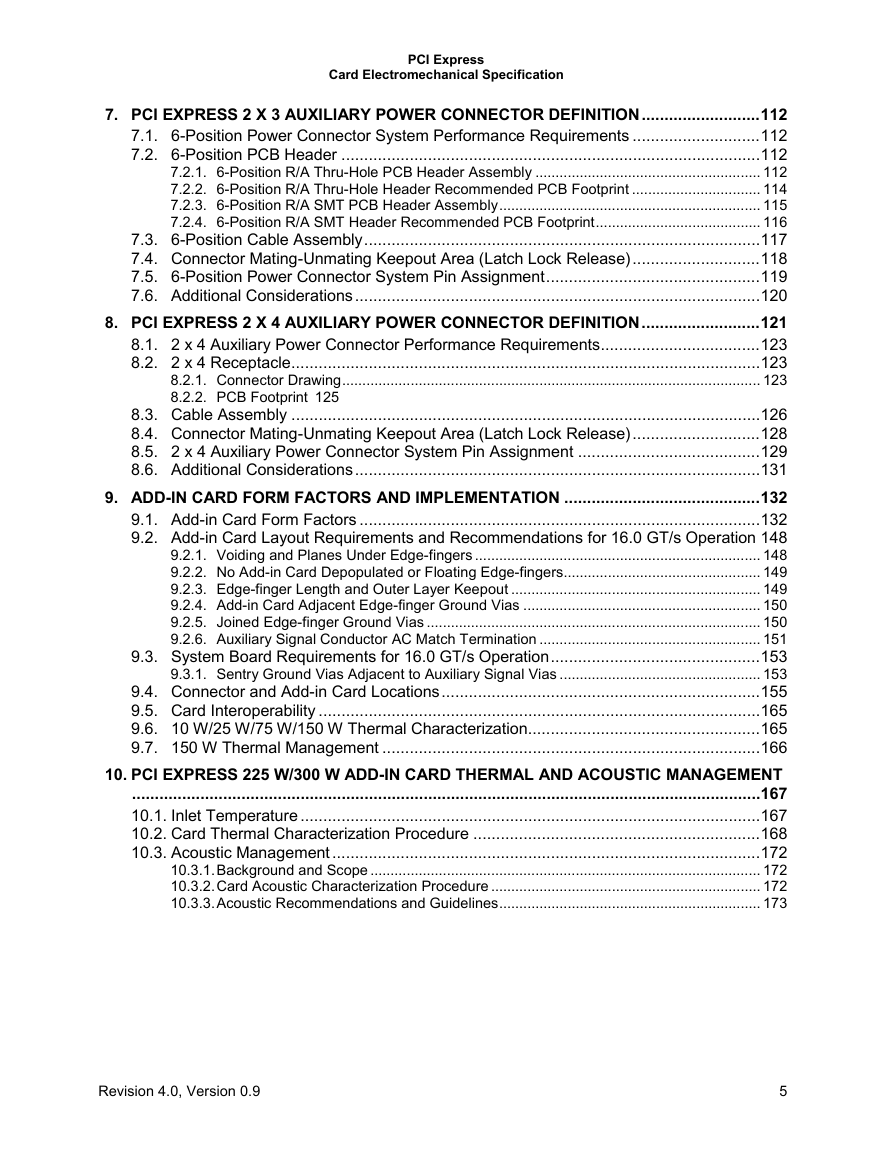
PCI Express Card Electromechanical Specification 7. PCI EXPRESS 2 X 3 AUXILIARY POWER CONNECTOR DEFINITION .......................... 112 7.1. 6-Position Power Connector System Performance Requirements ............................ 112 7.2. 6-Position PCB Header ............................................................................................ 112 7.2.1. 6-Position R/A Thru-Hole PCB Header Assembly ........................................................ 112 7.2.2. 6-Position R/A Thru-Hole Header Recommended PCB Footprint ................................ 114 7.2.3. 6-Position R/A SMT PCB Header Assembly ................................................................. 115 7.2.4. 6-Position R/A SMT Header Recommended PCB Footprint ......................................... 116 7.3. 6-Position Cable Assembly ....................................................................................... 117 7.4. Connector Mating-Unmating Keepout Area (Latch Lock Release) ............................ 118 7.5. 6-Position Power Connector System Pin Assignment ............................................... 119 7.6. Additional Considerations ......................................................................................... 120 8. PCI EXPRESS 2 X 4 AUXILIARY POWER CONNECTOR DEFINITION .......................... 121 8.1. 2 x 4 Auxiliary Power Connector Performance Requirements ................................... 123 8.2. 2 x 4 Receptacle ....................................................................................................... 123 8.2.1. Connector Drawing ........................................................................................................ 123 8.2.2. PCB Footprint 125 8.3. Cable Assembly ....................................................................................................... 126 8.4. Connector Mating-Unmating Keepout Area (Latch Lock Release) ............................ 128 8.5. 2 x 4 Auxiliary Power Connector System Pin Assignment ........................................ 129 8.6. Additional Considerations ......................................................................................... 131 9. ADD-IN CARD FORM FACTORS AND IMPLEMENTATION ........................................... 132 9.1. Add-in Card Form Factors ........................................................................................ 132 9.2. Add-in Card Layout Requirements and Recommendations for 16.0 GT/s Operation 148 9.2.1. Voiding and Planes Under Edge-fingers ....................................................................... 148 9.2.2. No Add-in Card Depopulated or Floating Edge-fingers................................................. 149 9.2.3. Edge-finger Length and Outer Layer Keepout .............................................................. 149 9.2.4. Add-in Card Adjacent Edge-finger Ground Vias ........................................................... 150 9.2.5. Joined Edge-finger Ground Vias ................................................................................... 150 9.2.6. Auxiliary Signal Conductor AC Match Termination ....................................................... 151 9.3. System Board Requirements for 16.0 GT/s Operation .............................................. 153 9.3.1. Sentry Ground Vias Adjacent to Auxiliary Signal Vias .................................................. 153 9.4. Connector and Add-in Card Locations ...................................................................... 155 9.5. Card Interoperability ................................................................................................. 165 9.6. 10 W/25 W/75 W/150 W Thermal Characterization................................................... 165 9.7. 150 W Thermal Management ................................................................................... 166 10. PCI EXPRESS 225 W/300 W ADD-IN CARD THERMAL AND ACOUSTIC MANAGEMENT .......................................................................................................................................... 167 10.1. Inlet Temperature ..................................................................................................... 167 10.2. Card Thermal Characterization Procedure ............................................................... 168 10.3. Acoustic Management .............................................................................................. 172 10.3.1. Background and Scope ................................................................................................. 172 10.3.2. Card Acoustic Characterization Procedure ................................................................... 172 10.3.3. Acoustic Recommendations and Guidelines ................................................................. 173 Revision 4.0, Version 0.9 5
PCI Express Card Electromechanical Specification 11. ADAPTER ADD-IN CARD THERMAL REPORTING ........................................................ 174 11.1. Airflow Impedance (AFI) Level .................................................................................. 174 11.2. Maximum Thermal (MaxTherm) Level ...................................................................... 176 11.3. Degraded Thermal (DTherm) Level .......................................................................... 178 11.4. MaxAmbient ............................................................................................................. 179 INSERTION LOSS VALUES (VOLTAGE TRANSFER FUNCTION) (INFORMATIONAL ONLY) ............................................................................................... 180 TEST CHANNEL SCATTERING PARAMETERS ................................................................... 183 8.0 GT/s Test Channels .................................................................................................... 183 THERMAL DATA COLLECTION AND TEST PROCEDURE ................................................. 184 ACKNOWLEDGEMENTS ....................................................................................................... 192 14 15 Revision 4.0, Version 0.9 6
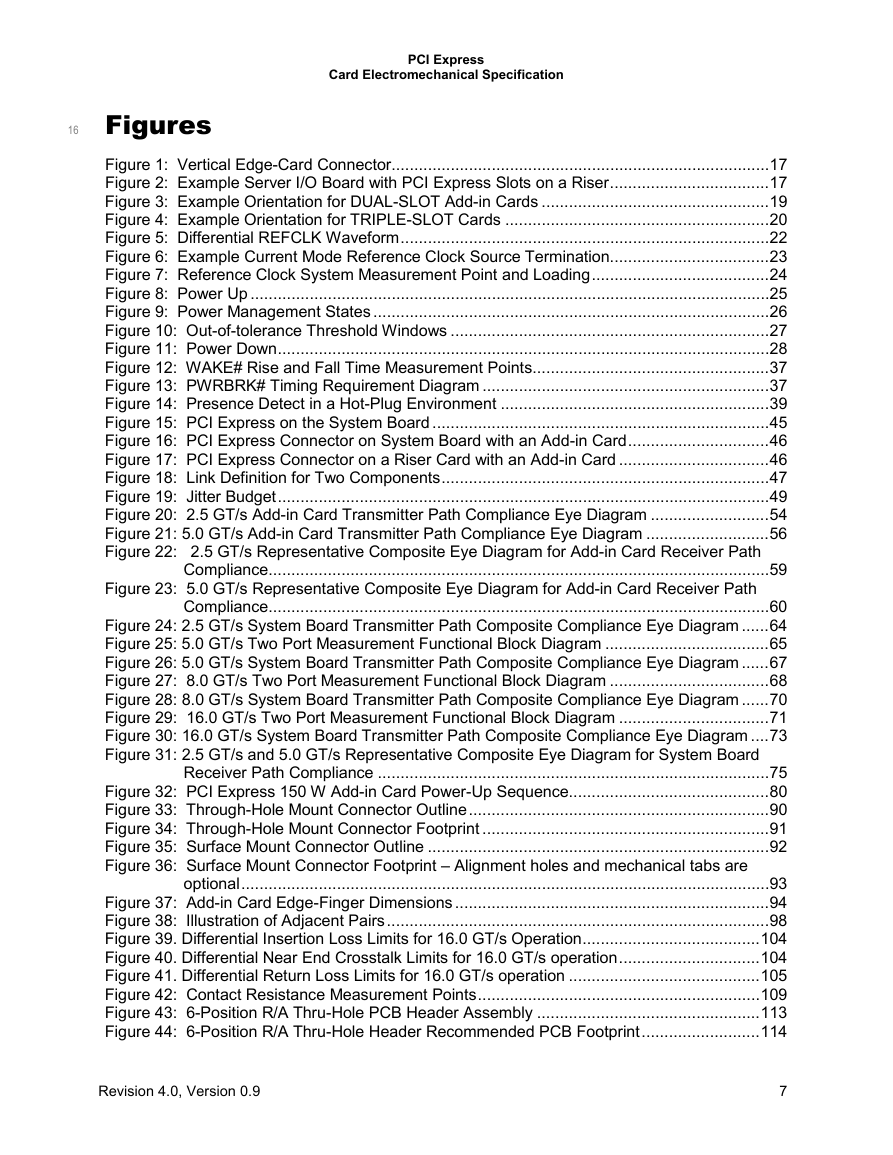
16 PCI Express Card Electromechanical Specification Figures Figure 1: Vertical Edge-Card Connector ................................................................................... 17 Figure 2: Example Server I/O Board with PCI Express Slots on a Riser ................................... 17 Figure 3: Example Orientation for DUAL-SLOT Add-in Cards .................................................. 19 Figure 4: Example Orientation for TRIPLE-SLOT Cards .......................................................... 20 Figure 5: Differential REFCLK Waveform ................................................................................. 22 Figure 6: Example Current Mode Reference Clock Source Termination................................... 23 Figure 7: Reference Clock System Measurement Point and Loading ....................................... 24 Figure 8: Power Up .................................................................................................................. 25 Figure 9: Power Management States ....................................................................................... 26 Figure 10: Out-of-tolerance Threshold Windows ...................................................................... 27 Figure 11: Power Down ............................................................................................................ 28 Figure 12: WAKE# Rise and Fall Time Measurement Points .................................................... 37 Figure 13: PWRBRK# Timing Requirement Diagram ............................................................... 37 Figure 14: Presence Detect in a Hot-Plug Environment ........................................................... 39 Figure 15: PCI Express on the System Board .......................................................................... 45 Figure 16: PCI Express Connector on System Board with an Add-in Card ............................... 46 Figure 17: PCI Express Connector on a Riser Card with an Add-in Card ................................. 46 Figure 18: Link Definition for Two Components ........................................................................ 47 Figure 19: Jitter Budget ............................................................................................................ 49 Figure 20: 2.5 GT/s Add-in Card Transmitter Path Compliance Eye Diagram .......................... 54 Figure 21: 5.0 GT/s Add-in Card Transmitter Path Compliance Eye Diagram ........................... 56 Figure 22: 2.5 GT/s Representative Composite Eye Diagram for Add-in Card Receiver Path Compliance.............................................................................................................. 59 Figure 23: 5.0 GT/s Representative Composite Eye Diagram for Add-in Card Receiver Path Compliance.............................................................................................................. 60 Figure 24: 2.5 GT/s System Board Transmitter Path Composite Compliance Eye Diagram ...... 64 Figure 25: 5.0 GT/s Two Port Measurement Functional Block Diagram .................................... 65 Figure 26: 5.0 GT/s System Board Transmitter Path Composite Compliance Eye Diagram ...... 67 Figure 27: 8.0 GT/s Two Port Measurement Functional Block Diagram ................................... 68 Figure 28: 8.0 GT/s System Board Transmitter Path Composite Compliance Eye Diagram ...... 70 Figure 29: 16.0 GT/s Two Port Measurement Functional Block Diagram ................................. 71 Figure 30: 16.0 GT/s System Board Transmitter Path Composite Compliance Eye Diagram .... 73 Figure 31: 2.5 GT/s and 5.0 GT/s Representative Composite Eye Diagram for System Board Receiver Path Compliance ...................................................................................... 75 Figure 32: PCI Express 150 W Add-in Card Power-Up Sequence............................................ 80 Figure 33: Through-Hole Mount Connector Outline .................................................................. 90 Figure 34: Through-Hole Mount Connector Footprint ............................................................... 91 Figure 35: Surface Mount Connector Outline ........................................................................... 92 Figure 36: Surface Mount Connector Footprint – Alignment holes and mechanical tabs are optional .................................................................................................................... 93 Figure 37: Add-in Card Edge-Finger Dimensions ..................................................................... 94 Figure 38: Illustration of Adjacent Pairs .................................................................................... 98 Figure 39. Differential Insertion Loss Limits for 16.0 GT/s Operation ....................................... 104 Figure 40. Differential Near End Crosstalk Limits for 16.0 GT/s operation ............................... 104 Figure 41. Differential Return Loss Limits for 16.0 GT/s operation .......................................... 105 Figure 42: Contact Resistance Measurement Points .............................................................. 109 Figure 43: 6-Position R/A Thru-Hole PCB Header Assembly ................................................. 113 Figure 44: 6-Position R/A Thru-Hole Header Recommended PCB Footprint .......................... 114 Revision 4.0, Version 0.9 7
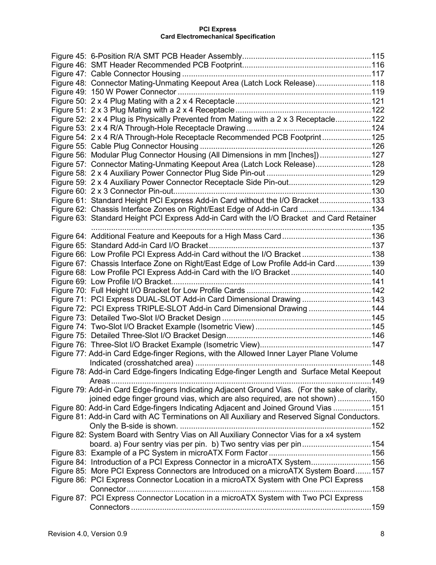
PCI Express Card Electromechanical Specification Figure 45: 6-Position R/A SMT PCB Header Assembly .......................................................... 115 Figure 46: SMT Header Recommended PCB Footprint .......................................................... 116 Figure 47: Cable Connector Housing ..................................................................................... 117 Figure 48: Connector Mating-Unmating Keepout Area (Latch Lock Release) ......................... 118 Figure 49: 150 W Power Connector ....................................................................................... 119 Figure 50: 2 x 4 Plug Mating with a 2 x 4 Receptacle ............................................................. 121 Figure 51: 2 x 3 Plug Mating with a 2 x 4 Receptacle ............................................................. 122 Figure 52: 2 x 4 Plug is Physically Prevented from Mating with a 2 x 3 Receptacle ................ 122 Figure 53: 2 x 4 R/A Through-Hole Receptacle Drawing ........................................................ 124 Figure 54: 2 x 4 R/A Through-Hole Receptacle Recommended PCB Footprint ...................... 125 Figure 55: Cable Plug Connector Housing ............................................................................. 126 Figure 56: Modular Plug Connector Housing (All Dimensions in mm [Inches]) ....................... 127 Figure 57: Connector Mating-Unmating Keepout Area (Latch Lock Release) ......................... 128 Figure 58: 2 x 4 Auxiliary Power Connector Plug Side Pin-out ............................................... 129 Figure 59: 2 x 4 Auxiliary Power Connector Receptacle Side Pin-out ..................................... 129 Figure 60: 2 x 3 Connector Pin-out ......................................................................................... 130 Figure 61: Standard Height PCI Express Add-in Card without the I/O Bracket ....................... 133 Figure 62: Chassis Interface Zones on Right/East Edge of Add-in Card ................................ 134 Figure 63: Standard Height PCI Express Add-in Card with the I/O Bracket and Card Retainer .............................................................................................................................. 135 Figure 64: Additional Feature and Keepouts for a High Mass Card ........................................ 136 Figure 65: Standard Add-in Card I/O Bracket ......................................................................... 137 Figure 66: Low Profile PCI Express Add-in Card without the I/O Bracket ............................... 138 Figure 67: Chassis Interface Zone on Right/East Edge of Low Profile Add-in Card ................ 139 Figure 68: Low Profile PCI Express Add-in Card with the I/O Bracket .................................... 140 Figure 69: Low Profile I/O Bracket.......................................................................................... 141 Figure 70: Full Height I/O Bracket for Low Profile Cards ........................................................ 142 Figure 71: PCI Express DUAL-SLOT Add-in Card Dimensional Drawing ............................... 143 Figure 72: PCI Express TRIPLE-SLOT Add-in Card Dimensional Drawing ............................ 144 Figure 73: Detailed Two-Slot I/O Bracket Design ................................................................... 145 Figure 74: Two-Slot I/O Bracket Example (Isometric View) .................................................... 145 Figure 75: Detailed Three-Slot I/O Bracket Design ................................................................. 146 Figure 76: Three-Slot I/O Bracket Example (Isometric View) .................................................. 147 Figure 77: Add-in Card Edge-finger Regions, with the Allowed Inner Layer Plane Volume Indicated (crosshatched area) ............................................................................... 148 Figure 78: Add-in Card Edge-fingers Indicating Edge-finger Length and Surface Metal Keepout Areas ..................................................................................................................... 149 Figure 79: Add-in Card Edge-fingers Indicating Adjacent Ground Vias. (For the sake of clarity, joined edge finger ground vias, which are also required, are not shown) ............... 150 Figure 80: Add-in Card Edge-fingers Indicating Adjacent and Joined Ground Vias ................. 151 Figure 81: Add-in Card with AC Terminations on All Auxiliary and Reserved Signal Conductors. Only the B-side is shown. ...................................................................................... 152 Figure 82: System Board with Sentry Vias on All Auxiliary Connector Vias for a x4 system board. a) Four sentry vias per pin. b) Two sentry vias per pin ............................... 154 Figure 83: Example of a PC System in microATX Form Factor .............................................. 156 Figure 84: Introduction of a PCI Express Connector in a microATX System ........................... 156 Figure 85: More PCI Express Connectors are Introduced on a microATX System Board ....... 157 Figure 86: PCI Express Connector Location in a microATX System with One PCI Express Connector .............................................................................................................. 158 Figure 87: PCI Express Connector Location in a microATX System with Two PCI Express Connectors ............................................................................................................ 159 Revision 4.0, Version 0.9 8
分享到:
收藏