InvenSense Inc.
Document Number: AN-XX-XXXX-XX
1745 Technology Drive, San Jose, CA, 95110 U.S.A.
Tel: +1 (408) 501-2200 Fax: +1 (408) 988-7339
Website: www.invensense.com
Revision: 1.0
Release Date: 02/21/2014
MPU Hardware Offset Registers
Application Note
A printed copy of this document is
NOT UNDER REVISION CONTROL
unless it is dated and stamped in red ink as,
“REVISION CONTROLLED COPY.”
This information furnished by InvenSense is believed to be accurate and reliable. However, no responsibility is assumed by InvenSense
for its use, or for any infringements of patents or other rights of third parties that may result from its use. Specifications are subject to
change without notice. InvenSense reserves the right to make changes to this product, including its circuits and software, in order to
improve its design and/or performance, without prior notice. InvenSense makes no warranties, neither expressed nor implied, regarding
the information and specifications contained in this document. InvenSense assumes no responsibility for any claims or damages arising
from information contained in this document, or from the use of products and services detailed therein. This includes, but is not limited
to, claims or damages based on the infringement of patents, copyrights, mask work and/or other intellectual property rights.
Certain intellectual property owned by InvenSense and described in this document is patent protected. No license is granted by
implication or otherwise under any patent or patent rights of InvenSense. This publication supersedes and replaces all information
previously supplied. Trademarks that are registered trademarks are the property of their respective companies. InvenSense sensors
should not be used or sold in the development, storage, production or utilization of any conventional or mass-destructive weapons or for
any other weapons or life threatening applications, as well as in any other life critical applications such as medical equipment,
transportation, aerospace and nuclear instruments, undersea equipment, power plant equipment, disaster prevention and crime
prevention equipment.
Copyright ©2011 InvenSense Corporation.
�
MPU Hardware Offset Registers App Note
Version #: 1.0
Release Date: 02/21/2014
TABLE OF CONTENTS
1. REVISION HISTORY ................................................................................................................................... 3
2. REFERENCE ............................................................................................................................................... 3
3. PURPOSE .................................................................................................................................................... 3
4. DATA SIGNAL DIAGRAM .......................................................................................................................... 3
5. FINDING THE OFFSET BIASES FOR ACCEL AND GYRO ...................................................................... 4
5.1
EXAMPLE CODE FROM MOTION DRIVER 5.1.2 ....................................................................................... 4
6. GYRO OFFSET REGISTERS ...................................................................................................................... 5
6.1
6.2
6.3
REGISTER LOCATION ........................................................................................................................... 5
REGISTER FORMAT AND DESCRIPTIONS ................................................................................................ 5
EXAMPLE CODE FROM MOTION DRIVER 5.1.2 ....................................................................................... 6
7. ACCEL OFFSET REGISTERS .................................................................................................................... 6
7.1
7.2
7.3
REGISTER LOCATIONS ......................................................................................................................... 6
REGISTER FORMAT AND DESCRIPTIONS ................................................................................................ 7
EXAMPLE CODE FROM MOTION DRIVER 5.1.2 ....................................................................................... 7
8. MISC ............................................................................................................................................................ 8
CONFIDENTIAL & PROPRIETARY
2 of 8
�
MPU Hardware Offset Registers App Note
Version #: 1.0
Release Date: 02/21/2014
1. Revision History
Revision Date Revision
Description
02/21/2014
06/27/2014
07/28/2014
1.0
1.1
1.2
Document created
Modified Set 6500 Accel Bias function
Modified scale range for the accel bias from +-8G to +-16G
2. Reference
Please check the Register Map, EVB, and Production Specification of the relevant parts.
http://www.invensense.com/mems/gyro/catalog.html
3. Purpose
All MEMS sensors are highly recommended to calibrate either at factory or dynamically while in use to get
more accurate data. Invensense software and DMP has several algorithms dealing with calibration. However
if you are not using these algorithms, offset cancellation can still be achieved using the build in hardware
offset registers in the MPU device.
Several Invensense MPU and ICM devices contain offset cancellation registers for the Accelerometer and
gyroscope sensors. This document details those registers, a small example on how to get gyro and accel
offsets, and how to apply those offsets into these registers.
The MPU devices in which has been tested and confirmed for this documentation are MPU6050, MPU9150,
MPU6500, MPU6515, and MPU9250.
4. Data Signal Diagram
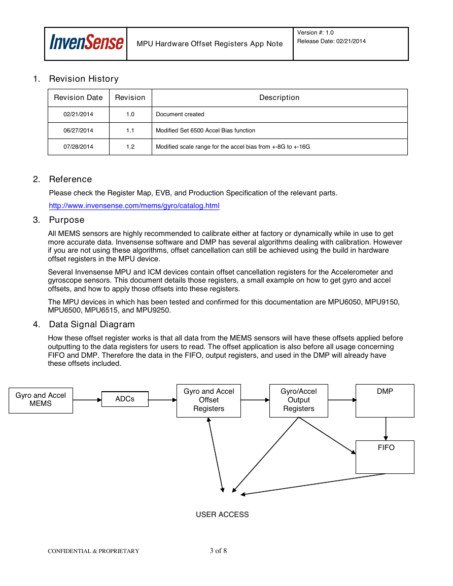
How these offset register works is that all data from the MEMS sensors will have these offsets applied before
outputting to the data registers for users to read. The offset application is also before all usage concerning
FIFO and DMP. Therefore the data in the FIFO, output registers, and used in the DMP will already have
these offsets included.
Gyro and Accel
MEMS
ADCs
Gyro and Accel
Offset
Registers
Gyro/Accel
Output
Registers
DMP
FIFO
USER ACCESS
CONFIDENTIAL & PROPRIETARY
3 of 8
�
MPU Hardware Offset Registers App Note
Version #: 1.0
Release Date: 02/21/2014
5. Finding the Offset Biases for Accel and Gyro
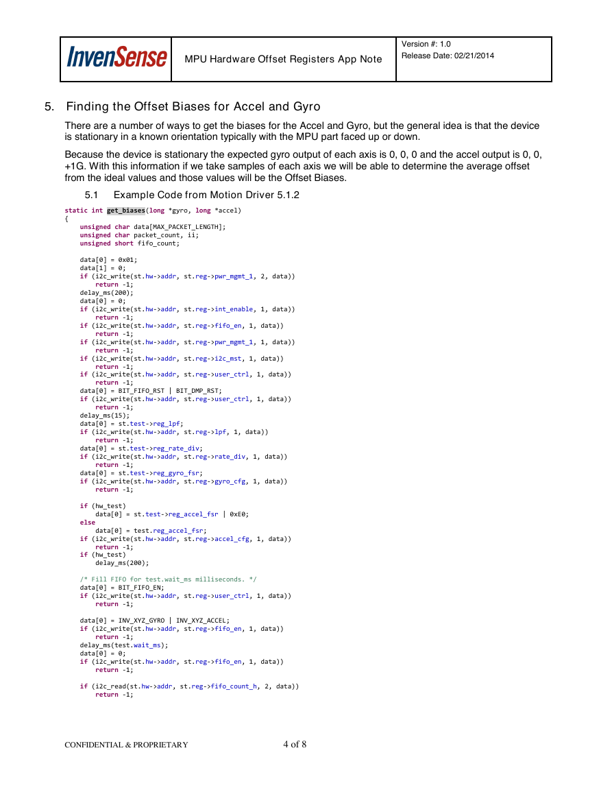
There are a number of ways to get the biases for the Accel and Gyro, but the general idea is that the device
is stationary in a known orientation typically with the MPU part faced up or down.
Because the device is stationary the expected gyro output of each axis is 0, 0, 0 and the accel output is 0, 0,
+1G. With this information if we take samples of each axis we will be able to determine the average offset
from the ideal values and those values will be the Offset Biases.
5.1 Example Code from Motion Driver 5.1.2
static int get_biases(long *gyro, long *accel)
{
unsigned char data[MAX_PACKET_LENGTH];
unsigned char packet_count, ii;
unsigned short fifo_count;
data[0] = 0x01;
data[1] = 0;
if (i2c_write(st.hw->addr, st.reg->pwr_mgmt_1, 2, data))
return -1;
delay_ms(200);
data[0] = 0;
if (i2c_write(st.hw->addr, st.reg->int_enable, 1, data))
return -1;
if (i2c_write(st.hw->addr, st.reg->fifo_en, 1, data))
return -1;
if (i2c_write(st.hw->addr, st.reg->pwr_mgmt_1, 1, data))
return -1;
if (i2c_write(st.hw->addr, st.reg->i2c_mst, 1, data))
return -1;
if (i2c_write(st.hw->addr, st.reg->user_ctrl, 1, data))
return -1;
data[0] = BIT_FIFO_RST | BIT_DMP_RST;
if (i2c_write(st.hw->addr, st.reg->user_ctrl, 1, data))
return -1;
delay_ms(15);
data[0] = st.test->reg_lpf;
if (i2c_write(st.hw->addr, st.reg->lpf, 1, data))
return -1;
data[0] = st.test->reg_rate_div;
if (i2c_write(st.hw->addr, st.reg->rate_div, 1, data))
return -1;
data[0] = st.test->reg_gyro_fsr;
if (i2c_write(st.hw->addr, st.reg->gyro_cfg, 1, data))
return -1;
if (hw_test)
data[0] = st.test->reg_accel_fsr | 0xE0;
else
data[0] = test.reg_accel_fsr;
if (i2c_write(st.hw->addr, st.reg->accel_cfg, 1, data))
return -1;
if (hw_test)
delay_ms(200);
/* Fill FIFO for test.wait_ms milliseconds. */
data[0] = BIT_FIFO_EN;
if (i2c_write(st.hw->addr, st.reg->user_ctrl, 1, data))
return -1;
data[0] = INV_XYZ_GYRO | INV_XYZ_ACCEL;
if (i2c_write(st.hw->addr, st.reg->fifo_en, 1, data))
return -1;
delay_ms(test.wait_ms);
data[0] = 0;
if (i2c_write(st.hw->addr, st.reg->fifo_en, 1, data))
return -1;
if (i2c_read(st.hw->addr, st.reg->fifo_count_h, 2, data))
return -1;
CONFIDENTIAL & PROPRIETARY
4 of 8
�
MPU Hardware Offset Registers App Note
Version #: 1.0
Release Date: 02/21/2014
fifo_count = (data[0] << 8) | data[1];
packet_count = fifo_count / MAX_PACKET_LENGTH;
gyro[0] = gyro[1] = gyro[2] = 0;
accel[0] = accel[1] = accel[2] = 0;
for (ii = 0; ii < packet_count; ii++) {
short accel_cur[3], gyro_cur[3];
if (i2c_read(st.hw->addr, st.reg->fifo_r_w, MAX_PACKET_LENGTH, data))
return -1;
accel_cur[0] = ((short)data[0] << 8) | data[1];
accel_cur[1] = ((short)data[2] << 8) | data[3];
accel_cur[2] = ((short)data[4] << 8) | data[5];
accel[0] += (long)accel_cur[0];
accel[1] += (long)accel_cur[1];
accel[2] += (long)accel_cur[2];
gyro_cur[0] = (((short)data[6] << 8) | data[7]);
gyro_cur[1] = (((short)data[8] << 8) | data[9]);
gyro_cur[2] = (((short)data[10] << 8) | data[11]);
gyro[0] += (long)gyro_cur[0];
gyro[1] += (long)gyro_cur[1];
gyro[2] += (long)gyro_cur[2];
}
gyro[0] = (long)(((long long)gyro[0]) / test.gyro_sens / packet_count);
gyro[1] = (long)(((long long)gyro[1]) / test.gyro_sens / packet_count);
gyro[2] = (long)(((long long)gyro[2]) / test.gyro_sens / packet_count);
accel[0] = (long)(((long long)accel[0]) / test.accel_sens /
packet_count);
accel[1] = (long)(((long long)accel[1]) / test.accel_sens /
packet_count);
accel[2] = (long)(((long long)accel[2]) / test.accel_sens /
packet_count);
/* remove gravity from the accel Z */
if (accel[2] > 0L)
accel[2] -= test.accel_sens;
else
accel[2] += test.accel_sens;
return 0;
}
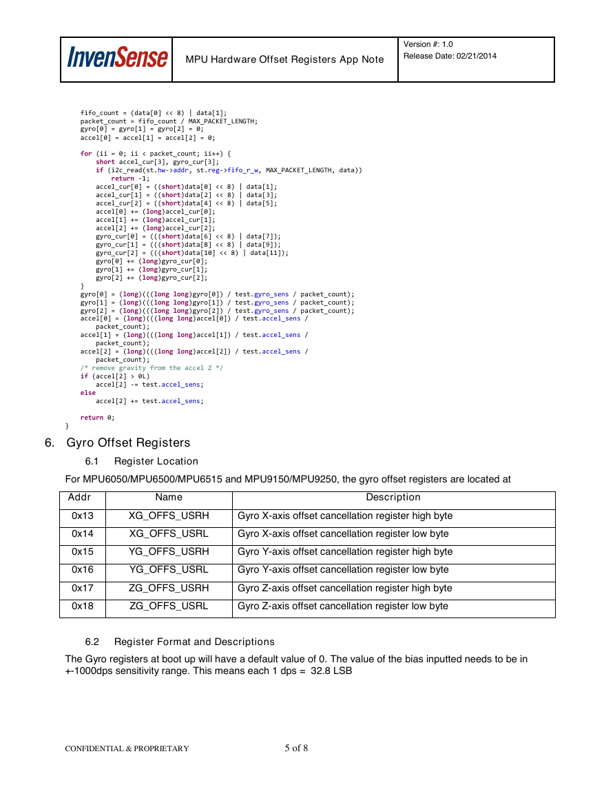
6. Gyro Offset Registers
6.1 Register Location
For MPU6050/MPU6500/MPU6515 and MPU9150/MPU9250, the gyro offset registers are located at
Addr
Name
Description
0x13
0x14
0x15
0x16
0x17
0x18
XG_OFFS_USRH
Gyro X-axis offset cancellation register high byte
XG_OFFS_USRL
Gyro X-axis offset cancellation register low byte
YG_OFFS_USRH
Gyro Y-axis offset cancellation register high byte
YG_OFFS_USRL
Gyro Y-axis offset cancellation register low byte
ZG_OFFS_USRH
Gyro Z-axis offset cancellation register high byte
ZG_OFFS_USRL
Gyro Z-axis offset cancellation register low byte
6.2 Register Format and Descriptions
The Gyro registers at boot up will have a default value of 0. The value of the bias inputted needs to be in
+-1000dps sensitivity range. This means each 1 dps = 32.8 LSB
CONFIDENTIAL & PROPRIETARY
5 of 8
�
MPU Hardware Offset Registers App Note
Version #: 1.0
Release Date: 02/21/2014
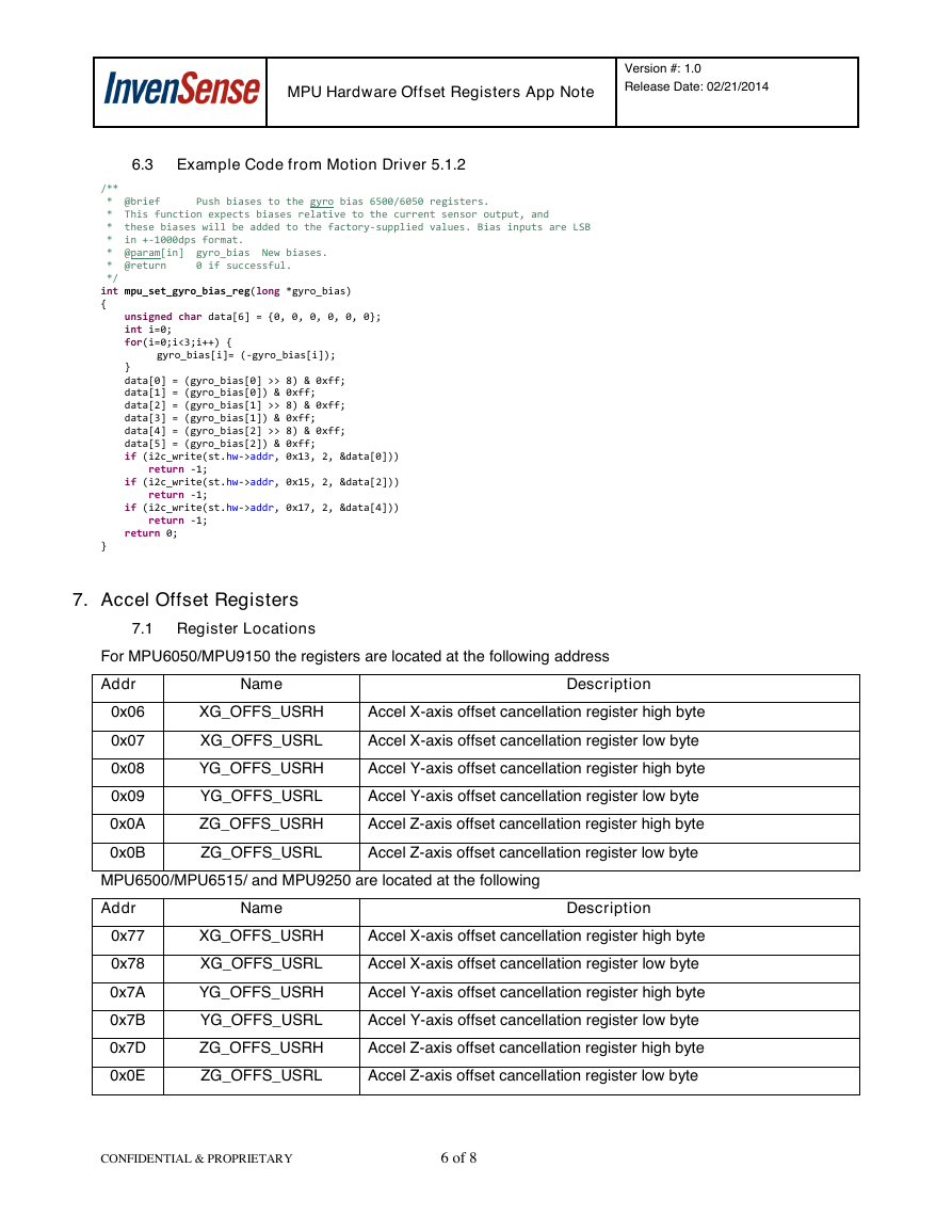
6.3 Example Code from Motion Driver 5.1.2
gyro_bias[i]= (-gyro_bias[i]);
/**
* @brief Push biases to the gyro bias 6500/6050 registers.
* This function expects biases relative to the current sensor output, and
* these biases will be added to the factory-supplied values. Bias inputs are LSB
* in +-1000dps format.
* @param[in] gyro_bias New biases.
* @return 0 if successful.
*/
int mpu_set_gyro_bias_reg(long *gyro_bias)
{
unsigned char data[6] = {0, 0, 0, 0, 0, 0};
int i=0;
for(i=0;i<3;i++) {
}
data[0] = (gyro_bias[0] >> 8) & 0xff;
data[1] = (gyro_bias[0]) & 0xff;
data[2] = (gyro_bias[1] >> 8) & 0xff;
data[3] = (gyro_bias[1]) & 0xff;
data[4] = (gyro_bias[2] >> 8) & 0xff;
data[5] = (gyro_bias[2]) & 0xff;
if (i2c_write(st.hw->addr, 0x13, 2, &data[0]))
return -1;
if (i2c_write(st.hw->addr, 0x15, 2, &data[2]))
return -1;
if (i2c_write(st.hw->addr, 0x17, 2, &data[4]))
return -1;
return 0;
}
7. Accel Offset Registers
7.1 Register Locations
For MPU6050/MPU9150 the registers are located at the following address
Addr
Name
Description
0x06
0x07
0x08
0x09
0x0A
0x0B
XG_OFFS_USRH
Accel X-axis offset cancellation register high byte
XG_OFFS_USRL
Accel X-axis offset cancellation register low byte
YG_OFFS_USRH
Accel Y-axis offset cancellation register high byte
YG_OFFS_USRL
Accel Y-axis offset cancellation register low byte
ZG_OFFS_USRH
Accel Z-axis offset cancellation register high byte
ZG_OFFS_USRL
Accel Z-axis offset cancellation register low byte
MPU6500/MPU6515/ and MPU9250 are located at the following
Addr
Name
Description
0x77
0x78
0x7A
0x7B
0x7D
0x0E
XG_OFFS_USRH
Accel X-axis offset cancellation register high byte
XG_OFFS_USRL
Accel X-axis offset cancellation register low byte
YG_OFFS_USRH
Accel Y-axis offset cancellation register high byte
YG_OFFS_USRL
Accel Y-axis offset cancellation register low byte
ZG_OFFS_USRH
Accel Z-axis offset cancellation register high byte
ZG_OFFS_USRL
Accel Z-axis offset cancellation register low byte
CONFIDENTIAL & PROPRIETARY
6 of 8
�
MPU Hardware Offset Registers App Note
Version #: 1.0
Release Date: 02/21/2014
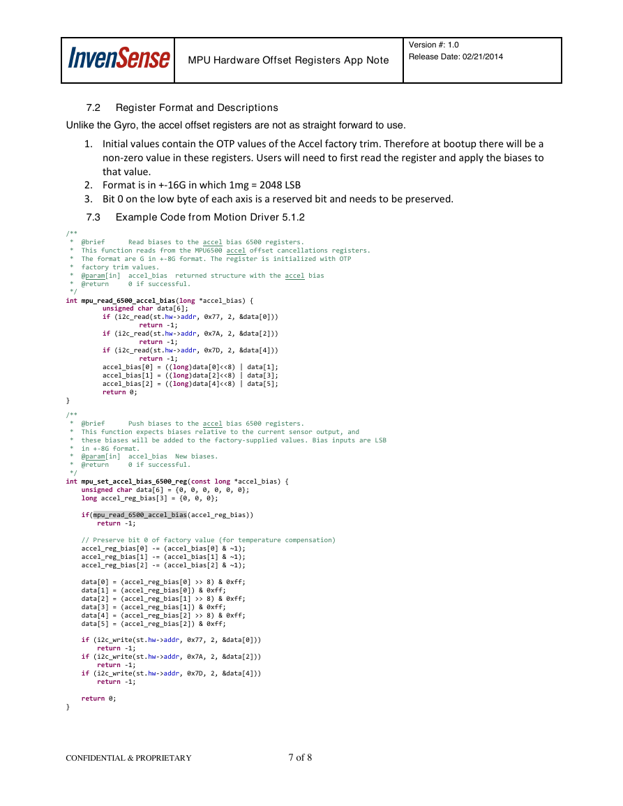
7.2 Register Format and Descriptions
Unlike the Gyro, the accel offset registers are not as straight forward to use.
1.
Initial values contain the OTP values of the Accel factory trim. Therefore at bootup there will be a
non-zero value in these registers. Users will need to first read the register and apply the biases to
that value.
2. Format is in +-16G in which 1mg = 2048 LSB
3. Bit 0 on the low byte of each axis is a reserved bit and needs to be preserved.
7.3 Example Code from Motion Driver 5.1.2
/**
* @brief Read biases to the accel bias 6500 registers.
* This function reads from the MPU6500 accel offset cancellations registers.
* The format are G in +-8G format. The register is initialized with OTP
* factory trim values.
* @param[in] accel_bias returned structure with the accel bias
* @return 0 if successful.
*/
int mpu_read_6500_accel_bias(long *accel_bias) {
}
unsigned char data[6];
if (i2c_read(st.hw->addr, 0x77, 2, &data[0]))
if (i2c_read(st.hw->addr, 0x7A, 2, &data[2]))
if (i2c_read(st.hw->addr, 0x7D, 2, &data[4]))
accel_bias[0] = ((long)data[0]<<8) | data[1];
accel_bias[1] = ((long)data[2]<<8) | data[3];
accel_bias[2] = ((long)data[4]<<8) | data[5];
return 0;
return -1;
return -1;
return -1;
/**
* @brief Push biases to the accel bias 6500 registers.
* This function expects biases relative to the current sensor output, and
* these biases will be added to the factory-supplied values. Bias inputs are LSB
* in +-8G format.
* @param[in] accel_bias New biases.
* @return 0 if successful.
*/
int mpu_set_accel_bias_6500_reg(const long *accel_bias) {
unsigned char data[6] = {0, 0, 0, 0, 0, 0};
long accel_reg_bias[3] = {0, 0, 0};
if(mpu_read_6500_accel_bias(accel_reg_bias))
return -1;
// Preserve bit 0 of factory value (for temperature compensation)
accel_reg_bias[0] -= (accel_bias[0] & ~1);
accel_reg_bias[1] -= (accel_bias[1] & ~1);
accel_reg_bias[2] -= (accel_bias[2] & ~1);
data[0] = (accel_reg_bias[0] >> 8) & 0xff;
data[1] = (accel_reg_bias[0]) & 0xff;
data[2] = (accel_reg_bias[1] >> 8) & 0xff;
data[3] = (accel_reg_bias[1]) & 0xff;
data[4] = (accel_reg_bias[2] >> 8) & 0xff;
data[5] = (accel_reg_bias[2]) & 0xff;
if (i2c_write(st.hw->addr, 0x77, 2, &data[0]))
return -1;
if (i2c_write(st.hw->addr, 0x7A, 2, &data[2]))
return -1;
if (i2c_write(st.hw->addr, 0x7D, 2, &data[4]))
return -1;
return 0;
}
CONFIDENTIAL & PROPRIETARY
7 of 8
�
MPU Hardware Offset Registers App Note
Version #: 1.0
Release Date: 02/21/2014
8. Misc
Bias offsets once inputted into the Offset Cancellation Registers will immediate take into effect. However
after power off and on the values will need to be reloaded back into these registers. It is recommended that
the bias values are saved so that can be easily reapplied after boot up.
CONFIDENTIAL & PROPRIETARY
8 of 8
�


 2023年江西萍乡中考道德与法治真题及答案.doc
 2012年重庆南川中考生物真题及答案.doc
 2013年江西师范大学地理学综合及文艺理论基础考研真题.doc
 2020年四川甘孜小升初语文真题及答案I卷.doc
 2020年注册岩土工程师专业基础考试真题及答案.doc
 2023-2024学年福建省厦门市九年级上学期数学月考试题及答案.doc
 2021-2022学年辽宁省沈阳市大东区九年级上学期语文期末试题及答案.doc
 2022-2023学年北京东城区初三第一学期物理期末试卷及答案.doc
 2018上半年江西教师资格初中地理学科知识与教学能力真题及答案.doc
 2012年河北国家公务员申论考试真题及答案-省级.doc
 2020-2021学年江苏省扬州市江都区邵樊片九年级上学期数学第一次质量检测试题及答案.doc
 2022下半年黑龙江教师资格证中学综合素质真题及答案.doc