Genesys Logic, Inc.
GL3224
USB 3.0 Dual/Single LUN
Memory Card Reader Controller
Datasheet
Revision 1.08
Jul. 21, 2017
�
GL3224 Datasheet
Copyright
Copyright © 2017 Genesys Logic, Inc. All rights reserved. No part of the materials shall be reproduced in any
form or by any means without prior written consent of Genesys Logic, Inc.
Ownership and Title
Genesys Logic, Inc. owns and retains of its right, title and interest in and to all materials provided herein.
Genesys Logic, Inc. reserves all rights, including, but not limited to, all patent rights, trademarks, copyrights and
any other propriety rights. No license is granted hereunder.
Disclaimer
All Materials are provided “as is”. Genesys Logic, Inc. makes no warranties, express, implied or otherwise,
regarding their accuracy, merchantability, fitness for any particular purpose, and non-infringement of intellectual
property. In no event shall Genesys Logic, Inc. be liable for any damages, including, without limitation, any
direct, indirect, consequential, or incidental damages. The materials may contain errors or omissions. Genesys
Logic, Inc. may make changes to the materials or to the products described herein at anytime without notice.
Genesys Logic, Inc.
12F., No. 205, Sec. 3, Beixin Rd., Xindian Dist. 231,
New Taipei City, Taiwan
Tel : (886-2) 8913-1888
Fax : (886-2) 6629-6168
http ://www.genesyslogic.com
© 2017 Genesys Logic, Inc. - All rights reserved. Page 2
GLI Confidential
�
GL3224 Datasheet
Revision History
Revision
Date
Description
1.00
1.01
1.02
1.03
1.04
1.05
1.06
1.07
1.08
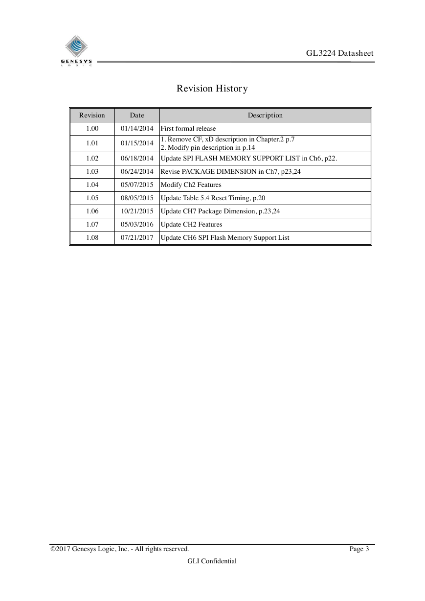
01/14/2014 First formal release
01/15/2014
1. Remove CF, xD description in Chapter.2 p.7
2. Modify pin description in p.14
06/18/2014 Update SPI FLASH MEMORY SUPPORT LIST in Ch6, p22.
06/24/2014 Revise PACKAGE DIMENSION in Ch7, p23,24
05/07/2015 Modify Ch2 Features
08/05/2015 Update Table 5.4 Reset Timing, p.20
10/21/2015 Update CH7 Package Dimension, p.23,24
05/03/2016 Update CH2 Features
07/21/2017 Update CH6 SPI Flash Memory Support List
© 2017 Genesys Logic, Inc. - All rights reserved. Page 3
GLI Confidential
�
GL3224 Datasheet
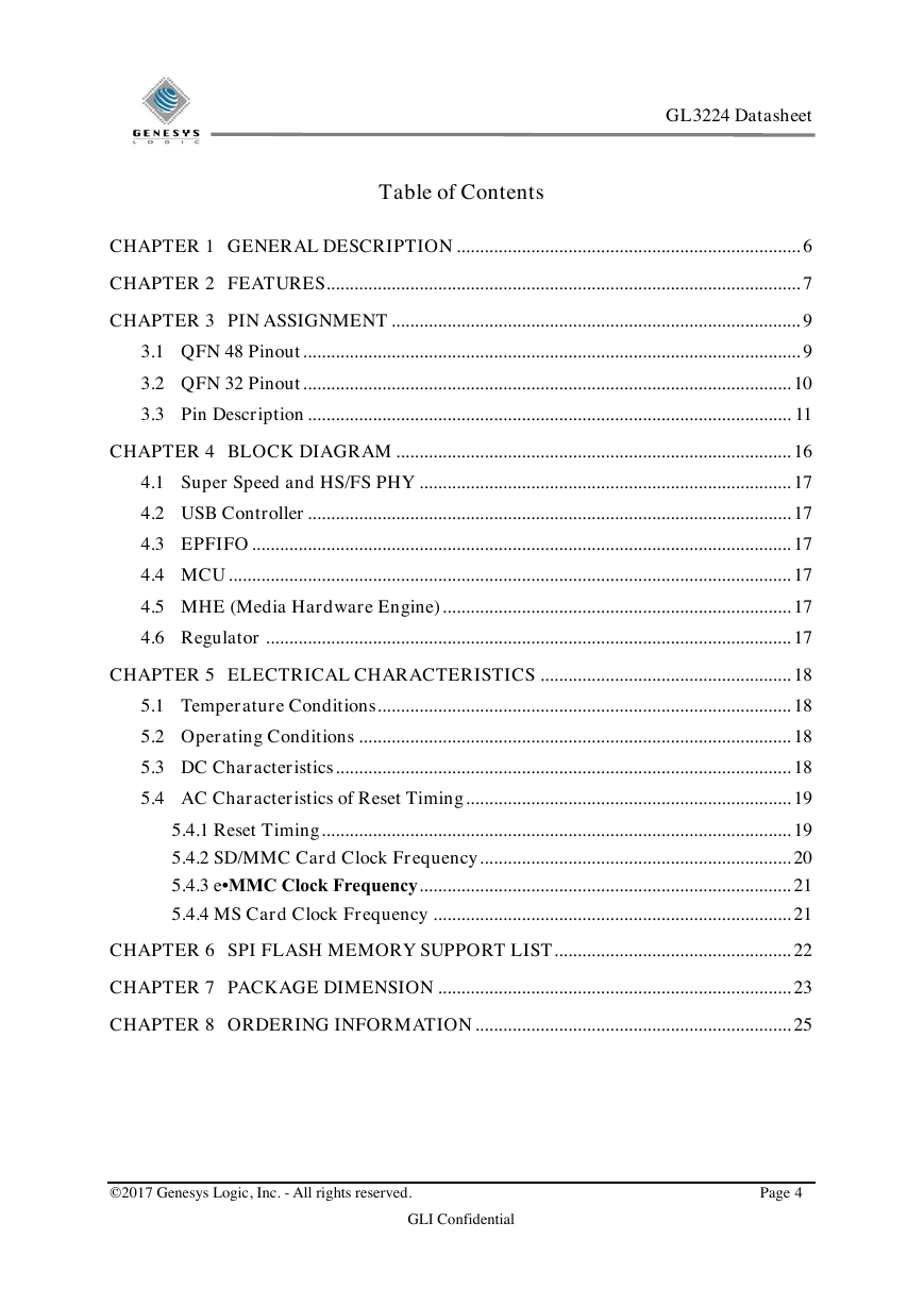
Table of Contents
CHAPTER 1 GENERAL DESCRIPTION .......................................................................... 6
CHAPTER 2 FEATURES...................................................................................................... 7
CHAPTER 3 PIN ASSIGNMENT ........................................................................................ 9
3.1 QFN 48 Pinout ........................................................................................................... 9
3.2 QFN 32 Pinout ......................................................................................................... 10
3.3 Pin Description ........................................................................................................ 11
CHAPTER 4 BLOCK DIAGRAM ..................................................................................... 16
4.1 Super Speed and HS/FS PHY ................................................................................ 17
4.2 USB Controller ........................................................................................................ 17
4.3 EPFIFO .................................................................................................................... 17
4.4 MCU ......................................................................................................................... 17
4.5 MHE (Media Hardware Engine) ........................................................................... 17
4.6 Regulator ................................................................................................................. 17
CHAPTER 5 ELECTRICAL CHARACTERISTICS ...................................................... 18
5.1 Temperature Conditions ......................................................................................... 18
5.2 Operating Conditions ............................................................................................. 18
5.3 DC Characteristics .................................................................................................. 18
5.4 AC Characteristics of Reset Timing ...................................................................... 19
5.4.1 Reset Timing ..................................................................................................... 19
5.4.2 SD/MMC Card Clock Frequency ................................................................... 20
5.4.3 e•MMC Clock Frequency ................................................................................ 21
5.4.4 MS Card Clock Frequency ............................................................................. 21
CHAPTER 6 SPI FLASH MEMORY SUPPORT LIST ................................................... 22
CHAPTER 7 PACKAGE DIMENSION ............................................................................ 23
CHAPTER 8 ORDERING INFORMATION .................................................................... 25
© 2017 Genesys Logic, Inc. - All rights reserved. Page 4
GLI Confidential
�
GL3224 Datasheet
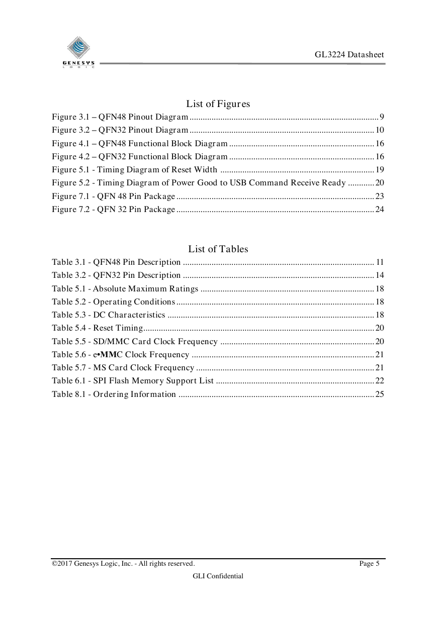
List of Figures
Figure 3.1 – QFN48 Pinout Diagram ...................................................................................... 9
Figure 3.2 – QFN32 Pinout Diagram .................................................................................... 10
Figure 4.1 – QFN48 Functional Block Diagram .................................................................. 16
Figure 4.2 – QFN32 Functional Block Diagram .................................................................. 16
Figure 5.1 - Timing Diagram of Reset Width ...................................................................... 19
Figure 5.2 - Timing Diagram of Power Good to USB Command Receive Ready ............ 20
Figure 7.1 - QFN 48 Pin Package .......................................................................................... 23
Figure 7.2 - QFN 32 Pin Package .......................................................................................... 24
List of Tables
Table 3.1 - QFN48 Pin Description ....................................................................................... 11
Table 3.2 - QFN32 Pin Description ....................................................................................... 14
Table 5.1 - Absolute Maximum Ratings ............................................................................... 18
Table 5.2 - Operating Conditions .......................................................................................... 18
Table 5.3 - DC Characteristics .............................................................................................. 18
Table 5.4 - Reset Timing......................................................................................................... 20
Table 5.5 - SD/MMC Card Clock Frequency ...................................................................... 20
Table 5.6 - e•MMC Clock Frequency ................................................................................... 21
Table 5.7 - MS Card Clock Frequency ................................................................................. 21
Table 6.1 - SPI Flash Memory Support List ........................................................................ 22
Table 8.1 - Ordering Information ......................................................................................... 25
© 2017 Genesys Logic, Inc. - All rights reserved. Page 5
GLI Confidential
�
GL3224 Datasheet
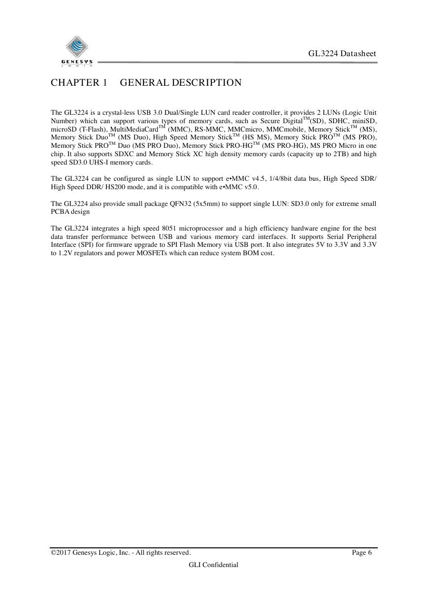
CHAPTER 1 GENERAL DESCRIPTION
The GL3224 is a crystal-less USB 3.0 Dual/Single LUN card reader controller, it provides 2 LUNs (Logic Unit
Number) which can support various types of memory cards, such as Secure DigitalTM(SD), SDHC, miniSD,
microSD (T-Flash), MultiMediaCardTM (MMC), RS-MMC, MMCmicro, MMCmobile, Memory StickTM (MS),
Memory Stick DuoTM (MS Duo), High Speed Memory StickTM (HS MS), Memory Stick PROTM (MS PRO),
Memory Stick PROTM Duo (MS PRO Duo), Memory Stick PRO-HGTM (MS PRO-HG), MS PRO Micro in one
chip. It also supports SDXC and Memory Stick XC high density memory cards (capacity up to 2TB) and high
speed SD3.0 UHS-I memory cards.
The GL3224 can be configured as single LUN to support e•MMC v4.5, 1/4/8bit data bus, High Speed SDR/
High Speed DDR/ HS200 mode, and it is compatible with e•MMC v5.0.
The GL3224 also provide small package QFN32 (5x5mm) to support single LUN: SD3.0 only for extreme small
PCBA design
The GL3224 integrates a high speed 8051 microprocessor and a high efficiency hardware engine for the best
data transfer performance between USB and various memory card interfaces. It supports Serial Peripheral
Interface (SPI) for firmware upgrade to SPI Flash Memory via USB port. It also integrates 5V to 3.3V and 3.3V
to 1.2V regulators and power MOSFETs which can reduce system BOM cost.
© 2017 Genesys Logic, Inc. - All rights reserved. Page 6
GLI Confidential
�
GL3224 Datasheet
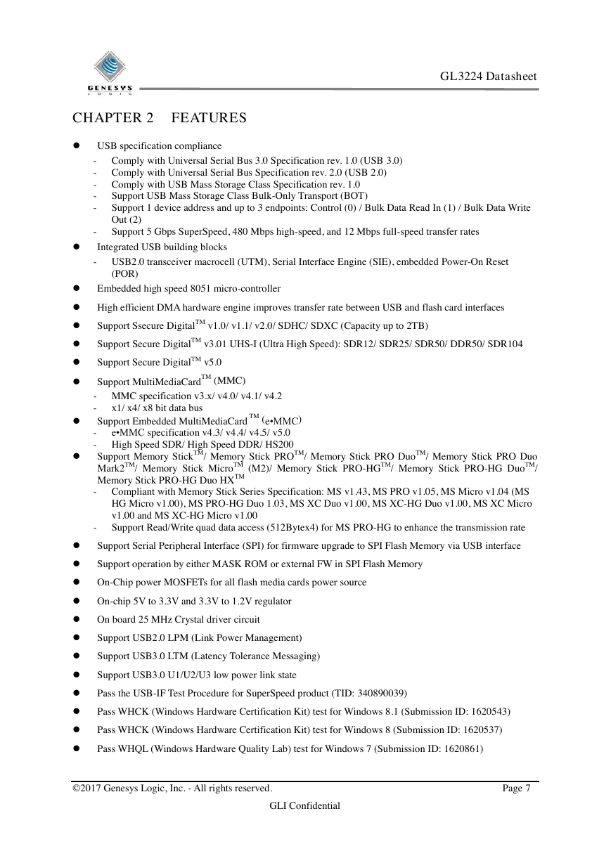
CHAPTER 2 FEATURES
USB specification compliance
- Comply with Universal Serial Bus 3.0 Specification rev. 1.0 (USB 3.0)
- Comply with Universal Serial Bus Specification rev. 2.0 (USB 2.0)
- Comply with USB Mass Storage Class Specification rev. 1.0
-
-
Support USB Mass Storage Class Bulk-Only Transport (BOT)
Support 1 device address and up to 3 endpoints: Control (0) / Bulk Data Read In (1) / Bulk Data Write
Out (2)
Support 5 Gbps SuperSpeed, 480 Mbps high-speed, and 12 Mbps full-speed transfer rates
-
Integrated USB building blocks
- USB2.0 transceiver macrocell (UTM), Serial Interface Engine (SIE), embedded Power-On Reset
(POR)
Embedded high speed 8051 micro-controller
High efficient DMA hardware engine improves transfer rate between USB and flash card interfaces
Support Ssecure DigitalTM v1.0/ v1.1/ v2.0/ SDHC/ SDXC (Capacity up to 2TB)
Support Secure DigitalTM v3.01 UHS-I (Ultra High Speed): SDR12/ SDR25/ SDR50/ DDR50/ SDR104
Support Secure DigitalTM v5.0
-
TM (MMC)
TM (e•MMC)
x1/ x4/ x8 bit data bus
Support MultiMediaCard
- MMC specification v3.x/ v4.0/ v4.1/ v4.2
-
Support Embedded MultiMediaCard
-
e•MMC specification v4.3/ v4.4/ v4.5/ v5.0
- High Speed SDR/ High Speed DDR/ HS200
Support Memory StickTM/ Memory Stick PROTM/ Memory Stick PRO DuoTM/ Memory Stick PRO Duo
Mark2TM/ Memory Stick MicroTM (M2)/ Memory Stick PRO-HGTM/ Memory Stick PRO-HG DuoTM/
Memory Stick PRO-HG Duo HXTM
- Compliant with Memory Stick Series Specification: MS v1.43, MS PRO v1.05, MS Micro v1.04 (MS
HG Micro v1.00), MS PRO-HG Duo 1.03, MS XC Duo v1.00, MS XC-HG Duo v1.00, MS XC Micro
v1.00 and MS XC-HG Micro v1.00
Support Read/Write quad data access (512Bytex4) for MS PRO-HG to enhance the transmission rate
Support Serial Peripheral Interface (SPI) for firmware upgrade to SPI Flash Memory via USB interface
Support operation by either MASK ROM or external FW in SPI Flash Memory
On-Chip power MOSFETs for all flash media cards power source
On-chip 5V to 3.3V and 3.3V to 1.2V regulator
On board 25 MHz Crystal driver circuit
Support USB2.0 LPM (Link Power Management)
Support USB3.0 LTM (Latency Tolerance Messaging)
Support USB3.0 U1/U2/U3 low power link state
Pass the USB-IF Test Procedure for SuperSpeed product (TID: 340890039)
Pass WHCK (Windows Hardware Certification Kit) test for Windows 8.1 (Submission ID: 1620543)
Pass WHCK (Windows Hardware Certification Kit) test for Windows 8 (Submission ID: 1620537)
Pass WHQL (Windows Hardware Quality Lab) test for Windows 7 (Submission ID: 1620861)
© 2017 Genesys Logic, Inc. - All rights reserved. Page 7
GLI Confidential
�
GL3224 Datasheet
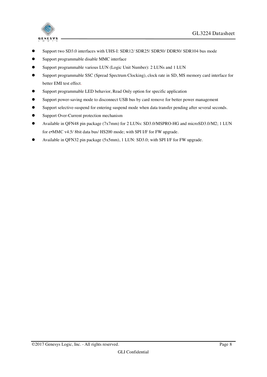
Support two SD3.0 interfaces with UHS-I: SDR12/ SDR25/ SDR50/ DDR50/ SDR104 bus mode
Support programmable disable MMC interface
Support programmable various LUN (Logic Unit Number): 2 LUNs and 1 LUN
Support programmable SSC (Spread Spectrum Clocking), clock rate in SD, MS memory card interface for
better EMI test effect.
Support programmable LED behavior, Read Only option for specific application
Support power-saving mode to disconnect USB bus by card remove for better power management
Support selective-suspend for entering suspend mode when data transfer pending after several seconds.
Support Over-Current protection mechanism
Available in QFN48 pin package (7x7mm) for 2 LUNs: SD3.0/MSPRO-HG and microSD3.0/M2; 1 LUN
for e•MMC v4.5/ 8bit data bus/ HS200 mode; with SPI I/F for FW upgrade.
Available in QFN32 pin package (5x5mm), 1 LUN: SD3.0; with SPI I/F for FW upgrade.
© 2017 Genesys Logic, Inc. - All rights reserved. Page 8
GLI Confidential
�


 2023年江西萍乡中考道德与法治真题及答案.doc
 2012年重庆南川中考生物真题及答案.doc
 2013年江西师范大学地理学综合及文艺理论基础考研真题.doc
 2020年四川甘孜小升初语文真题及答案I卷.doc
 2020年注册岩土工程师专业基础考试真题及答案.doc
 2023-2024学年福建省厦门市九年级上学期数学月考试题及答案.doc
 2021-2022学年辽宁省沈阳市大东区九年级上学期语文期末试题及答案.doc
 2022-2023学年北京东城区初三第一学期物理期末试卷及答案.doc
 2018上半年江西教师资格初中地理学科知识与教学能力真题及答案.doc
 2012年河北国家公务员申论考试真题及答案-省级.doc
 2020-2021学年江苏省扬州市江都区邵樊片九年级上学期数学第一次质量检测试题及答案.doc
 2022下半年黑龙江教师资格证中学综合素质真题及答案.doc