K9HBG08U1M
K9LAG08U0M
K9MCG08U5M
Advance
FLASH MEMORY
K9XXG08UXM
INFORMATION IN THIS DOCUMENT IS PROVIDED IN RELATION TO SAMSUNG PRODUCTS,
AND IS SUBJECT TO CHANGE WITHOUT NOTICE.
NOTHING IN THIS DOCUMENT SHALL BE CONSTRUED AS GRANTING ANY LICENSE,
EXPRESS OR IMPLIED, BY ESTOPPEL OR OTHERWISE,
TO ANY INTELLECTUAL PROPERTY RIGHTS IN SAMSUNG PRODUCTS OR TECHNOLOGY. ALL
INFORMATION IN THIS DOCUMENT IS PROVIDED
ON AS "AS IS" BASIS WITHOUT GUARANTEE OR WARRANTY OF ANY KIND.
1. For updates or additional information about Samsung products, contact your nearest Samsung office.
2. Samsung products are not intended for use in life support, critical care, medical, safety equipment, or similar
applications where Product failure could result in loss of life or personal or physical harm, or any military or
defense application, or any governmental procurement to which special terms or provisions may apply.
* Samsung Electronics reserves the right to change products or specification without notice.
1
www.DataSheet4U.com�
K9HBG08U1M
K9LAG08U0M
K9MCG08U5M
Document Title
2G x 8 Bit / 4G x 8 Bit NAND Flash Memory
Revision History
Revision No
History
0.0
0.1
0.2
0.3
0.4
0.5
0.6
0.7
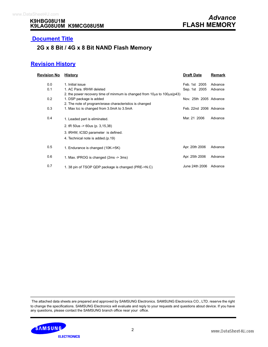
1. Initial issue
1. AC Para. tRHW deleted
2. the power recovery time of minmum is changed from 10µs to 100µs(p43)
1. DSP package is added
2. The note of program/erase characteristics is changed
1. Max Icc is changed from 3.0mA to 3.5mA
1. Leaded part is eliminated.
2. tR 50us -> 60us (p. 3,15,38)
3. tRHW, tCSD parameter is defined.
4. Technical note is added.(p.19)
1. Endurance is changed (10K->5K)
1. Max. tPROG is changed (2ms -> 3ms)
1. 38 pin of TSOP QDP package is changed (PRE->N.C)
Advance
FLASH MEMORY
Draft Date
Remark
Feb. 1st 2005
Sep. 1st 2005
Advance
Advance
Nov. 25th 2005
Advance
Feb. 22nd 2006
Advance
Mar. 21 2006
Advance
Apr. 20th 2006
Advance
Apr. 25th 2006
Advance
June 24th 2006
Advance
The attached data sheets are prepared and approved by SAMSUNG Electronics. SAMSUNG Electronics CO., LTD. reserve the right
to change the specifications. SAMSUNG Electronics will evaluate and reply to your requests and questions about device. If you have
any questions, please contact the SAMSUNG branch office near your office.
2
www.DataSheet4U.com�
K9HBG08U1M
K9LAG08U0M
K9MCG08U5M
2G x 8 Bit / 4G x 8 Bit NAND Flash Memory
PRODUCT LIST
Part Number
Vcc Range
Organization
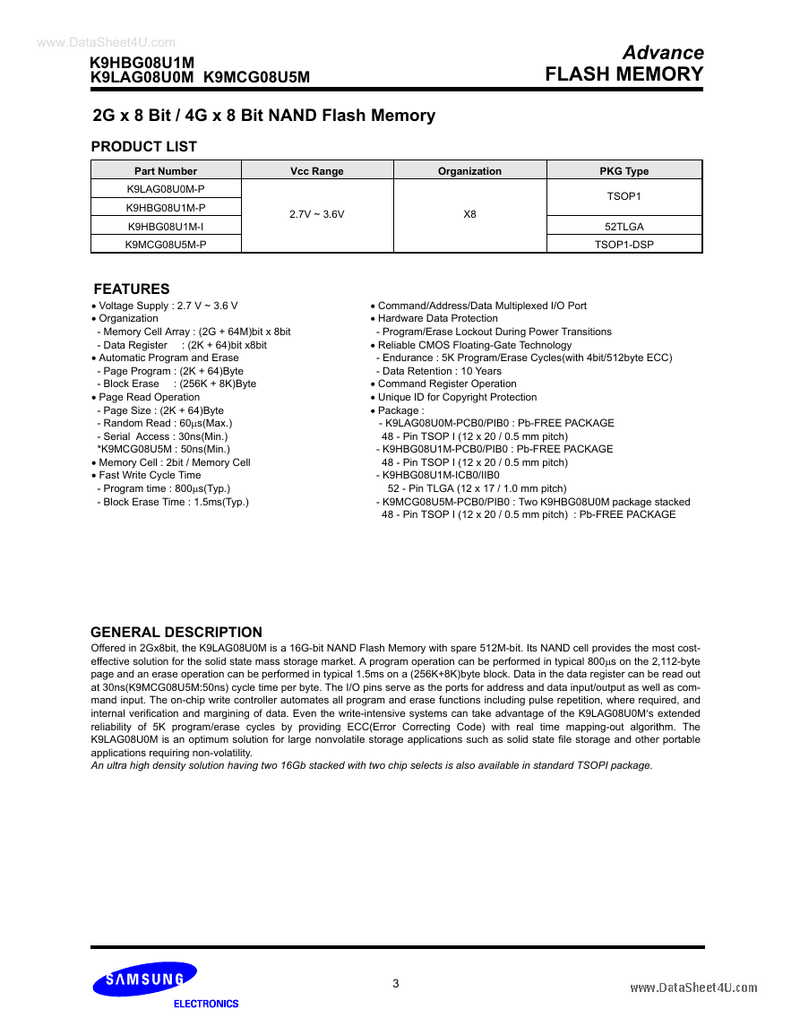
K9LAG08U0M-P
K9HBG08U1M-P
K9HBG08U1M-I
K9MCG08U5M-P
2.7V ~ 3.6V
X8
Advance
FLASH MEMORY
PKG Type
TSOP1
52TLGA
TSOP1-DSP
FEATURES
• Voltage Supply : 2.7 V ~ 3.6 V
• Organization
- Memory Cell Array : (2G + 64M)bit x 8bit
- Data Register : (2K + 64)bit x8bit
• Automatic Program and Erase
- Page Program : (2K + 64)Byte
- Block Erase : (256K + 8K)Byte
• Page Read Operation
- Page Size : (2K + 64)Byte
- Random Read : 60µs(Max.)
- Serial Access : 30ns(Min.)
*K9MCG08U5M : 50ns(Min.)
• Memory Cell : 2bit / Memory Cell
• Fast Write Cycle Time
- Program time : 800µs(Typ.)
- Block Erase Time : 1.5ms(Typ.)
• Command/Address/Data Multiplexed I/O Port
• Hardware Data Protection
- Program/Erase Lockout During Power Transitions
• Reliable CMOS Floating-Gate Technology
- Endurance : 5K Program/Erase Cycles(with 4bit/512byte ECC)
- Data Retention : 10 Years
• Command Register Operation
• Unique ID for Copyright Protection
• Package :
- K9LAG08U0M-PCB0/PIB0 : Pb-FREE PACKAGE
48 - Pin TSOP I (12 x 20 / 0.5 mm pitch)
- K9HBG08U1M-PCB0/PIB0 : Pb-FREE PACKAGE
48 - Pin TSOP I (12 x 20 / 0.5 mm pitch)
- K9HBG08U1M-ICB0/IIB0
52 - Pin TLGA (12 x 17 / 1.0 mm pitch)
- K9MCG08U5M-PCB0/PIB0 : Two K9HBG08U0M package stacked
48 - Pin TSOP I (12 x 20 / 0.5 mm pitch) : Pb-FREE PACKAGE
GENERAL DESCRIPTION
Offered in 2Gx8bit, the K9LAG08U0M is a 16G-bit NAND Flash Memory with spare 512M-bit. Its NAND cell provides the most cost-
effective solution for the solid state mass storage market. A program operation can be performed in typical 800µs on the 2,112-byte
page and an erase operation can be performed in typical 1.5ms on a (256K+8K)byte block. Data in the data register can be read out
at 30ns(K9MCG08U5M:50ns) cycle time per byte. The I/O pins serve as the ports for address and data input/output as well as com-
mand input. The on-chip write controller automates all program and erase functions including pulse repetition, where required, and
internal verification and margining of data. Even the write-intensive systems can take advantage of the K9LAG08U0M′s extended
reliability of 5K program/erase cycles by providing ECC(Error Correcting Code) with real time mapping-out algorithm. The
K9LAG08U0M is an optimum solution for large nonvolatile storage applications such as solid state file storage and other portable
applications requiring non-volatility.
An ultra high density solution having two 16Gb stacked with two chip selects is also available in standard TSOPI package.
3
www.DataSheet4U.com�
K9HBG08U1M
K9LAG08U0M
K9MCG08U5M
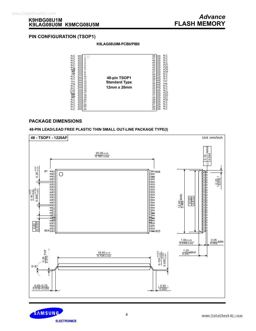
PIN CONFIGURATION (TSOP1)
Advance
FLASH MEMORY
K9LAG08U0M-PCB0/PIB0
48-pin TSOP1
Standard Type
12mm x 20mm
N.C
N.C
N.C
N.C
N.C
N.C
R/B
RE
CE
N.C
N.C
Vcc
Vss
N.C
N.C
CLE
ALE
WE
WP
N.C
N.C
N.C
N.C
N.C
1
2
3
4
5
6
7
8
9
10
11
12
13
14
15
16
17
18
19
20
21
22
23
24
48
47
46
45
44
43
42
41
40
39
38
37
36
35
34
33
32
31
30
29
28
27
26
25
N.C
N.C
N.C
N.C
I/O7
I/O6
I/O5
I/O4
N.C
N.C
N.C
Vcc
Vss
N.C
N.C
N.C
I/O3
I/O2
I/O1
I/O0
N.C
N.C
N.C
N.C
PACKAGE DIMENSIONS
48-PIN LEAD/LEAD FREE PLASTIC THIN SMALL OUT-LINE PACKAGE TYPE(I)
48 - TSOP1 - 1220AF
Unit :mm/Inch
20.00±0.20
0.787±0.008
18.40±0.10
0.724±0.004
#1
#24
P
Y
T
5
2
.
0
0
1
0
.
0
X
A
M
0
1
.
0
4
0
0
.
0
#48
#25
5
7
0
.
0
+
5
3
0
.
0
5
2
1
.
0
3
0
0
.
0
+
1
0
0
.
0
-
5
0
0
.
0
)
5
2
.
0
0
1
0
.
0
(
X
A
M
0
4
.
2
1
8
8
4
.
0
0
0
.
2
1
2
7
4
.
0
0.05 MIN
0.002
1.00±0.05
0.039±0.002
1.20 MAX
0.047
7
0
.
0
+
3
0
.
0
-
0
2
.
0
7
0
.
0
+
3
0
.
0
-
6
1
.
0
1
0
0
.
3
0
0
.
0
+
0
-
8
0
0
.
0
7
9
1
0
.
0
5
.
0
0
0~8°
0.45~0.75
0.018~0.030
(
0.50
0.020
)
4
www.DataSheet4U.com�
K9HBG08U1M
K9LAG08U0M
K9MCG08U5M
PIN CONFIGURATION (TSOP1)
K9HBG08U1M-PCB0/PIB0
Advance
FLASH MEMORY
N.C
N.C
N.C
N.C
N.C
R/B2
R/B1
RE
CE1
CE2
N.C
Vcc
Vss
N.C
N.C
CLE
ALE
WE
WP
N.C
N.C
N.C
N.C
N.C
1
2
3
4
5
6
7
8
9
10
11
12
13
14
15
16
17
18
19
20
21
22
23
24
48-pin TSOP1
Standard Type
12mm x 20mm
48
47
46
45
44
43
42
41
40
39
38
37
36
35
34
33
32
31
30
29
28
27
26
25
N.C
N.C
N.C
N.C
I/O7
I/O6
I/O5
I/O4
N.C
N.C
N.C
Vcc
Vss
N.C
N.C
N.C
I/O3
I/O2
I/O1
I/O0
N.C
N.C
N.C
N.C
PACKAGE DIMENSIONS
48-PIN LEAD/LEAD FREE PLASTIC THIN SMALL OUT-LINE PACKAGE TYPE(I)
48 - TSOP1 - 1220AF
Unit :mm/Inch
20.00±0.20
0.787±0.008
18.40±0.10
0.724±0.004
#1
#24
P
Y
T
5
2
.
0
0
1
0
.
0
X
A
M
0
1
.
0
4
0
0
.
0
#48
#25
5
7
0
.
0
+
5
3
0
.
0
5
2
1
.
0
3
0
0
.
0
+
1
0
0
.
0
-
5
0
0
.
0
)
5
2
.
0
0
1
0
.
0
(
X
A
M
0
4
.
2
1
8
8
4
.
0
0
0
.
2
1
2
7
4
.
0
0.02 MIN
0.002
1.00±0.05
0.039±0.002
1.20 MAX
0.047
7
0
.
0
+
3
0
.
0
-
0
2
.
0
7
0
.
0
+
3
0
.
0
-
6
1
.
0
1
0
0
.
3
0
0
.
0
+
0
-
8
0
0
.
0
7
9
1
0
.
0
5
.
0
0
0~8°
0.45~0.75
0.018~0.030
(
0.50
0.020
)
5
www.DataSheet4U.com�
K9HBG08U1M
K9LAG08U0M
K9MCG08U5M
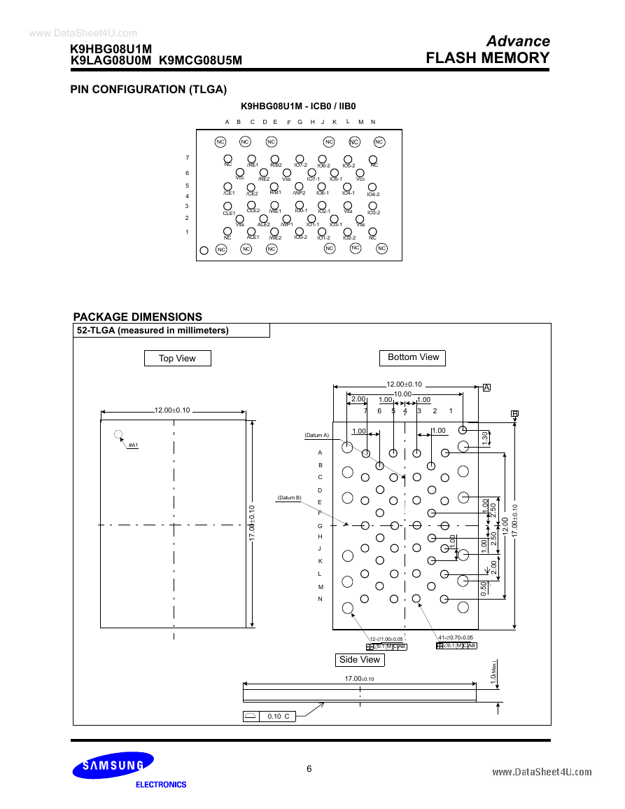
PIN CONFIGURATION (TLGA)
Advance
FLASH MEMORY
K9HBG08U1M - ICB0 / IIB0
A B
C D E
F G H J
K
L M N
NC
NC
NC
NC
NC
NC
NC
/RE1
R/B2
IO7-2
IO6-2
IO5-2
NC
Vcc
/RE2
Vss
IO7-1
IO5-1
Vcc
/CE1
/CE2
R/B1
/WP2
IO6-1
IO4-1
CLE1
CLE2
/WE1
IO0-1
IO2-1
Vss
Vss
ALE2
/WP1
IO1-1
IO3-1
Vss
IO4-2
IO3-2
NC
ALE1
/WE2
IO0-2
IO1-2
IO2-2
NC
NC
NC
NC
NC
NC
NC
7
6
5
4
3
2
1
PACKAGE DIMENSIONS
52-TLGA (measured in millimeters)
Top View
12.00±0.10
#A1
Bottom View
12.00±0.10
10.00
1.00
2.00
7 6 5 4 3 2 1
1.00
(Datum A)
1.00
1.00
(Datum B)
0
1
.
0
±
0
0
.
7
1
A
B
C
D
E
F
G
H
J
K
L
M
N
0.10 C
6
0
0
.
1
41-∅0.70±0.05
ABCM0.1
∅
12-∅1.00±0.05
∅
ABCM0.1
Side View
17.00±0.10
A
0
3
.
1
B
0
1
.
0
0
.
2
1
0
±
0
0
.
7
1
0
0
.
1
0
5
.
2
0
5
.
2
0
0
.
1
0
0
.
2
0
5
.
0
)
.
x
a
M
0
1
.
(
www.DataSheet4U.com�
K9HBG08U1M
K9LAG08U0M
K9MCG08U5M
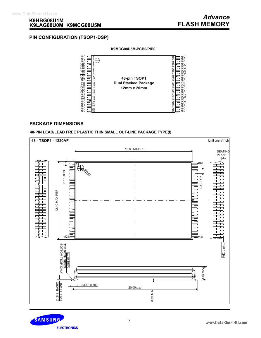
PIN CONFIGURATION (TSOP1-DSP)
K9MCG08U5M-PCB0/PIB0
Advance
FLASH MEMORY
N.C
N.C
N.C
R/B4
R/B3
R/B2
R/B1
RE
CE1
CE2
N.C
Vcc
Vss
CE3
CE4
CLE
ALE
WE
WP
N.C
N.C
N.C
N.C
N.C
1
2
3
4
5
6
7
8
9
10
11
12
13
14
15
16
17
18
19
20
21
22
23
24
48-pin TSOP1
Dual Stacked Package
12mm x 20mm
PACKAGE DIMENSIONS
48-PIN LEAD/LEAD FREE PLASTIC THIN SMALL OUT-LINE PACKAGE TYPE(I)
48 - TSOP1 - 1220AF
18.80 MAX REF
#1
Pin #
1
3
2
.
0
~
3
1
.
0
F
E
R
X
A
M
0
4
.
2
1
#24
T
Y
P
B
O
T
H
S
D
E
S
I
B
O
T
T
O
M
T
S
O
P
O
N
L
Y
(
0
.
1
0
)
A
I
C
S
A
B
)
9
4
2
.
0
(
E
N
A
L
P
E
G
A
G
0.399~0.600
20.00±0.20
I
N
M
2
0
.
0
7
48
47
46
45
44
43
42
41
40
39
38
37
36
35
34
33
32
31
30
29
28
27
26
25
N.C
N.C
N.C
N.C
I/O7
I/O6
I/O5
I/O4
N.C
N.C
N.C
Vcc
Vss
N.C
N.C
N.C
I/O3
I/O2
I/O1
I/O0
N.C
N.C
N.C
N.C
Unit :mm/Inch
SEATING
PLANE
-A-
(
0
.
1
0
)
A
#48
P
Y
T
0
5
.
0
#25
X
A
M
5
3
.
2
www.DataSheet4U.com�
K9HBG08U1M
K9LAG08U0M
K9MCG08U5M
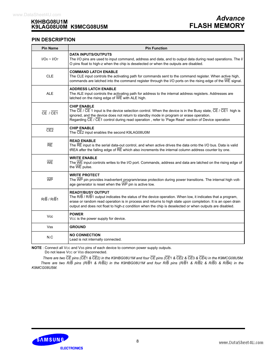
PIN DESCRIPTION
Advance
FLASH MEMORY
Pin Name
I/O0 ~ I/O7
CLE
ALE
CE / CE1
CE2
RE
WE
WP
Pin Function
DATA INPUTS/OUTPUTS
The I/O pins are used to input command, address and data, and to output data during read operations. The I/
O pins float to high-z when the chip is deselected or when the outputs are disabled.
COMMAND LATCH ENABLE
The CLE input controls the activating path for commands sent to the command register. When active high,
commands are latched into the command register through the I/O ports on the rising edge of the WE signal.
ADDRESS LATCH ENABLE
The ALE input controls the activating path for address to the internal address registers. Addresses are
latched on the rising edge of WE with ALE high.
CHIP ENABLE
The CE / CE 1 input is the device selection control. When the device is in the Busy state, CE / CE1 high is
ignored, and the device does not return to standby mode in program or erase operation.
Regarding CE / CE1 control during read operation , refer to ’Page Read’ section of Device operation
CHIP ENABLE
The CE2 input enables the second K9LAG08U0M
READ ENABLE
The RE input is the serial data-out control, and when active drives the data onto the I/O bus. Data is valid
tREA after the falling edge of RE which also increments the internal column address counter by one.
WRITE ENABLE
The WE input controls writes to the I/O port. Commands, address and data are latched on the rising edge of
the WE pulse.
WRITE PROTECT
The WP pin provides inadvertent program/erase protection during power transitions. The internal high volt-
age generator is reset when the WP pin is active low.
R/B / R/B1
READY/BUSY OUTPUT
The R/B / R/B1 output indicates the status of the device operation. When low, it indicates that a program,
erase or random read operation is in process and returns to high state upon completion. It is an open drain
output and does not float to high-z condition when the chip is deselected or when outputs are disabled.
Vcc
Vss
N.C
POWER
VCC is the power supply for device.
GROUND
NO CONNECTION
Lead is not internally connected.
NOTE : Connect all VCC and VSS pins of each device to common power supply outputs.
Do not leave VCC or VSS disconnected.
There are two CE pins (CE1 & CE2) in the K9HBG08U1M and four CE pins (CE1 & CE2 & CE3 & CE4) in the K9MCG08U5M.
There are two R/B pins (R/B1 & R/B2) in the K9HBG08U1M and four R/B pins (R/B1 & R/B2 & R/B3 & R/B4) in the
K9MCG08U5M.
8
www.DataSheet4U.com�



 2023年江西萍乡中考道德与法治真题及答案.doc
 2012年重庆南川中考生物真题及答案.doc
 2013年江西师范大学地理学综合及文艺理论基础考研真题.doc
 2020年四川甘孜小升初语文真题及答案I卷.doc
 2020年注册岩土工程师专业基础考试真题及答案.doc
 2023-2024学年福建省厦门市九年级上学期数学月考试题及答案.doc
 2021-2022学年辽宁省沈阳市大东区九年级上学期语文期末试题及答案.doc
 2022-2023学年北京东城区初三第一学期物理期末试卷及答案.doc
 2018上半年江西教师资格初中地理学科知识与教学能力真题及答案.doc
 2012年河北国家公务员申论考试真题及答案-省级.doc
 2020-2021学年江苏省扬州市江都区邵樊片九年级上学期数学第一次质量检测试题及答案.doc
 2022下半年黑龙江教师资格证中学综合素质真题及答案.doc