Basic Serial EEPROM Operation
AN536
Basic Serial EEPROM Operation
BASIC SERIAL EEPROM OPERATION
Looking for the optimum non-volatile memory product
for your system that requires a small footprint, byte level
flexibility, low power, and is highly cost effective? Serial
EEPROM technology is one of the non-volatile memory
technologies that has emerged as a leading embedded
control solution. Unfortunately, most system designers
are not aware of the serial EEPROM benefits. Also, the
supporting documentation in databooks is most often
not adequate due to incomplete or ambiguous informa-
tion. As a result, the system designer often selects a
non-volatile solution that does not meet his require-
ments, or, the designer must face a more complicated
design-in with a serial EEPROM.
This article addresses two issues that exist today for
designers considering serial EEPROM products:
First, to provide awareness of the application benefits.
Secondly, to provide a primer on the operating prin-
ciples and instructions. These items are often buried in
databook text or not adequately addressed. Also in-
cluded are common default conditions to significantly
reduce the system designer’s learning curve.
CONTENTS
Serial EEPROM Applications
Overview of the Primary Protocol Benefits
3-Wire Bus Operation Primer
2-Wire Bus Operation Primer
Microchip 2-Wire Default Conditions
Timing Diagram Attachments
SERIAL EEPROM APPLICATIONS
Serial EEPROMS are ideal non-volatile cost effective
memory solutions in applications that require:
• Small footprint and board space as in cellular phone
applications
The common applications for Serial EEPROMS are
shown below:
Market
Consumer
Common Applications
TV tuners, VCRs, CD players, cam-
eras, radios, and remote controls
Airbags, anti-lock brakes, odom-
eters, radios, and keyless entry
Automotive
Office Automation Printers, copiers, PCs, and portable
Telecom
Industrial
PCs
Cellular, cordless and full feature
phones, faxes, modems, pagers,
and satellite receivers
Bar code readers, point-of-sale ter-
minals, smart cards, lock boxes,
garage door openers, and test mea-
surement equipment
The typical functions that serial EEPROMs are utilized
for are:
• Memory storage of channel selectors or analog con-
trols (volume, tone, etc.) in consumer electronics
products
• Power down storage and retrieval of events such as
fault detection or error diagnostics in automotive prod-
ucts
• Electronic real time event or maintenance logs such
as page counting in office automation products. Also,
configuration or DIP switch storage in office automa-
tion products
• Last number redial storage and speed dial number
storage in telecom products
• User in-circuit reprogrammable look up tables such as
bar code readers, point-of-sale terminals, environ-
mental controls and other industrial products
Other application examples include:
• Data storage from a learn function as in a remote
8
• BYTE level ERASE, WRITE, and READ of data as in
control transmitter
a TV tuner
• Low voltage and current for handheld battery applica-
tions as in a keyless entry transmitter
• Multiple non-volatile functions in the same application
such as a VCR
• Low availability of microcontroller I/O lines
• ID number storage for security or remote access for
electronic keys and entry databases
• Reprogrammable calibration data for test equipment
or analog interface products
© 1993 Microchip Technology Inc.
DS00536C-page 1
8-1
�
Basic Serial EEPROM Operation
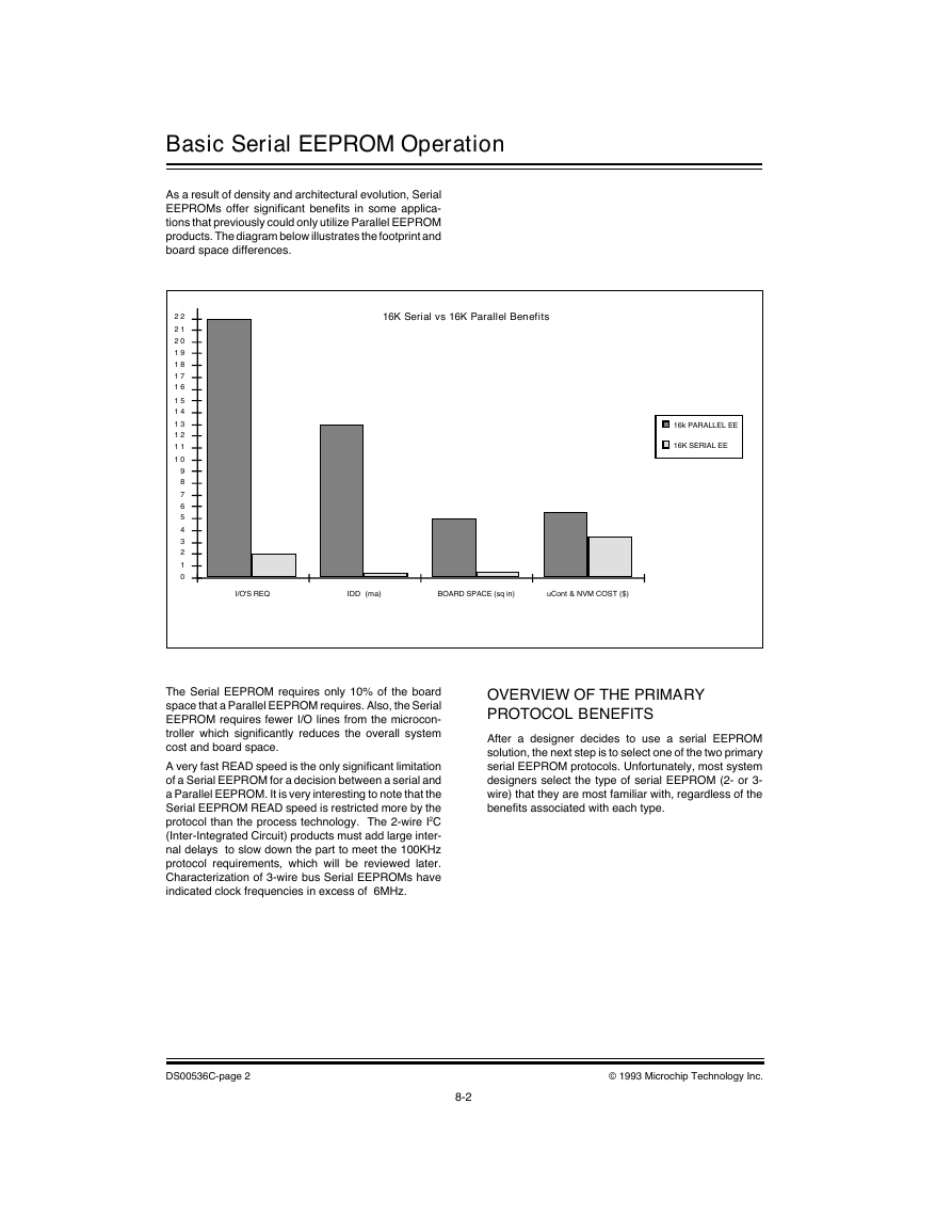
As a result of density and architectural evolution, Serial
EEPROMs offer significant benefits in some applica-
tions that previously could only utilize Parallel EEPROM
products. The diagram below illustrates the footprint and
board space differences.
16K Serial vs 16K Parallel Benefits
16k PARALLEL EE
16K SERIAL EE
2 3
2 2
2 1
2 0
1 9
1 8
1 7
1 6
1 5
1 4
1 3
1 2
1 1
1 0
9
8
7
6
5
4
3
2
1
0
I/O'S REQ
IDD (ma)
BOARD SPACE (sq in)
uCont & NVM COST ($)
The Serial EEPROM requires only 10% of the board
space that a Parallel EEPROM requires. Also, the Serial
EEPROM requires fewer I/O lines from the microcon-
troller which significantly reduces the overall system
cost and board space.
A very fast READ speed is the only significant limitation
of a Serial EEPROM for a decision between a serial and
a Parallel EEPROM. It is very interesting to note that the
Serial EEPROM READ speed is restricted more by the
protocol than the process technology. The 2-wire I2C
(Inter-Integrated Circuit) products must add large inter-
nal delays to slow down the part to meet the 100KHz
protocol requirements, which will be reviewed later.
Characterization of 3-wire bus Serial EEPROMs have
indicated clock frequencies in excess of 6MHz.
OVERVIEW OF THE PRIMARY
PROTOCOL BENEFITS
After a designer decides to use a serial EEPROM
solution, the next step is to select one of the two primary
serial EEPROM protocols. Unfortunately, most system
designers select the type of serial EEPROM (2- or 3-
wire) that they are most familiar with, regardless of the
benefits associated with each type.
DS00536C-page 2
© 1993 Microchip Technology Inc.
8-2
�
Basic Serial EEPROM Operation
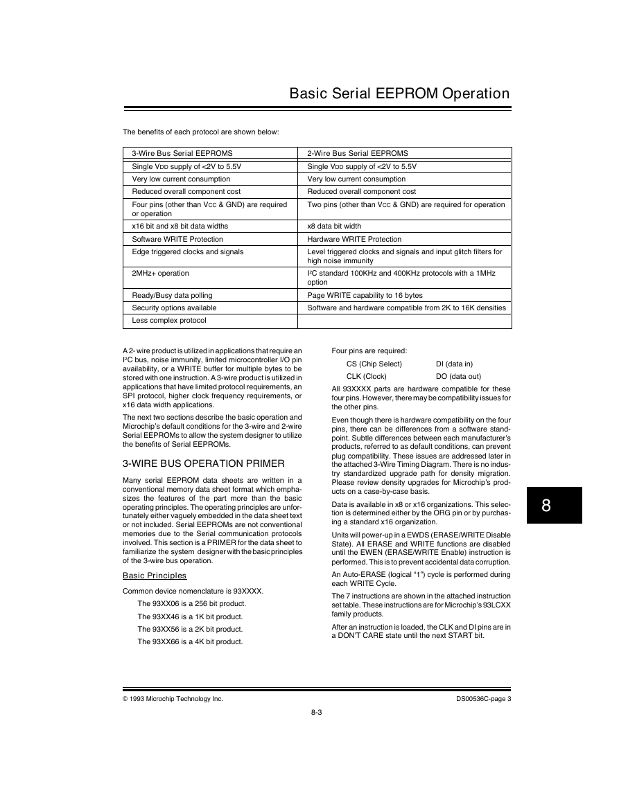
The benefits of each protocol are shown below:
3-Wire Bus Serial EEPROMS
Single VDD supply of <2V to 5.5V
Very low current consumption
Reduced overall component cost
Four pins (other than VCC & GND) are required
or operation
x16 bit and x8 bit data widths
Software WRITE Protection
Edge triggered clocks and signals
2MHz+ operation
Ready/Busy data polling
Security options available
Less complex protocol
A 2- wire product is utilized in applications that require an
I2C bus, noise immunity, limited microcontroller I/O pin
availability, or a WRITE buffer for multiple bytes to be
stored with one instruction. A 3-wire product is utilized in
applications that have limited protocol requirements, an
SPI protocol, higher clock frequency requirements, or
x16 data width applications.
The next two sections describe the basic operation and
Microchip’s default conditions for the 3-wire and 2-wire
Serial EEPROMs to allow the system designer to utilize
the benefits of Serial EEPROMs.
3-WIRE BUS OPERATION PRIMER
Many serial EEPROM data sheets are written in a
conventional memory data sheet format which empha-
sizes the features of the part more than the basic
operating principles. The operating principles are unfor-
tunately either vaguely embedded in the data sheet text
or not included. Serial EEPROMs are not conventional
memories due to the Serial communication protocols
involved. This section is a PRIMER for the data sheet to
familiarize the system designer with the basic principles
of the 3-wire bus operation.
Basic Principles
Common device nomenclature is 93XXXX.
The 93XX06 is a 256 bit product.
The 93XX46 is a 1K bit product.
The 93XX56 is a 2K bit product.
The 93XX66 is a 4K bit product.
2-Wire Bus Serial EEPROMS
Single VDD supply of <2V to 5.5V
Very low current consumption
Reduced overall component cost
Two pins (other than VCC & GND) are required for operation
x8 data bit width
Hardware WRITE Protection
Level triggered clocks and signals and input glitch filters for
high noise immunity
I2C standard 100KHz and 400KHz protocols with a 1MHz
option
Page WRITE capability to 16 bytes
Software and hardware compatible from 2K to 16K densities
Four pins are required:
CS (Chip Select)
CLK (Clock)
DI (data in)
DO (data out)
All 93XXXX parts are hardware compatible for these
four pins. However, there may be compatibility issues for
the other pins.
Even though there is hardware compatibility on the four
pins, there can be differences from a software stand-
point. Subtle differences between each manufacturer’s
products, referred to as default conditions, can prevent
plug compatibility. These issues are addressed later in
the attached 3-Wire Timing Diagram. There is no indus-
try standardized upgrade path for density migration.
Please review density upgrades for Microchip’s prod-
ucts on a case-by-case basis.
Data is available in x8 or x16 organizations. This selec-
tion is determined either by the ORG pin or by purchas-
ing a standard x16 organization.
Units will power-up in a EWDS (ERASE/WRITE Disable
State). All ERASE and WRITE functions are disabled
until the EWEN (ERASE/WRITE Enable) instruction is
performed. This is to prevent accidental data corruption.
An Auto-ERASE (logical “1”) cycle is performed during
each WRITE Cycle.
The 7 instructions are shown in the attached instruction
set table. These instructions are for Microchip’s 93LCXX
family products.
After an instruction is loaded, the CLK and DI pins are in
a DON’T CARE state until the next START bit.
8
© 1993 Microchip Technology Inc.
DS00536C-page 3
8-3
�
Basic Serial EEPROM Operation
The following is required for each instruction set (all
input bits are triggered by the positive clock edges):
Start Bit
The first Data-in high signal clocked in
after CS is high.
Two Bits to identify the instruction
Refer to the Instruction Set table for the
number of bits required.
Separate data-in and data-out pins. How-
ever, these two pins may be tied together
for true 3-wire operation. Please refer to
the attached 3-wire Bus READ timing
diagram example.
Opcode
Address
Data
READ, WRITE, and ERASE
The attached 93LC66 timing diagrams illustrate the key
concepts and timing parameters for each of these op-
erations. Please refer to the instruction set tables and
the AC parameters in the databook for supplemental
information.
ERASE ALL (ERAL)
An ERASE ALL (ERAL) operation is identified by a “00”
opcode. The ERAL instruction requires the next two bits
to be clocked in as “10” in the address block of the
instruction set. All bits in the array will be set to a logic
“1” state by one command in typically less than 10ms.
WRITE ALL (WRAL)
A WRITE ALL (WRAL) operation is also identified by a
“00” opcode. The WRAL requires the next two bits to be
clocked in as “01” in the address block of the instruction
set. The data-in block will contain the data for a SINGLE
BYTE which is to be repeated throughout the entire
array. For example, if a 4F5A is loaded in the 16 data-in
bits of the instruction set, a 4F5A will be written into every
word in the array.
EWEN and EWDS
As stated before, all units will power up in to an ERASE/
WRITE DISABLE (EWDS) state to prevent data corrup-
tion. All future ERASE/WRITE operations must execute
an ERASE/WRITE ENABLE (EWEN) opcode until the
next power down is detected or until other EWDS
opcodes are executed. Please refer to the instruction set
table.
DS00536C-page 4
© 1993 Microchip Technology Inc.
8-4
�
Basic Serial EEPROM Operation
INSTRUCTION SET FOR 93LC46: ORG = 1 (x 16 organization)
Instruction
READ
EWEN
ERASE
ERAL
WRITE
WRAL
EWDS
SB
1
1
1
1
1
1
1
Opcode
Address
Data In
10
00
11
00
01
00
00
A5 A4 A3 A2 A1 A0
1 1 X X X X
A5 A4 A3 A2 A1 A0
1 0 X X X X
A5 A4 A3 A2 A1 A0
0 1 X X X X
0 0 X X X X
—
—
—
—
D15 - D0
D15 - D0
—
INSTRUCTION SET FOR 93LC46: ORG = 0 (x 8 organization)
Instruction
READ
EWEN
ERASE
ERAL
WRITE
WRAL
EWDS
SB
1
1
1
1
1
1
1
Opcode
Address
Data In
10
00
11
00
01
00
00
A6 A5 A4 A3 A2 A1 A0
1 1 X X X X X
A6 A5 A4 A3 A2 A1 A0
1 0 X X X X X
A6 A5 A4 A3 A2 A1 A0
0 1 X X X X X
0 0 X X X X X
—
—
—
—
D7 - D0
D7 - D0
—
INSTRUCTION SET FOR 93LC56: ORG = 1 (x 16 organization)
Instruction
READ
EWEN
ERASE
ERAL
WRITE
WRAL
EWDS
SB
1
1
1
1
1
1
1
Opcode
Address
Data In
10
00
11
00
01
00
00
X A6 A5 A4 A3 A2 A1 A0
1 1 X X X X X X
X A6 A5 A4 A3 A2 A1 A0
1 0 X X X X X X
X A6 A5 A4 A3 A2 A1 A0
0 1 X X X X X X
0 0 X X X X X X
—
—
—
—
D15 - D0
D15 - D0
—
INSTRUCTION SET FOR 93LC56: ORG = 0 (x 8 organization)
Instruction
READ
EWEN
ERASE
ERAL
WRITE
WRAL
EWDS
SB
1
1
1
1
1
1
1
Opcode
Address
Data In
10
00
11
00
01
00
00
X A7 A6 A5 A4 A3 A2 A1 A0
1 1 X X X X X X X
X A7 A6 A5 A4 A3 A2 A1 A0
1 0 X X X X X X X
X A7 A6 A5 A4 A3 A2 A1 A0
0 1 X X X X X X X
0 0 X X X X X X X
—
—
—
—
D7 - D0
D7 - D0
—
INSTRUCTION SET FOR 93LC66: ORG = 1 (x 16 organization)
Instruction
READ
EWEN
ERASE
ERAL
WRITE
WRAL
EWDS
SB
1
1
1
1
1
1
1
Opcode
10
00
11
00
01
00
00
Address
A7 - A0
11XXXXXX
A7 - A0
10XXXXXX
A7 - A0
01XXXXXX
00XXXXXX
Data In
—
—
—
—
D15 - D0
D15 - D0
—
INSTRUCTION SET FOR 93LC66: ORG = 0 (x 8 organization)
Data In
Opcode
Instruction
READ
EWEN
ERASE
ERAL
WRITE
WRAL
EWDS
SB
1
1
1
1
1
1
1
10
00
11
00
01
00
00
Address
A8 - A0
11XXXXXXX
A8 - A0
10XXXXXXX
A8 - A0
01XXXXXXX
00XXXXXXX
—
—
—
—
D7 - D0
D7 - D0
—
Data Out
D15 - D0
High-Z
(RDY/BSY)
(RDY/BSY)
(RDY/BSY)
(RDY/BSY)
High-Z
Data Out
D7 - D0
High-Z
(RDY/BSY)
(RDY/BSY)
(RDY/BSY)
(RDY/BSY)
High-Z
Data Out
D15 - D0
High-Z
(RDY/BSY)
(RDY/BSY)
(RDY/BSY)
(RDY/BSY)
High-Z
Data Out
D7 - D0
High-Z
(RDY/BSY)
(RDY/BSY)
(RDY/BSY)
(RDY/BSY)
High-Z
Req. CLK Cycles
25
9
9
9
25
25
9
Req. CLK Cycles
18
10
10
10
18
18
10
Req. CLK Cycles
27
11
11
11
27
27
11
Req. CLK Cycles
20
12
12
12
20
20
12
Data Out
D15 - D0
High-Z
(RDY/BSY)
(RDY/BSY)
(RDY/BSY)
(RDY/BSY)
High-Z
Data Out
D7 - D0
High-Z
(RDY/BSY)
(RDY/BSY)
(RDY/BSY)
(RDY/BSY)
High-Z
Req. CLK Cycles
8
27
11
11
11
27
27
11
Req. CLK Cycles
20
12
12
12
20
20
12
© 1993 Microchip Technology Inc.
DS00536C-page 5
8-5
�
Basic Serial EEPROM Operation
Data is recognized as valid while SCL is high. The data
on SDA must observe data in set-up and hold specifica-
tions before and after SCL is pulsed. There is only one
bit of data for each SCL pulse.
Control Byte Requirements
After a START bit, each command begins with an 8 bit
control byte sent by the master. This control byte has the
following three primary functions before the data and/or
word address information is loaded for all commands:
Identify the serial EEPROM as the slave addressed on
the bus.
Select the specific serial EEPROM or the internal memory
block on the bus. There may be up to 8 serial EEPROMs
on the bus)
Select the READ or WRITE function for the next com-
mand transmitted by the master.
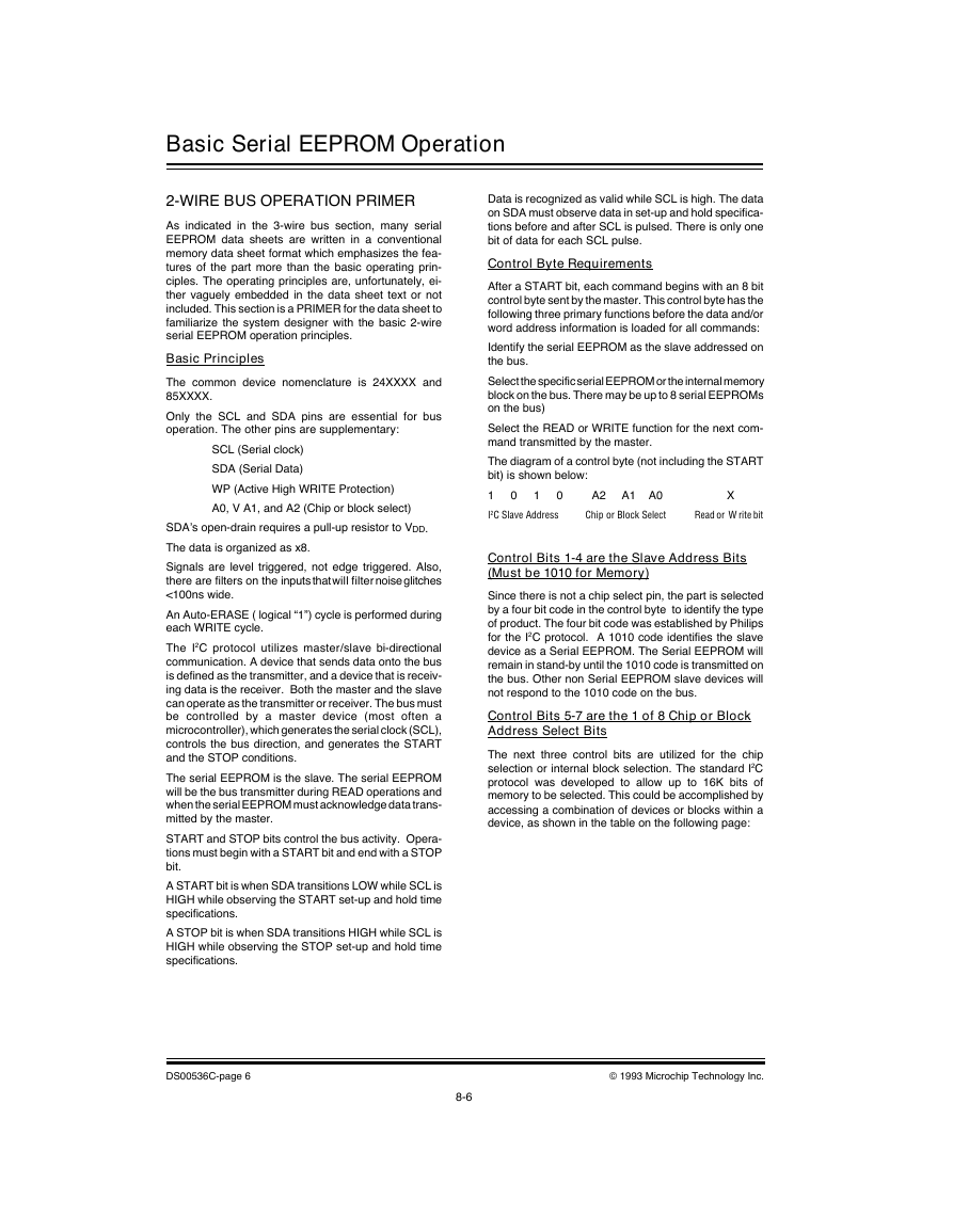
The diagram of a control byte (not including the START
bit) is shown below:
0
1
I2C Slave Address
A2 A1 A0
Chip or Block Select
Read or W rite bit
0
1
X
Control Bits 1-4 are the Slave Address Bits
(Must be 1010 for Memory)
Since there is not a chip select pin, the part is selected
by a four bit code in the control byte to identify the type
of product. The four bit code was established by Philips
for the I2C protocol. A 1010 code identifies the slave
device as a Serial EEPROM. The Serial EEPROM will
remain in stand-by until the 1010 code is transmitted on
the bus. Other non Serial EEPROM slave devices will
not respond to the 1010 code on the bus.
Control Bits 5-7 are the 1 of 8 Chip or Block
Address Select Bits
The next three control bits are utilized for the chip
selection or internal block selection. The standard I2C
protocol was developed to allow up to 16K bits of
memory to be selected. This could be accomplished by
accessing a combination of devices or blocks within a
device, as shown in the table on the following page:
2-WIRE BUS OPERATION PRIMER
As indicated in the 3-wire bus section, many serial
EEPROM data sheets are written in a conventional
memory data sheet format which emphasizes the fea-
tures of the part more than the basic operating prin-
ciples. The operating principles are, unfortunately, ei-
ther vaguely embedded in the data sheet text or not
included. This section is a PRIMER for the data sheet to
familiarize the system designer with the basic 2-wire
serial EEPROM operation principles.
Basic Principles
The common device nomenclature is 24XXXX and
85XXXX.
Only the SCL and SDA pins are essential for bus
operation. The other pins are supplementary:
SCL (Serial clock)
SDA (Serial Data)
WP (Active High WRITE Protection)
A0, V A1, and A2 (Chip or block select)
SDA’s open-drain requires a pull-up resistor to VDD.
The data is organized as x8.
Signals are level triggered, not edge triggered. Also,
there are filters on the inputs that will filter noise glitches
<100ns wide.
An Auto-ERASE ( logical “1”) cycle is performed during
each WRITE cycle.
The I2C protocol utilizes master/slave bi-directional
communication. A device that sends data onto the bus
is defined as the transmitter, and a device that is receiv-
ing data is the receiver. Both the master and the slave
can operate as the transmitter or receiver. The bus must
be controlled by a master device (most often a
microcontroller), which generates the serial clock (SCL),
controls the bus direction, and generates the START
and the STOP conditions.
The serial EEPROM is the slave. The serial EEPROM
will be the bus transmitter during READ operations and
when the serial EEPROM must acknowledge data trans-
mitted by the master.
START and STOP bits control the bus activity. Opera-
tions must begin with a START bit and end with a STOP
bit.
A START bit is when SDA transitions LOW while SCL is
HIGH while observing the START set-up and hold time
specifications.
A STOP bit is when SDA transitions HIGH while SCL is
HIGH while observing the STOP set-up and hold time
specifications.
DS00536C-page 6
© 1993 Microchip Technology Inc.
8-6
�
Basic Serial EEPROM Operation
Device
24LC01B, 24C01,85C72
24LC02B, 24C02,85C82
24LC04B, 24C04,85C92
24LC08B
24LC16B
K bits
Density
Internal
Blocks
1
2
4
8
16
1
1
2
4
8
A0
H or L
H or L
X
X
X
A1
H or L
H or L
H or L
X
X
A2
H or L
H or L
H or L
H or L
X
Bus Access Devices
Up to 8 devices
Up to 8 devices
Up to 4 devices
Up to 2 devices
Only 1 device
X= NOT USED. This pin must be tied to VSS or VDD. It is not recommended to FLOAT these pins since there may be test
modes accessed to these pins via a high voltage signal.
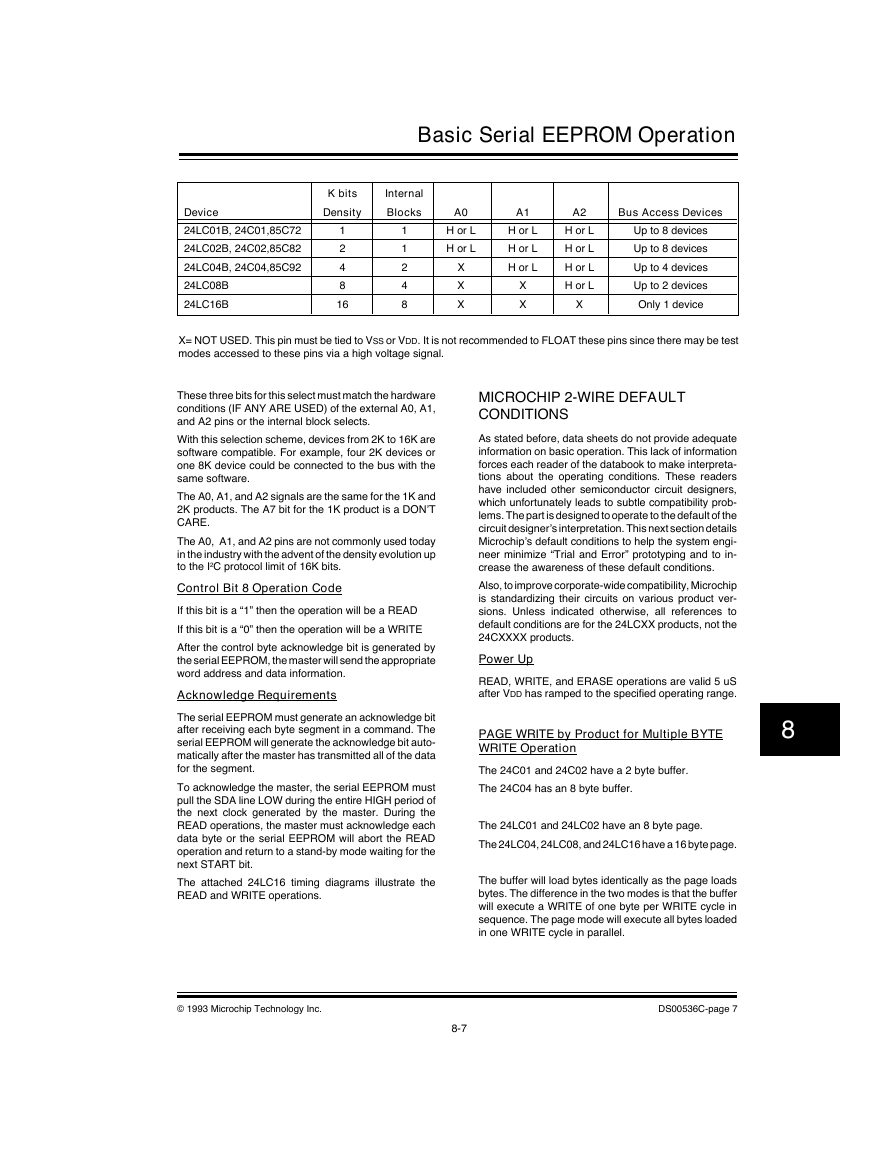
These three bits for this select must match the hardware
conditions (IF ANY ARE USED) of the external A0, A1,
and A2 pins or the internal block selects.
With this selection scheme, devices from 2K to 16K are
software compatible. For example, four 2K devices or
one 8K device could be connected to the bus with the
same software.
The A0, A1, and A2 signals are the same for the 1K and
2K products. The A7 bit for the 1K product is a DON’T
CARE.
The A0, A1, and A2 pins are not commonly used today
in the industry with the advent of the density evolution up
to the I2C protocol limit of 16K bits.
Control Bit 8 Operation Code
If this bit is a “1” then the operation will be a READ
If this bit is a “0” then the operation will be a WRITE
After the control byte acknowledge bit is generated by
the serial EEPROM, the master will send the appropriate
word address and data information.
Acknowledge Requirements
The serial EEPROM must generate an acknowledge bit
after receiving each byte segment in a command. The
serial EEPROM will generate the acknowledge bit auto-
matically after the master has transmitted all of the data
for the segment.
To acknowledge the master, the serial EEPROM must
pull the SDA line LOW during the entire HIGH period of
the next clock generated by the master. During the
READ operations, the master must acknowledge each
data byte or the serial EEPROM will abort the READ
operation and return to a stand-by mode waiting for the
next START bit.
The attached 24LC16 timing diagrams illustrate the
READ and WRITE operations.
MICROCHIP 2-WIRE DEFAULT
CONDITIONS
As stated before, data sheets do not provide adequate
information on basic operation. This lack of information
forces each reader of the databook to make interpreta-
tions about the operating conditions. These readers
have included other semiconductor circuit designers,
which unfortunately leads to subtle compatibility prob-
lems. The part is designed to operate to the default of the
circuit designer’s interpretation. This next section details
Microchip’s default conditions to help the system engi-
neer minimize “Trial and Error” prototyping and to in-
crease the awareness of these default conditions.
Also, to improve corporate-wide compatibility, Microchip
is standardizing their circuits on various product ver-
sions. Unless indicated otherwise, all references to
default conditions are for the 24LCXX products, not the
24CXXXX products.
Power Up
READ, WRITE, and ERASE operations are valid 5 uS
after VDD has ramped to the specified operating range.
PAGE WRITE by Product for Multiple BYTE
WRITE Operation
The 24C01 and 24C02 have a 2 byte buffer.
The 24C04 has an 8 byte buffer.
The 24LC01 and 24LC02 have an 8 byte page.
The 24LC04, 24LC08, and 24LC16 have a 16 byte page.
The buffer will load bytes identically as the page loads
bytes. The difference in the two modes is that the buffer
will execute a WRITE of one byte per WRITE cycle in
sequence. The page mode will execute all bytes loaded
in one WRITE cycle in parallel.
8
© 1993 Microchip Technology Inc.
DS00536C-page 7
8-7
�
Basic Serial EEPROM Operation
There are pages within blocks. For a 16 byte page
product, the most significant 4 bits of the word address
point to the page address and the least significant 4 bits
point to the byte address within a page. For an 8 byte
page product, the most significant 5 bits of the word
address point to the page address and the least signifi-
cant 3 bits point to the byte address within a page.
The number of bytes loaded in to the page is from one
byte up to the page size. For example, three bytes can
be loaded into the 16 byte page of the 24LC16. If during
the loading of the fourth byte a STOP bit is received, the
page will WRITE three bytes. The fourth byte will not be
written since loading the fourth byte was not complete.
NOTE: New versions released in March 1993 will
default to ABORTING the entire operation if a
STOP bit is received in the middle of a byte
while loading a page.
If more than 16 bytes are loaded in the page of a 16 byte
page product, then the 17th byte will override the data
loaded into the original first byte (the page data will wrap
around WITHIN a page). Therefore, the system de-
signer must take precautions to not WRITE over a page
boundary during a multiple byte WRITE operation.
Bytes not changed in the page will NOT result in data
corruption in the array. For example, If two bytes are
loaded in to the 24LC16 page with the least significant
word address bits of 0000 and then a STOP bit is
transmitted. Bytes 1 and 2 in the array will have the data
changed to the new page contents. Bytes 3 through 16
WILL NOT change.
The WRITE operation will not be executed until a STOP
bit is transmitted.
At this point, the serial EEPROM is free from the bus
since the actual WRITE function is self-timed. There-
fore, the microcontroller interfacing to the serial EEPROM
may perform other functions not associated to commu-
nication with the serial EEPROM during the self-timed
WRITE operations.
Once the part is in the auto-ERASE mode, it will com-
plete the ERASE/WRITE operation unless power is
removed. STOP and START bits will be ignored.
READ
Once the Serial EEPROM is in a RANDOM READ
operation, it can be placed into the sequential READ
operation. If the master issues an acknowledge bit
instead of a STOP bit, the Serial EEPROM will READ the
next sequential 8 bits. The Serial will wait for the next bit
command from the master. The sequential READ will
continue as long as the master issues an acknowledge
bit on the next clock cycle after the last bit is READ. The
READ will continue from block to block and will wrap
around if the last bit in the array is addressed. Again, this
will continue until the master issues a STOP bit instead
of an acknowledge bit.
While reading zeroes the master cannot pull SDA high
to generate a STOP bit, since the serial EEPROM SDA
pin is outputting a low. To recover from a fault during a
READ, repeat 9 clocks with data floating high. There-
fore, the acknowledge bit will not occur and the part will
reset and return to stand-by.
A START bit during an operation will cease the current
operation and begin the next operation.
Author:
Steve Drehobl
Memory Products Division
DS00536C-page 8
© 1993 Microchip Technology Inc.
8-8
�





 2023年江西萍乡中考道德与法治真题及答案.doc
 2012年重庆南川中考生物真题及答案.doc
 2013年江西师范大学地理学综合及文艺理论基础考研真题.doc
 2020年四川甘孜小升初语文真题及答案I卷.doc
 2020年注册岩土工程师专业基础考试真题及答案.doc
 2023-2024学年福建省厦门市九年级上学期数学月考试题及答案.doc
 2021-2022学年辽宁省沈阳市大东区九年级上学期语文期末试题及答案.doc
 2022-2023学年北京东城区初三第一学期物理期末试卷及答案.doc
 2018上半年江西教师资格初中地理学科知识与教学能力真题及答案.doc
 2012年河北国家公务员申论考试真题及答案-省级.doc
 2020-2021学年江苏省扬州市江都区邵樊片九年级上学期数学第一次质量检测试题及答案.doc
 2022下半年黑龙江教师资格证中学综合素质真题及答案.doc