Downloaded from SAE International by Tsinghua University, Sunday, April 07, 2019
SURFACE VEHICLE
INFORMATION REPORT
J2716™
APR2016
Issued
Revised
Superseding J2716 JAN2010
2007-04
2016-04
(R) SENT - Single Edge Nibble Transmission for Automotive Applications
RATIONALE
1. Clarified clock variation refers to variation in clock tick time.
2. New appendix for High Speed 12 bit Sensors.
3. Changes for initialization and non-usage of serial message.
4. Changes to support option for independent 5V supply in sensor
5. Serial message cycle changed to ≤ 64 messages for greater flexibility and to allow more time for diagnostic
information.
6. Clarification to EMC Susceptibility testing guidelines for Erroneous SENT frames which remain undetected by the
SENT CRC
7. Added Appendix A.6 Temperature Sensor requirements
8. Added APPENDIX E
9. Added APPENDIX G for recommended connector
10. Created APPENDIX H (SENT Data Frame Formats) and moved generic sensor requirements from APPENDIX A
to APPENDIX H
11. Changes to support higher current sensors
12. Added E.3 Error Messages and Signals
13. Added A.7 Position Sensors and Combined Position Temperature Sensors
14. Added Overview of SENT standard structure (3.2)
__________________________________________________________________________________________________________________________________________
SAE Technical Standards Board Rules provide that: “This report is published by SAE to advance the state of technical and engineering sciences. The use of this report is entirely
voluntary, and its applicability and suitability for any particular use, including any patent infringement arising therefrom, is the sole responsibility of the user.”
SAE reviews each technical report at least every five years at which time it may be revised, reaffirmed, stabilized, or cancelled. SAE invites your written comments and
suggestions.
Copyright © 2015 SAE International
All rights reserved. No part of this publication may be reproduced, stored in a retrieval system or transmitted, in any form or by any means, electronic, mechanical, photocopying,
recording, or otherwise, without the prior written permission of SAE.
TO PLACE A DOCUMENT ORDER:
SAE WEB ADDRESS:
Tel: 877-606-7323 (inside USA and Canada)
Tel: +1 724-776-4970 (outside USA)
Fax: 724-776-0790
Email: CustomerService@sae.org
http://www.sae.org
SAE values your input. To provide feedback
on this Technical Report, please visit
http://www.sae.org/technical/standards/J2716_201604
�
SAE INTERNATIONAL
Downloaded from SAE International by Tsinghua University, Sunday, April 07, 2019
J2716™ APR2016
Page 2 of 120
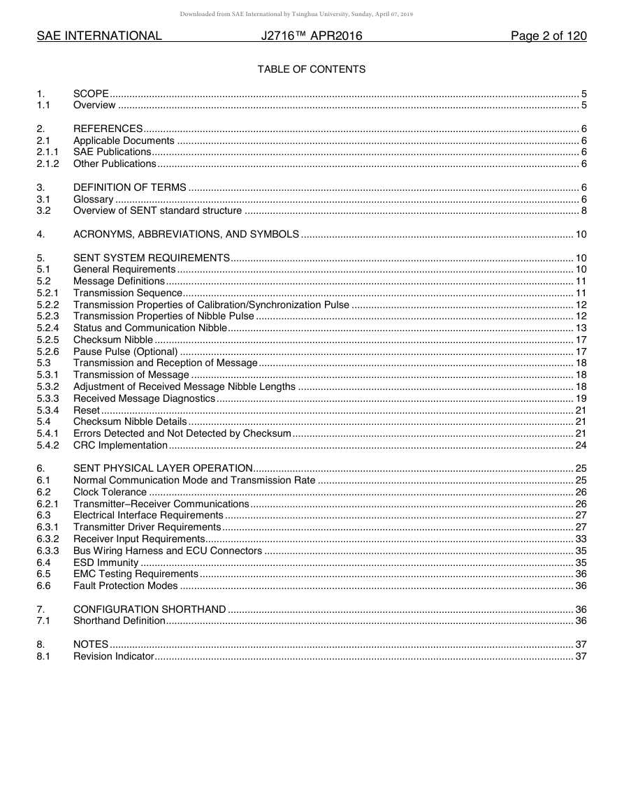
TABLE OF CONTENTS
ACRONYMS, ABBREVIATIONS, AND SYMBOLS ................................................................................................. 10
SCOPE ....................................................................................................................................................................... 5
Overview .................................................................................................................................................................... 5
DEFINITION OF TERMS ........................................................................................................................................... 6
Glossary ..................................................................................................................................................................... 6
Overview of SENT standard structure ....................................................................................................................... 8
1.
1.1
REFERENCES ........................................................................................................................................................... 6
2.
2.1
Applicable Documents ............................................................................................................................................... 6
2.1.1 SAE Publications ........................................................................................................................................................ 6
2.1.2 Other Publications ...................................................................................................................................................... 6
3.
3.1
3.2
4.
SENT SYSTEM REQUIREMENTS .......................................................................................................................... 10
5.
General Requirements ............................................................................................................................................. 10
5.1
Message Definitions ................................................................................................................................................. 11
5.2
5.2.1 Transmission Sequence ........................................................................................................................................... 11
5.2.2 Transmission Properties of Calibration/Synchronization Pulse ............................................................................... 12
5.2.3 Transmission Properties of Nibble Pulse ................................................................................................................. 12
5.2.4 Status and Communication Nibble ........................................................................................................................... 13
5.2.5 Checksum Nibble ..................................................................................................................................................... 17
5.2.6 Pause Pulse (Optional) ............................................................................................................................................ 17
5.3
Transmission and Reception of Message ................................................................................................................ 18
5.3.1 Transmission of Message ........................................................................................................................................ 18
5.3.2 Adjustment of Received Message Nibble Lengths .................................................................................................. 18
5.3.3 Received Message Diagnostics ............................................................................................................................... 19
5.3.4 Reset ........................................................................................................................................................................ 21
5.4
Checksum Nibble Details ......................................................................................................................................... 21
5.4.1 Errors Detected and Not Detected by Checksum .................................................................................................... 21
5.4.2 CRC Implementation ................................................................................................................................................ 24
6.
SENT PHYSICAL LAYER OPERATION .................................................................................................................. 25
6.1
Normal Communication Mode and Transmission Rate ........................................................................................... 25
6.2
Clock Tolerance ....................................................................................................................................................... 26
6.2.1 Transmitter–Receiver Communications ................................................................................................................... 26
6.3
Electrical Interface Requirements ............................................................................................................................ 27
6.3.1 Transmitter Driver Requirements ............................................................................................................................. 27
6.3.2 Receiver Input Requirements................................................................................................................................... 33
6.3.3 Bus Wiring Harness and ECU Connectors .............................................................................................................. 35
ESD Immunity .......................................................................................................................................................... 35
6.4
EMC Testing Requirements ..................................................................................................................................... 36
6.5
6.6
Fault Protection Modes ............................................................................................................................................ 36
7.
7.1
8.
8.1
CONFIGURATION SHORTHAND ........................................................................................................................... 36
Shorthand Definition ................................................................................................................................................. 36
NOTES ..................................................................................................................................................................... 37
Revision Indicator ..................................................................................................................................................... 37
�
Downloaded from SAE International by Tsinghua University, Sunday, April 07, 2019
J2716™ APR2016
Page 3 of 120
Recommended application specific protocols ...................................................................................... 38
Checksum examples ............................................................................................................................ 51
Testing guidelines ................................................................................................................................. 55
Serial channel message IDS ................................................................................................................ 58
Common sensor definitions .................................................................................................................. 76
Fast channel multiplexing ..................................................................................................................... 93
SENT connectors ............................................................................................................................... 101
SENT data frame formats ................................................................................................................... 103
Alternative receiver circuit .................................................................................................................. 118
SAE INTERNATIONAL
Appendix A
Appendix B
Appendix C
Appendix D
Appendix E
Appendix F
Appendix G
Appendix H
Appendix I
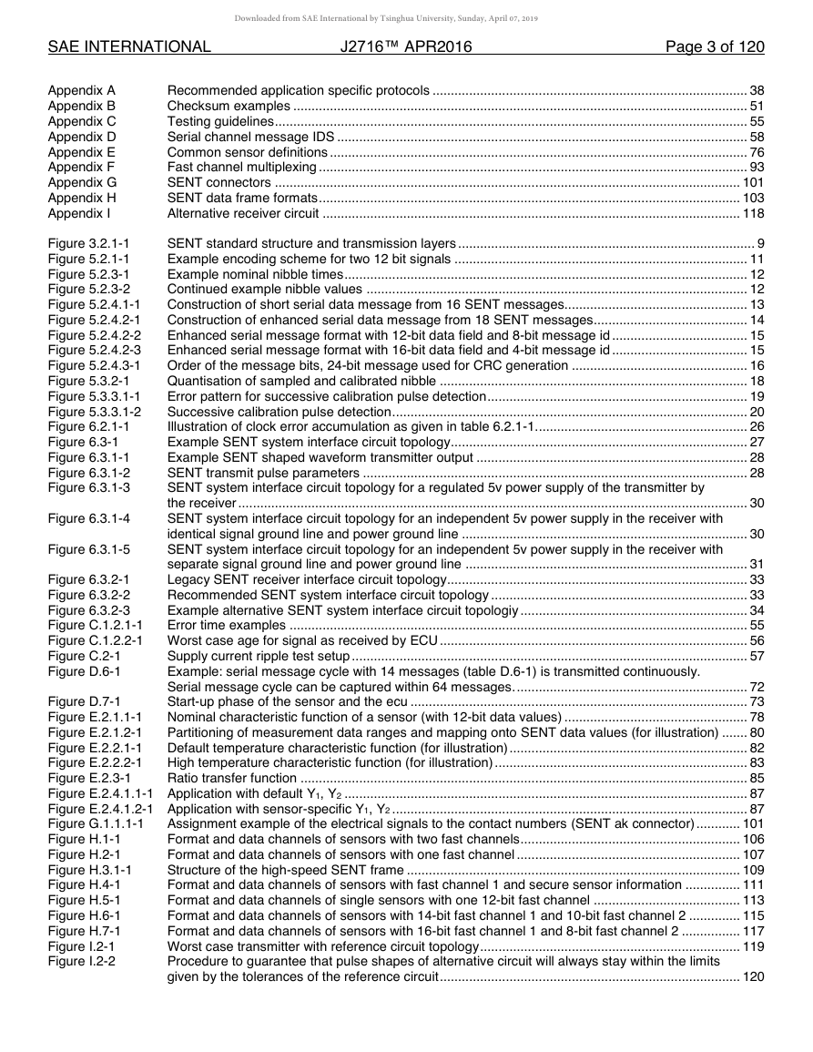
Figure 3.2.1-1
Figure 5.2.1-1
Figure 5.2.3-1
Figure 5.2.3-2
Figure 5.2.4.1-1
Figure 5.2.4.2-1
Figure 5.2.4.2-2
Figure 5.2.4.2-3
Figure 5.2.4.3-1
Figure 5.3.2-1
Figure 5.3.3.1-1
Figure 5.3.3.1-2
Figure 6.2.1-1
Figure 6.3-1
Figure 6.3.1-1
Figure 6.3.1-2
Figure 6.3.1-3
Figure 6.3.1-5
Figure 6.3.1-4
SENT standard structure and transmission layers ................................................................................. 9
Example encoding scheme for two 12 bit signals ................................................................................ 11
Example nominal nibble times .............................................................................................................. 12
Continued example nibble values ........................................................................................................ 12
Construction of short serial data message from 16 SENT messages.................................................. 13
Construction of enhanced serial data message from 18 SENT messages .......................................... 14
Enhanced serial message format with 12-bit data field and 8-bit message id ..................................... 15
Enhanced serial message format with 16-bit data field and 4-bit message id ..................................... 15
Order of the message bits, 24-bit message used for CRC generation ................................................ 16
Quantisation of sampled and calibrated nibble .................................................................................... 18
Error pattern for successive calibration pulse detection ....................................................................... 19
Successive calibration pulse detection ................................................................................................. 20
Illustration of clock error accumulation as given in table 6.2.1-1. ......................................................... 26
Example SENT system interface circuit topology ................................................................................. 27
Example SENT shaped waveform transmitter output .......................................................................... 28
SENT transmit pulse parameters ......................................................................................................... 28
SENT system interface circuit topology for a regulated 5v power supply of the transmitter by
the receiver ........................................................................................................................................... 30
SENT system interface circuit topology for an independent 5v power supply in the receiver with
identical signal ground line and power ground line .............................................................................. 30
SENT system interface circuit topology for an independent 5v power supply in the receiver with
separate signal ground line and power ground line ............................................................................. 31
Legacy SENT receiver interface circuit topology.................................................................................. 33
Figure 6.3.2-1
Recommended SENT system interface circuit topology ...................................................................... 33
Figure 6.3.2-2
Example alternative SENT system interface circuit topologiy .............................................................. 34
Figure 6.3.2-3
Error time examples ............................................................................................................................. 55
Figure C.1.2.1-1
Figure C.1.2.2-1 Worst case age for signal as received by ECU .................................................................................... 56
Supply current ripple test setup ............................................................................................................ 57
Figure C.2-1
Example: serial message cycle with 14 messages (table D.6-1) is transmitted continuously.
Figure D.6-1
Serial message cycle can be captured within 64 messages. ............................................................... 72
Start-up phase of the sensor and the ecu ............................................................................................ 73
Figure D.7-1
Nominal characteristic function of a sensor (with 12-bit data values) .................................................. 78
Figure E.2.1.1-1
Partitioning of measurement data ranges and mapping onto SENT data values (for illustration) ....... 80
Figure E.2.1.2-1
Default temperature characteristic function (for illustration) ................................................................. 82
Figure E.2.2.1-1
High temperature characteristic function (for illustration) ..................................................................... 83
Figure E.2.2.2-1
Ratio transfer function .......................................................................................................................... 85
Figure E.2.3-1
Figure E.2.4.1.1-1 Application with default Y1, Y2 .............................................................................................................. 87
Figure E.2.4.1.2-1 Application with sensor-specific Y1, Y2 ................................................................................................. 87
Assignment example of the electrical signals to the contact numbers (SENT ak connector) ............ 101
Figure G.1.1.1-1
Format and data channels of sensors with two fast channels ............................................................ 106
Figure H.1-1
Format and data channels of sensors with one fast channel ............................................................. 107
Figure H.2-1
Structure of the high-speed SENT frame ........................................................................................... 109
Figure H.3.1-1
Format and data channels of sensors with fast channel 1 and secure sensor information ............... 111
Figure H.4-1
Format and data channels of single sensors with one 12-bit fast channel ........................................ 113
Figure H.5-1
Format and data channels of sensors with 14-bit fast channel 1 and 10-bit fast channel 2 .............. 115
Figure H.6-1
Format and data channels of sensors with 16-bit fast channel 1 and 8-bit fast channel 2 ................ 117
Figure H.7-1
Worst case transmitter with reference circuit topology ....................................................................... 119
Figure I.2-1
Procedure to guarantee that pulse shapes of alternative circuit will always stay within the limits
Figure I.2-2
given by the tolerances of the reference circuit .................................................................................. 120
�
SAE INTERNATIONAL
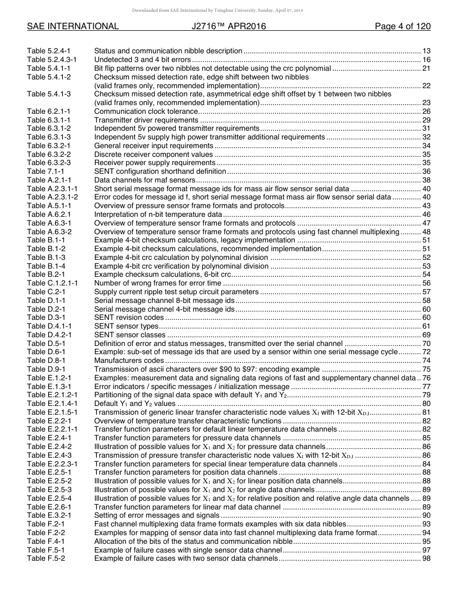
Table 5.2.4-1
Table 5.2.4.3-1
Table 5.4.1-1
Table 5.4.1-2
Table 5.4.1-3
Table 6.2.1-1
Table 6.3.1-1
Table 6.3.1-2
Table 6.3.1-3
Table 6.3.2-1
Table 6.3.2-2
Table 6.3.2-3
Table 7.1-1
Table A.2.1-1
Table A.2.3.1-1
Table A.2.3.1-2
Table A.5.1-1
Table A.6.2.1
Table A.6.3-1
Table A.6.3-2
Table B.1-1
Table B.1-2
Table B.1-3
Table B.1-4
Table B.2-1
Table C.1.2.1-1
Table C.2-1
Table D.1-1
Table D.2-1
Table D.3-1
Table D.4.1-1
Table D.4.2-1
Table D.5-1
Table D.6-1
Table D.8-1
Table D.9-1
Table E.1.2-1
Table E.1.3-1
Table E.2.1.2-1
Table E.2.1.4-1
Table E.2.1.5-1
Table E.2.2-1
Table E.2.2.1-1
Table E.2.4-1
Table E.2.4-2
Table E.2.4-3
Table E.2.2.3-1
Table E.2.5-1
Table E.2.5-2
Table E.2.5-3
Table E.2.5-4
Table E.2.6-1
Table E.3.2-1
Table F.2-1
Table F.2-2
Table F.4-1
Table F.5-1
Table F.5-2
Downloaded from SAE International by Tsinghua University, Sunday, April 07, 2019
J2716™ APR2016
Page 4 of 120
Status and communication nibble description ...................................................................................... 13
Undetected 3 and 4 bit errors ............................................................................................................... 16
Bit flip patterns over two nibbles not detectable using the crc polynomial ........................................... 21
Checksum missed detection rate, edge shift between two nibbles
(valid frames only, recommended implementation).............................................................................. 22
Checksum missed detection rate, asymmetrical edge shift offset by 1 between two nibbles
(valid frames only, recommended implementation).............................................................................. 23
Communication clock tolerance............................................................................................................ 26
Transmitter driver requirements ........................................................................................................... 29
Independent 5v powered transmitter requirements .............................................................................. 31
Independent 5v supply high power transmitter additional requirements .............................................. 32
General receiver input requirements .................................................................................................... 34
Discrete receiver component values .................................................................................................... 35
Receiver power supply requirements ................................................................................................... 35
SENT configuration shorthand definition .............................................................................................. 36
Data channels for maf sensors ............................................................................................................. 38
Short serial message format message ids for mass air flow sensor serial data .................................. 40
Error codes for message id f, short serial message format mass air flow sensor serial data .............. 40
Overview of pressure sensor frame formats and protocols .................................................................. 43
Interpretation of n-bit temperature data ................................................................................................ 46
Overview of temperature sensor frame formats and protocols ............................................................ 47
Overview of temperature sensor frame formats and protocols using fast channel multiplexing .......... 48
Example 4-bit checksum calculations, legacy implementation ............................................................ 51
Example 4-bit checksum calculations, recommended implementation ................................................ 51
Example 4-bit crc calculation by polynominal division ......................................................................... 52
Example 4-bit crc verification by polynominal division ......................................................................... 53
Example checksum calculations, 6-bit crc ............................................................................................ 54
Number of wrong frames for error time ................................................................................................ 56
Supply current ripple test setup circuit parameters .............................................................................. 57
Serial message channel 8-bit message ids .......................................................................................... 58
Serial message channel 4-bit message ids .......................................................................................... 60
SENT revision codes ............................................................................................................................ 60
SENT sensor types ............................................................................................................................... 61
SENT sensor classes ........................................................................................................................... 69
Definition of error and status messages, transmitted over the serial channel ..................................... 70
Example: sub-set of message ids that are used by a sensor within one serial message cycle ........... 72
Manufacturers codes ............................................................................................................................ 74
Transmission of ascii characters over $90 to $97: encoding example ................................................ 75
Examples: measurement data and signaling data regions of fast and supplementary channel data .. 76
Error indicators / specific messages / initialization message ............................................................... 77
Partitioning of the signal data space with default Y1 and Y2 ................................................................. 79
Default Y1 and Y2 values ...................................................................................................................... 80
Transmission of generic linear transfer characteristic node values XI with 12-bit XD,I ......................... 81
Overview of temperature transfer characteristic functions ................................................................... 82
Transfer function parameters for default linear temperature data channels ........................................ 82
Transfer function parameters for pressure data channels ................................................................... 85
Illustration of possible values for X1 and X2 for pressure data channels .............................................. 86
Transmission of pressure transfer characteristic node values XI with 12-bit XD,I ................................ 86
Transfer function parameters for special linear temperature data channels ........................................ 84
Transfer function parameters for position data channels ..................................................................... 88
Illustration of possible values for X1 and X2 for linear position data channels...................................... 88
Illustration of possible values for X1 and X2 for angle data channels ................................................... 89
Illustration of possible values for X1 and X2 for relative position and relative angle data channels ..... 89
Transfer function parameters for linear maf data channel ................................................................... 89
Setting of error messages and signals ................................................................................................. 90
Fast channel multiplexing data frame formats examples with six data nibbles .................................... 93
Examples for mapping of sensor data into fast channel multiplexing data frame format ..................... 94
Allocation of the bits of the status and communication nibble .............................................................. 95
Example of failure cases with single sensor data channel ................................................................... 97
Example of failure cases with two sensor data channels ..................................................................... 98
�
SAE INTERNATIONAL
Table F.6.1-1
Table F.6.2-1
Table F.6.3-1
Table F.6.4-1
Table G.1.1.1-1
Table H-1
Table H-2
Table H.1-1
Table H.3.1-1
Table H.5-1
Table H.6-1
Table H.7-1
Table I.1-1
Downloaded from SAE International by Tsinghua University, Sunday, April 07, 2019
J2716™ APR2016
Page 5 of 120
Data frames with 12-bit sensor data ..................................................................................................... 99
Data frames with 16-bit sensor data ..................................................................................................... 99
Data frames with two sensor data channels ....................................................................................... 100
Data frames with free to use data ...................................................................................................... 100
SENT connector termination assignment ........................................................................................... 101
Basic SENT frame formats, data channels and nibble orders ........................................................... 104
Allocation of the bits of the status and communication nibble ............................................................ 104
Nibble and bit orders for sensors with two 12-bit fast channels ......................................................... 106
Nibble and bit orders for high-speed 12-bit sensors........................................................................... 109
Nibble and bit orders for single sensors with one 12-bit fast channel ................................................ 112
Nibble and bit orders for sensors with 14-bit fast channel 1 and 10-bit fast channel 2 ...................... 114
Nibble and bit orders for sensors with 16-bit fast channel 1 and 8-bit fast channel 2 ........................ 116
Allowed pulse shape deviation between reference receiver and alternative circuit ........................... 118
1. SCOPE
This document defines a level of standardization in the implementation of the digital pulse scheme for reporting sensor
information via Single Edge Nibble Transmission (SENT) encoding. This standard will allow ECU and tool manufacturers to
satisfy the needs of multiple end users with minimum modifications to the basic design. This standard will benefit vehicle
Original Equipment Manufacturers (OEMs) by achieving lower ECU costs due to higher industry volumes of the basic
design.
Requirements stated in this document provide a minimum standard level of performance to which all compatible ECUs and
media shall be designed. This assures data communication among all connected devices regardless of supplier.
This document is a communication interface specification and no to be treated as product specification.
The intended audience includes, but is not limited to, ECU suppliers, sensor suppliers, component release engineers and
vehicle system engineers.
1.1 Overview
The Single Edge Nibble Transmission encoding scheme (SENT) is intended for use in applications where high resolution
sensor data needs to be communicated from a sensor to an Electronic Control Unit (ECU). It is intended as a replacement
for the lower resolution methods of 10 bit A/D’s and PWM and as a simpler low cost alternative to CAN or LIN. The
implementation assumes that the sensor is a smart sensor containing a microprocessor or dedicated logic device (ASIC) to
create the signal.
SENT is a unidirectional communications scheme from sensor / transmitting device to controller /receiving device which
does not include a coordination signal from the controller/receiving device. The sensor signal is transmitted as a series of
pulses with data encoded as falling to falling edge periods. Details of the signal encoding may vary for specific sensor
applications described in various appendices of this specification.
�
Downloaded from SAE International by Tsinghua University, Sunday, April 07, 2019
J2716™ APR2016
Page 6 of 120
SAE INTERNATIONAL
2. REFERENCES
2.1 Applicable Documents
The following publications form a part of this specification to the extent specified herein. Unless otherwise indicated, the
latest issue of SAE publications shall apply.
2.1.1 SAE Publications
Available from SAE International, 400 Commonwealth Drive, Warrendale, PA 15096-0001, Tel: 877-606-7323 (inside USA
and Canada) or +1 724-776-4970 (outside USA), www.sae.org.
SAE J551 (All parts)
Performance Levels and Methods of Measurement of Electromagnetic Compatibility for Vehicles
and Devices
SAE J1113 (All parts) Electromagnetic Compatibility Measurement Procedures for Vehicle Components
SAE J1930
Electrical/Electronic Systems Diagnostic Terms, Definitions, Abbreviation and Acronyms
2.1.2 Other Publications
CISPR 25
Limits and Methods of Measurement of Radio Disturbance Characteristics for the Protection of Receivers
Used On Board Vehicles (available at webstore.iec.ch).
ES-XW7T-1A278-AC Ford Component and Subsystem Electromagnetic Compatibility Worldwide Requirements and Test
Procedures (available at www.fordemc.com. This document shall be referred to as the Ford EMC
Spec.)
GMW3097
General Specification for Electrical / Electronic Components and Subsystems, Electromagnetic
Compatibility (this document will be referred to as the GM EMC Spec.)
ANSI INCITS 4-1986 (R2007) American National Standards Institute, Information Systems - Coded Character Sets - 7-Bit
American National Standard Code for Information Interchange (7-Bit ASCII), 2007
USCAR
United States Council for Automotive Research, USCAR EWCAP EWCAP Footprints Database, 1.2 mm
Connectors (sealed), (available at http://www.uscar.org/guest/teams/10/Electrical-Wiring-Component-
Applications-Partnership)
3. DEFINITION OF TERMS
3.1 GLOSSARY
3.1.1 Media
The physical entity that conveys the electrical (or equivalent means of communication) signal transmission between
electronic devices.
3.1.2 Protocol
The formal set of conventions or rules for the exchange of information between electronic devices. This includes the
specification of the signal frame administration, frame transfer and physical layer.
�
SAE INTERNATIONAL
3.1.3 Message
Downloaded from SAE International by Tsinghua University, Sunday, April 07, 2019
J2716™ APR2016
Page 7 of 120
One sequence of calibration pulse and specified number of nibble pulses for that implementation. The number of nibbles is
constant for each implementation but the individual message times can vary depending on the specific values of the nibbles.
3.1.4 Radiated Emissions
The energy that radiates from the physical layer.
3.1.5 Radiated Immunity
The level of susceptibility of physical layer components to communication errors in the presence of high energy
electromagnetic fields.
3.1.6 Receiver Module
The processor that receives the encoded signal. Generally an ECU with falling-edge detection and timing measurement
capabilities.
3.1.7 Transmitter Module
The device that generates the message to the receiver module. Generally a smart sensor.
3.1.8 Nominal
Time period assuming no transmitter clock error.
3.1.9 Pulse Period
Time between consecutive falling edges of the transmitting signal.
3.1.10 Error
Indicates that a problem exists with current sample, data or message.
3.1.11 Fault
Indicates that enough errors have been detected (usually matured by counting X errors in-a-row or via up-down or X-out-
of-Y counters or other filtering means) to develop into a fault which is latched until cleared.
3.1.12 Clock Tick Time
Fundamental time unit in transmitter used to construct SENT output signal.
3.1.13 Signal Ground Line
The reference point from which all SENT electrical interface voltage parameters are measured; transmitter requirements
are defined with respect to the Signal Ground pin on the transmitting device; receiver requirements are defined with respect
to the Return pin on the receiving module. An equivalent term for the Signal Ground Line is Signal Return Line. The suffix
GND is linked to the Signal Ground Line.
3.1.14 Power Ground Line
The signal through which the primary power current for a module flows to a system level ground node. Under certain
conditions it is possible, that Power Ground Line and Signal Ground Line are identical.
3.1.15 Medium Temperature
Measured temperature of a physical medium defined in the specification of the particular sensor of the transmitter.
�
SAE INTERNATIONAL
3.1.16 Internal Reference Temperature
Downloaded from SAE International by Tsinghua University, Sunday, April 07, 2019
J2716™ APR2016
Page 8 of 120
Measured internal temperature of some point within the transmitter (e.g., integrated circuit). This temperature can be used
by the receiver as a reference to determine the status of the transmitter.
3.1.17 Reserved data ranges
Reserved data ranges shall be used, as specified in SAE J2716, or they are retained for future use by the SAE. These data
ranges may not be assigned to any other use.
3.1.18 Fast Channel
The data transmitted on the data nibble pulses can carry the payload data of one or more Fast Channels. The data rate of
these payload data channels is determined by the number of bits (e.g., 12 bits) in each signal data field and the period of
the SENT transmission sequence. These channels are called Fast Channels, since their data rate is significantly larger than
the data rate of the Serial Message Channel.
3.1.19 Slow Channel
The Serial Message Channel is also denoted as Slow Channel in earlier revisions of SAE J2716. The term Slow Channel
is used as opposed to Fast Channel.
3.1.20 Serial Message Channel
Two bits per SENT data frame can be allocated to a serial message channel. Either Enhanced Serial Message Format or
Short Serial Message Format can be used for data transmission over the serial message channel. The Enhanced Serial
Message Format is recommended rather than the Short Serial Message Format.
3.1.21 Enhanced Serial Message Format
Recommended format of the Serial Message Channel frame.
3.1.22 Short Serial Message Format
Format of the Serial Message Channel frame.
3.1.23 Supplementary Data Channels
Enhanced Serial Message Format frames can carry supplementary data channels. These supplementary data channels
can transmit measurement data from further sources at a lower rate than the data on the fast channels. A default assignment
of supplementary data channels is defined for specific sensor classes.
3.2
OVERVIEW OF SENT STANDARD STRUCTURE
The main body of the standard defines the mandatory means of the physical as well as data link layer with limited degrees
of freedom for implementation. The system designer has to specify the SENT compliant component by choosing the options
and limit the variance given within physical and data link layer definitions of the main body.
The application specific definitions within the appendices are intended to help the system and component designer to limit
the variance of implementations to support interchangeability of components, but following them is not mandatory.
The system designer should start by using the application specific protocols of APPENDIX A and additionally limit from the
available ranges and choose from the set of available options for the transmitting component. Regardless the application
specific protocols defined with APPENDIX A there are still some options which are open to be chosen for different
implementations by the component designers. These options need to be defined with the component specifications and
either be covered by the receiver design or have to be limited by the system designer.
A flexible receiver design adapting to different options is recommended and supports the interchangeability.
�



 2023年江西萍乡中考道德与法治真题及答案.doc
 2012年重庆南川中考生物真题及答案.doc
 2013年江西师范大学地理学综合及文艺理论基础考研真题.doc
 2020年四川甘孜小升初语文真题及答案I卷.doc
 2020年注册岩土工程师专业基础考试真题及答案.doc
 2023-2024学年福建省厦门市九年级上学期数学月考试题及答案.doc
 2021-2022学年辽宁省沈阳市大东区九年级上学期语文期末试题及答案.doc
 2022-2023学年北京东城区初三第一学期物理期末试卷及答案.doc
 2018上半年江西教师资格初中地理学科知识与教学能力真题及答案.doc
 2012年河北国家公务员申论考试真题及答案-省级.doc
 2020-2021学年江苏省扬州市江都区邵樊片九年级上学期数学第一次质量检测试题及答案.doc
 2022下半年黑龙江教师资格证中学综合素质真题及答案.doc