Beagle Bone Black System Reference Manual
�
Table of Contents
1.0 Introduction
2.0 Change History
2.1 Document Change History
2.2 Board Changes
2.2.1 Rev C
2.2.2 Rev B
2.2.3 Rev A6A
2.2.4 Rev A6
2.2.5 Rev A5C
2.2.6 Rev A5B
2.2.7 Rev A5A
3.0 Connecting Up Your BeagleBone Black
3.1 What’s In the Box
3.2 Main Connection Scenarios
3.3 Tethered To A PC
Figure 2. Tethered Configuration
3.3.1 Connect the Cable to the Board
Figure 3. USB Connection to the Board
Figure 4. Board Power LED
Figure 5. Board Boot Status
3.3.2 Accessing the Board as a Storage Drive
3.4 Standalone w/Display and Keyboard/Mouse
Figure 6. Desktop Configuration
3.4.1 Required Accessories
3.4.2 Connecting Up the Board
Figure 7. Connect microHDMI Cable to the Monitor
Figure 9. Wireless Keyboard and Mouse Combo
Figure 10. Connect Keyboard and Mouse Receiver to the Board
Figure 11. Keyboard and Mouse Hubs
Figure 12. Ethernet Cable Connection
3.4.3 Apply Power
Figure 13. External DC Power
Figure 14. Connect microHDMI Cable to the Board
Figure 15. Board Boot Status
Figure 16. Desktop Screen
4.0 BeagleBone Black Overview
4.1 BeagleBone Compatibility
4.2 BeagleBone Black Features and Specification
= Table 2. BeagleBone Black Features =
4.3 Board Component Locations
4.3.1 Connectors, LEDs, and Switches
= Figure 17. Connectors, LEDs and Switches =
�
4.3.2 Key Components
= Figure 18. Key Components =
5.0 BeagleBone Black High Level Specification
5.1 Block Diagram
5.2 Processor
5.3 Memory
5.3.1 512MB DDR3L
5.3.2 4KB EEPROM
5.3.3 4GB Embedded MMC
5.3.4 MicroSD Connector
5.3.5 Boot Modes
5.4 Power Management
5.5 PC USB Interface
5.6 Serial Debug Port
5.7 USB1 Host Port
5.8 Power Sources
5.9 Reset Button
5.10 Power Button
5.11 Indicators
5.12 CTI JTAG Header
5.13 HDMI Interface
5.14 Cape Board Support
6.0 Detailed Hardware Design
6.1 Power Section
Figure 21. High Level Power Block Diagram
6.1.1 TPS65217C PMIC
Figure 22. TPS65217C Block Diagram
6.1.2 DC Input
Figure 23. TPS65217 DC Connection
6.1.3 USB Power
Figure 24. USB Power Connections
6.1.4 Power Selection
6.1.5 Power Button
6.1.6 Battery Access Pads
Table 3. BeagleBone Black Battery Pins
6.1.7 Power Consumption
Table 4. BeagleBone Black Power Consumption(mA@5V)
6.1.8 Processor Interfaces
6.1.8.1 I2C0
6.1.8.2 PMC_POWR_EN
6.1.8.3 LDO_GOOD
6.1.8.4 PMIC_PGOOD
6.1.8.5 WAKEUP
6.1.8.6 PMIC_INT
�
6.1.9 Power Rails
= Figure 25. Power Rails =
== 6.1.9.1 VRTC Rail ==
== 6.1.9.2 VDD_3V3A Rail ==
== 6.1.9.3 VDD_3V3B Rail ==
== 6.1.9.4 VDD_1V8 Rail ==
== 6.1.9.5 VDD_CORE Rail ==
== 6.1.9.6 VDD_MPU Rail ==
== 6.1.9.7 VDDS_DDR Rail ==
== 6.1.9.8 Power Sequencing ==
= Figure 26. Power Rail Power Up Sequencing =
= Figure 27. TPS65217C Power Sequencing Timing =
6.1.10 Power LED
6.1.11 TPS65217C Power Up Process
= Figure 28. Power Processor Interfaces =
6.1.12 Processor Control Interface
6.1.13 Low Power Mode Support
=== 6.1.13.1 RTC Only ===
=== 6.1.13.2 RTC Plus DDR ===
=== 6.1.13.3 Voltage Scaling ===
6.2 Sitara AM3358BZCZ100 Processor
6.2.1 Description
Figure 29. Sitara AM3358BZCZ Block Diagram
6.2.2 High Level Features
Table 5. Processor Features
6.2.3 Documentation
6.2.4 Crystal Circuitry
6.2.5 Reset Circuitry
Figure 31. Board Reset Circuitry
6.2.6 Memory Device
6.2.7 DDR3L Memory Design
Figure 32. DDR3L Memory Design
6.2.8 Power Rails
6.2.9 VREF
6.3 4GB eMMC Memory
6.3.1 eMMC Device
6.3.2 eMMC Circuit Design
Table 6. eMMC Boot Pins
6.4 Board ID EEPROM
Table 7. EEPROM Contents
Figure 35. EEPROM Design Rev A5
6.5 Micro Secure Digital
6.5.1 microSD Design
= Figure 36. microSD Design =
�
6.6 User LEDs
= Figure 37. User LEDs =
= Table 8. User LED Control Signals/Pins =
6.7 Boot Configuration
6.7.1 Boot Configuration Design
= Figure 38. Processor Boot Configuration Design =
6.8 Default Boot Options
= Figure 39. Processor Boot Configuration =
6.9 10/100 Ethernet
6.9.1 Ethernet Processor Interface
= Figure 40. Ethernet Processor Interface =
6.9.2 Ethernet Connector Interface
= Figure 41. Ethernet Connector Interface =
6.9.3 Ethernet PHY Power, Reset, and Clocks
= Figure 42. Ethernet PHY, Power, Reset, and Clocks =
== 6.9.3.1 VDD_3V3B Rail ==
== 6.9.3.2 VDD_PHYA Rail ==
== 6.9.3.3 PHY_VDDCR Rail ==
= 6.9.3.4 SYS_RESET =
== 6.9.3.5 Clock Signals ==
6.9.4 LAN8710A Mode Pins
6.10 HDMI Interface
6.10.1 Supported Resolutions
= Table 9. HDMI Supported Monitor Resolutions =
6.10.2 HDMI Framer
6.10.3 HDMI Video Processor Interface
= Figure 44. HDMI Framer Processor Interface =
6.10.4 HDMI Control Processor Interface
= Table 10. TDA19988 I2C Address =
6.10.5 Interrupt Signal
6.10.6 Audio Interface
= Figure 45. 24.576MHZ Oscillator =
6.10.7 Power Connections
= Figure 46. HDMI Power Connections =
6.10.8 HDMI Connector Interface
= Figure 47. Connector Interface Circuitry =
6.11 USB Host
6.11.1 Power Switch
6.11.2 ESD Protection
6.11.3 Filter Options
6.12 PRU-ICSS
6.12.1 PRU-ICSS Features
6.12.2 PRU-ICSS Block Diagram
= Figure 49. PRU-ICSS Block Diagram =
�
6.12.3 PRU-ICSS Pin Access
= Table 11. PRU0 and PRU1 Access =
7.0 Connectors
7.1 Expansion Connectors
Figure 50. Expansion Connector Location
7.1.1 Connector P8
7.1.2 Connector P9
7.2 Power Jack
Figure 51. 5VDC Power Jack
7.3 USB Client
7.4 USB Host
Figure 53. USB Host Connector
7.5 Serial Header
Figure 54. Serial Debug Header
Table 14. J1 Serial Header Pins
7.6 HDMI
Figure 57. HDMI Connector
7.7 microSD
Figure 59. microSD Connector
7.8 Ethernet
7.9 JTAG Connector
8.0 Cape Board Support
8.1 BeagleBoneBlack Cape Compatibility
8.1.1 LCD Pins
Table 15. P8 LCD Conflict Pins
8.1.2 eMMC Pins
Table 16. P8 eMMC Conflict Pins
8.2 EEPROM
Figure 61. Expansion Board EEPROM Without Write Protect
8.2.1 EEPROM Address
8.2.2 I2C Bus
8.2.3 EEPROM Write Protect
Figure 62. Expansion Board EEPROM Write Protect
8.2.4 EEPROM Data Format
Table 17. Expansion Board EEPROM
8.2.5 Pin Usage
Table 18. EEPROM Pin Usage
8.3 Pin Usage Consideration
8.3.1 Boot Pins
8.4 Expansion Connectors
8.4.1 Non-Stacking Headers-Single Cape
Figure 64. Single Expansion Connector
Figure 65. Single Cape Expansion Connector
Table 19. Single Cape Connectors
�
8.4.2 Main Expansion Headers-Stacking
Figure 66. Expansion Connector
Figure 67. Stacked Cape Expansion Connector
Table 20. Stacked Cape Connectors
8.4.3 Stacked Capes w/Signal Stealing
Figure 68. Stacked w/Signal Stealing Expansion Connector
8.4.4 Retention Force
8.4.5 BeagleBone Black Female Connectors
Figure 69. Connector Pin Insertion Depth
8.5 Signal Usage
8.6 Cape Power
8.6.1 Main Board Power
Table 21. Expansion Voltages
8.6.2 Expansion Board External Power
8.7 Mechanical
8.7.1 Standard Cape Size
Figure 70. Cape Board Dimensions
8.7.2 Extended Cape Size
8.7.3 Enclosures
9.0 BeagleBone Black Mechanical
9.1 Dimensions and Weight
9.2 Silkscreen and Component Locations
Figure 71. Board Dimensions
Figure 72. Component Side Silkscreen
10.0 Pictures
11.0 Support Information
11.1 Hardware Design
11.2 Software Updates
11.3 RMA Support
Figure 76. Initial Serial Number and Revision Locations
Figure 77. Second Phase Serial Number and Revision Location
11.4 Trouble Shooting HDMI Issues
11.4.1 EDID
11.4.2 DISPLAY SOURCE SELECTION
11.4.3 OUT OF SEQUENCE
11.4.4 OVERSCAN
11.4.5 Taking a Nap
11.4.6 AUDIO
11.4.7 Getting Help
1.0 Introduction
This document is the System Reference Manual for the BeagleBone Black and covers
its use and design. The board will primarily be referred to in the remainder of this
document simply as the board, although it may also be referred to as the BeagleBone
�
Black as a reminder. There are also references to the original BeagleBone as well, and
will be referenced as simply BeagleBone.
This design is subject to change without notice as we will work to keep improving the
design as the product matures based on feedback and experience. Software updates
will be frequent and will be independent of the hardware revisions and as such not
result in a change in the revision number.
Make sure you check the support Wiki frequently for the most up to date information.
elinux.org/BeagleBoneBlack
2.0 Change History
This section describes the change history of this document and board. Document
changes are not always a result of a board change. A board change will always result
in a document change.
2.1 Document Change History
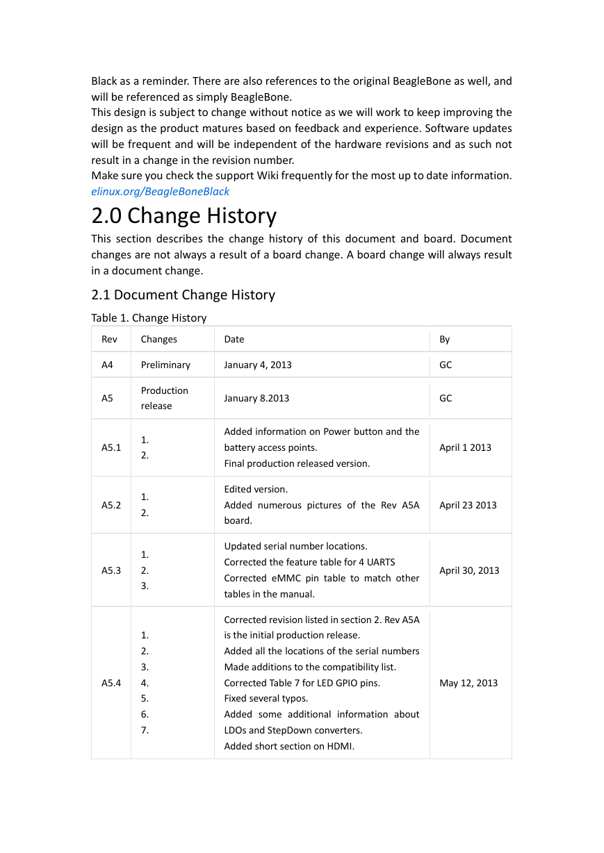
Table 1. Change History
Rev
Changes
Date
A4
Preliminary
January 4, 2013
A5
Production
release
January 8.2013
A5.1
A5.2
A5.3
A5.4
1.
2.
1.
2.
1.
2.
3.
1.
2.
3.
4.
5.
6.
7.
Added information on Power button and the
battery access points.
Final production released version.
Edited version.
Added numerous pictures of the Rev A5A
board.
Updated serial number locations.
Corrected the feature table for 4 UARTS
Corrected eMMC pin table to match other
tables in the manual.
Corrected revision listed in section 2. Rev A5A
is the initial production release.
Added all the locations of the serial numbers
Made additions to the compatibility list.
Corrected Table 7 for LED GPIO pins.
Fixed several typos.
Added some additional information about
LDOs and StepDown converters.
Added short section on HDMI.
By
GC
GC
April 1 2013
April 23 2013
April 30, 2013
May 12, 2013
�






 2023年江西萍乡中考道德与法治真题及答案.doc
 2012年重庆南川中考生物真题及答案.doc
 2013年江西师范大学地理学综合及文艺理论基础考研真题.doc
 2020年四川甘孜小升初语文真题及答案I卷.doc
 2020年注册岩土工程师专业基础考试真题及答案.doc
 2023-2024学年福建省厦门市九年级上学期数学月考试题及答案.doc
 2021-2022学年辽宁省沈阳市大东区九年级上学期语文期末试题及答案.doc
 2022-2023学年北京东城区初三第一学期物理期末试卷及答案.doc
 2018上半年江西教师资格初中地理学科知识与教学能力真题及答案.doc
 2012年河北国家公务员申论考试真题及答案-省级.doc
 2020-2021学年江苏省扬州市江都区邵樊片九年级上学期数学第一次质量检测试题及答案.doc
 2022下半年黑龙江教师资格证中学综合素质真题及答案.doc