Solutions Manual to Accompany
SEMICONDUCTOR DEVICES
Physics and Technology
2nd Edition
S. M. SZE
UMC Chair Professor
National Chiao Tung University
National Nano Device Laboratories
Hsinchu, Taiwan
New York. Chicester / Weinheim / Brisband / Singapore / Toronto
John Wiley and Sons, Inc
1
�
Contents
Ch.1 Introduction--------------------------------------------------------------------- 0
Ch.2 Energy Bands and Carrier Concentration -------------------------------------- 1
Ch.3 Carrier Transport Phenomena -------------------------------------------------- 7
Ch.4 p-n Junction -------------------------------------------------------------------- 16
Ch.5 Bipolar Transistor and Related Devices---------------------------------------- 32
Ch.6 MOSFET and Related Devices------------------------------------------------- 48
Ch.7 MESFET and Related Devices ------------------------------------------------- 60
Ch.8 Microwave Diode, Quantum-Effect and Hot-Electron Devices --------------- 68
Ch.9 Photonic Devices ------------------------------------------------------------- 73
Ch.10 Crystal Growth and Epitaxy--------------------------------------------------- 83
Ch.11 Film Formation---------------------------------------------------------------- 92
Ch.12 Lithography and Etching ------------------------------------------------------ 99
Ch.13 Impurity Doping--------------------------------------------------------------- 105
Ch.14 Integrated Devices------------------------------------------------------------- 113
0
�
CHAPTER 2
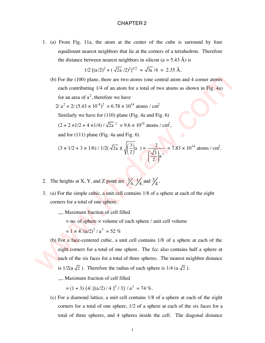
1. (a) From Fig. 11a, the atom at the center of the cube is surround by four
equidistant nearest neighbors that lie at the corners of a tetrahedron. Therefore
the distance between nearest neighbors in silicon (a = 5.43 Å) is
1/2 [(a/2)2 + (
a2 /2)2]1/2 =
a3 /4 = 2.35 Å.
(b) For the (100) plane, there are two atoms (one central atom and 4 corner atoms
each contributing 1/4 of an atom for a total of two atoms as shown in Fig. 4a)
for an area of a2, therefore we have
2/ a2 = 2/ (5.43 × 10⁻⁸)2 = 6.78 × 10¹⁴ atoms / cm2
Similarly we have for (110) plane (Fig. 4a and Fig. 6)
a2 2 = 9.6 × 10¹⁵ atoms / cm2,
(2 + 2 ×1/2 + 4 ×1/4) /
and for (111) plane (Fig. 4a and Fig. 6)
(3 × 1/2 + 3 × 1/6) / 1/2(
a2 )(
a
) =
3
2
2
3
2
a
2
= 7.83 × 10¹⁴ atoms / cm2.
2. The heights at X, Y, and Z point are
3
,4
3 .
1 and 4
,4
3. (a) For the simple cubic, a unit cell contains 1/8 of a sphere at each of the eight
corners for a total of one sphere.
4 Maximum fraction of cell filled
= no. of sphere × volume of each sphere / unit cell volume
= 1 × 4(a/2)3 / a3 = 52 %
(b) For a face-centered cubic, a unit cell contains 1/8 of a sphere at each of the
eight corners for a total of one sphere. The fcc also contains half a sphere at
each of the six faces for a total of three spheres. The nearest neighbor distance
is 1/2(a 2 ). Therefore the radius of each sphere is 1/4 (a 2 ).
4 Maximum fraction of cell filled
= (1 + 3) {4[(a/2) / 4 ]3 / 3} / a3 = 74 %.
(c) For a diamond lattice, a unit cell contains 1/8 of a sphere at each of the eight
corners for a total of one sphere, 1/2 of a sphere at each of the six faces for a
total of three spheres, and 4 spheres inside the cell. The diagonal distance
1
ł
Ł
ł
Ł
�
4 cosŁ =
Ł= cos-1 (
1-
3
1-
3
) = 109.470 .
between (1/2, 0, 0) and (1/4, 1/4, 1/4) shown in Fig. 9a is
D =
1
2
a
2
2
+
a
2
2
+
a
2
2
=
a
4
3
The radius of the sphere is D/2 =
a
8
4 Maximum fraction of cell filled
3
= (1 + 3 + 4)
ap
4
8
3
3
3
/ a3 = 3 / 16 = 34 %.
This is a relatively low percentage compared to other lattice structures.
1d =
2d =
4.
3d =
1d + 2d + 3d + 4d = 0
1d • ( 1d + 2d + 3d + 4d ) =
1d + 1d •
2d + 1d • 3d +
2
4d = d
1d • 0 = 0
4d = 0
1d •
4d2+ d2 cosŁ12 + d2cosŁ13 + d2cosŁ14 = d2 +3 d2 cosŁ= 0
5. Taking the reciprocals of these intercepts we get 1/2, 1/3 and 1/4. The smallest
three integers having the same ratio are 6, 4, and 3. The plane is referred to as
(643) plane.
6. (a) The lattice constant for GaAs is 5.65 Å, and the atomic weights of Ga and As
are 69.72 and 74.92 g/mole, respectively. There are four gallium atoms and
four arsenic atoms per unit cell, therefore
4/a3 = 4/ (5.65 × 10⁻⁸)3 = 2.22 × 10²² Ga or As atoms/cm2,
Density = (no. of atoms/cm3 × atomic weight) / Avogadro constant
= 2.22 × 10²²(69.72 + 74.92) / 6.02 × 1023 = 5.33 g / cm3.
(b) If GaAs is doped with Sn and Sn atoms displace Ga atoms, donors are
formed, because Sn has four valence electrons while Ga has only three. The
resulting semiconductor is n-type.
7. (a) The melting temperature for Si is 1412 ºC, and for SiO 2 is 1600 ºC. Therefore,
SiO2 has higher melting temperature. It is more difficult to break the Si-O
bond than the Si-Si bond.
(b) The seed crystal is used to initiated the growth of the ingot with the correct
crystal orientation.
(c) The crystal orientation determines the semiconductor’s chemical and electrical
2
ł
Ł
ł
Ł
ł
Ł
œ
ß
ø
Œ
º
Ø
ł
Ł
�
properties, such as the etch rate, trap density, breakage plane etc.
(d) The temperating of the crusible and the pull rate.
8. Eg (T) = 1.17 –
\
4.73x10
+
T
(
4
T
636)
2
for Si
Eg ( 100 K) = 1.163 eV , and Eg (600 K) = 1.032 eV
Eg(T) = 1.519 –
\ Eg( 100 K) = 1.501 eV, and Eg (600 K) = 1.277 eV .
for GaAs
T
(
+
5.405x10
2
4
T
204)
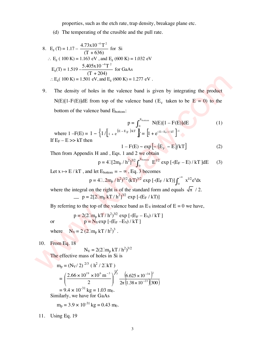
9.
The density of holes in the valence band is given by integrating the product
N(E)[1-F(E)]dE from top of the valence band (
VE taken to be E = 0) to the
bottom of the valence band Ebottom:
bottom
{
/1
where 1 –F(E) =
1
If EF – E >> kT then
N(E)[1 – F(E)]dE (1)
+
(e1
[
(
E F
Then from Appendix H and , Eqs. 1 and 2 we obtain
] 1
]kT
)
(2)
1 – F(E) ~ exp
= [
FEE -
[
EE
E
kT
e
/)
F
(
+
1
E
p =
}/kT
]
)
0
p = 4[2mp / h2]3/2
E
bottom
0
E1/2 exp [-(EF – E) / kT ]dE (3)
Let x a E / kT , and let Ebottom =
, Eq. 3 becomes
x1/2exdx
where the integral on the right is of the standard form and equals p / 2.
p = 4(2mp / h2)3/2 (kT)3/2 exp [-(EF / kT)]
0
-
4 p = 2[2mp kT / h2]3/2 exp [-(EF / kT)]
By referring to the top of the valence band as EV instead of E = 0 we have,
p = 2(2mp kT / h2)3/2 exp [-(EF – EV) / kT ]
or
where NV = 2 (2mp kT / h2)3 .
p = NV exp [-(EF –EV) / kT ]
10. From Eq. 18
NV = 2(2mp kT / h2)3/2
The effective mass of holes in Si is
mp = (NV / 2) 2/3 ( h2 / 2kT )
(
.
625
6
(
p
.
3812
34
2
)
)(
300
)
10
10
23
=
66.2
19
10
6
m10
3
2
3
2
= 9.4 × 10⁻³¹ kg = 1.03 m0.
Similarly, we have for GaAs
mp = 3.9 × 10⁻³¹ kg = 0.43 m0.
11. Using Eq. 19
3
-
-
-
-
-
-
-
¥
-
¥
ł
Ł
·
·
-
-
-
·
·
�
=
(
E
C
+
Ei
E
V
2)
(
kT
+
)
ln2
(
NN
V
C
)
= (EC+ EV)/ 2 + (3kT / 4) ln
(
p mm
n
)6)(
2
3
(1)
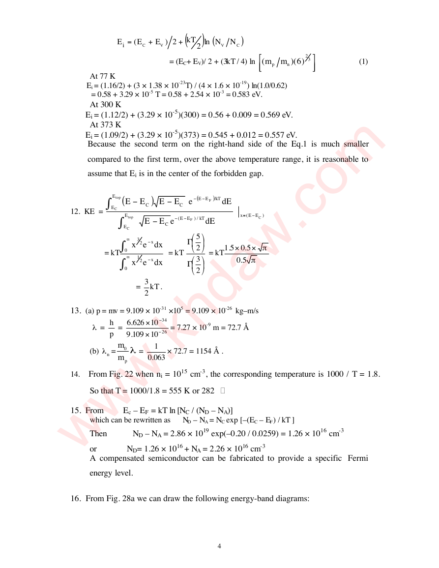
At 77 K
Ei = (1.16/2) + (3 × 1.38 × 10-23T) / (4 × 1.6 × 10-19) ln(1.0/0.62)
= 0.58 + 3.29 × 10⁻⁵ T = 0.58 + 2.54 × 10-3 = 0.583 eV.
Ei = (1.12/2) + (3.29 × 10⁻⁵)(300) = 0.56 + 0.009 = 0.569 eV.
At 300 K
At 373 K
Ei = (1.09/2) + (3.29 × 10⁻⁵)(373) = 0.545 + 0.012 = 0.557 eV.
Because the second term on the right-hand side of the Eq.1 is much smaller
compared to the first term, over the above temperature range, it is reasonable to
assume that Ei is in the center of the forbidden gap.
12. KE =
(
E
top
E
C
)
EE
C
EE
C
e
(
EE
F
)
kT
/
d
E
E
top
E
C
eEE
C
(
EE
F
/)
kT
d
E
x
(
EE
)
C
= kT
5
2
3
2
= kT
3
1
x
x
2
x
de
x
2
x
de
x
0
0
=
3
2
kT
.
= kT
.
.
5051
.
50
p
p
13. (a) p = mv = 9.109 × 10-31 ×105 = 9.109 × 10⁻²⁶ kg–m/s
l =
h
p
(b)
nl =
=
.
6
626
.
109
9
m0
pm
l
=
34
26
10
10
1
063
.
0
= 7.27 × 10⁻⁹ m = 72.7 Å
× 72.7 = 1154 Å .
14. From Fig. 22 when ni = 1015 cm-3, the corresponding temperature is 1000 / T = 1.8.
So that T = 1000/1.8 = 555 K or 282 .
15. From Ec – EF = kT ln [NC / (ND – NA)]
which can be rewritten as ND – NA = NC exp [–(EC – EF) / kT ]
Then ND – NA = 2.86 × 10¹⁹ exp(–0.20 / 0.0259) = 1.26 × 1016 cm-3
or ND= 1.26 × 10¹⁶ + NA = 2.26 × 1016 cm-3
A compensated semiconductor can be fabricated to provide a specific Fermi
energy level.
16. From Fig. 28a we can draw the following energy-band diagrams:
4
œ
ß
ø
Œ
º
Ø
-
”
-
-
-
-
-
-
-
¥
-
¥
-
ł
Ł
G
ł
Ł
G
·
·
-
-
·
·
�
17.
(a) The ionization energy for boron in Si is 0.045 eV. At 300 K, all boron
impurities are ionized. Thus pp = NA = 1015 cm-3
np = ni
2 / nA = (9.65 × 10⁹)2 / 1015 = 9.3 × 104 cm-3.
The Fermi level measured from the top of the valence band is given by:
EF – EV = kT ln(N V/ND) = 0.0259 ln (2.66 × 10¹⁹ / 1015) = 0.26 eV
(b) The boron atoms compensate the arsenic atoms; we have
pp = NA – ND = 3 × 10¹⁶ – 2.9 × 1016 = 1015 cm-3
Since pp is the same as given in (a), the values for np and EF are the same as
in (a). However, the mobilities and resistivities for these two samples are
different.
18. Since ND >> ni, we can approximate n0 = ND and
p0 = ni
2 / n0 = 9.3 ×10¹⁹ / 1017 = 9.3 × 102 cm-3
From n0 = ni exp
E
F
E
i
kT
,
we have
EF – Ei = kT ln (n0 / ni) = 0.0259 ln (1017 / 9.65 × 10⁹) = 0.42 eV
The resulting flat band diagram is :
5
ł
Ł
-
�
19. Assuming complete ionization, the Fermi level measured from the intrinsic
Fermi level is 0.35 eV for 1015 cm-3, 0.45 eV for 1017 cm-3, and 0.54 eV for 1019
cm-3.
The number of electrons that are ionized is given by
]
ND[1 – F(ED)] = ND / [1 + e
n @
Tk
E
E
(
)
D
/
F
Using the Fermi levels given above, we obtain the number of ionized donors as
n = 1015 cm-3 for ND = 1015 cm-3
n = 0.93 × 1017 cm-3 for ND = 1017 cm-3
n = 0.27 × 1019 cm-3 for ND = 1019 cm-3
Therefore, the assumption of complete ionization is valid only for the case of
1015 cm-3.
16
16
E
10
E
(
=
10
-+
-+
e
e1
= 5.33 × 1015 cm-3
kT
/)
D
F
0
.
135
20. ND
=
1
+ =
1
1016
1
+
145
.
1
The neutral donor = 1016 – 5.33 ×1015 cm-3 = 4.67 × 1015 cm-3
4 The ratio of
N O
D
+
N
D
=
.
764
.
335
= 0.876 .
6
-
-
-
�



 2023年江西萍乡中考道德与法治真题及答案.doc
 2012年重庆南川中考生物真题及答案.doc
 2013年江西师范大学地理学综合及文艺理论基础考研真题.doc
 2020年四川甘孜小升初语文真题及答案I卷.doc
 2020年注册岩土工程师专业基础考试真题及答案.doc
 2023-2024学年福建省厦门市九年级上学期数学月考试题及答案.doc
 2021-2022学年辽宁省沈阳市大东区九年级上学期语文期末试题及答案.doc
 2022-2023学年北京东城区初三第一学期物理期末试卷及答案.doc
 2018上半年江西教师资格初中地理学科知识与教学能力真题及答案.doc
 2012年河北国家公务员申论考试真题及答案-省级.doc
 2020-2021学年江苏省扬州市江都区邵樊片九年级上学期数学第一次质量检测试题及答案.doc
 2022下半年黑龙江教师资格证中学综合素质真题及答案.doc