High Speed, Half-Duplex iCoupler®
Isolated RS-485 Transceiver
ADM2486
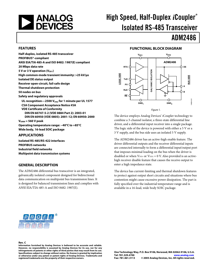
FUNCTIONAL BLOCK DIAGRAM
VDD1
VDD2
ADM2486
RTS
TxD
PV
RxD
RE
I
N
O
T
A
L
O
S
I
I
C
N
A
V
L
A
G
DE
A
B
I
E
D
S
S
U
B
I
E
D
S
C
G
O
L
I
GND1
GND2
Figure 1.
1
0
0
-
4
0
6
4
0
The device employs Analog Devices’ iCoupler technology to
combine a 3-channel isolator, a three-state differential line
driver, and a differential input receiver into a single package.
The logic side of the device is powered with either a 5 V or a
3 V supply, and the bus side uses an isolated 5 V supply.
The ADM2486 driver has an active-high enable feature. The
driver differential outputs and the receiver differential inputs
are connected internally to form a differential input/output port
that imposes minimal loading on the bus when the driver is
disabled or when VDD1 or VDD2 = 0 V. Also provided is an active-
high receiver disable feature that causes the receive output to
enter a high impedance state.
The device has current-limiting and thermal shutdown features
to protect against output short circuits and situations where bus
contention might cause excessive power dissipation. The part is
fully specified over the industrial temperature range and is
available in a 16-lead, wide body SOIC package.
FEATURES
Half-duplex, isolated RS-485 transceiver
PROFIBUS®-compliant
ANSI EIA/TIA 485-A and ISO 8482: 1987(E) compliant
20 Mbps data rate
5 V or 3 V operation (VDD1)
High common-mode transient immunity: >25 kV/μs
Isolated DE status output
Receiver open-circuit, fail-safe design
Thermal shutdown protection
50 nodes on bus
Safety and regulatory approvals
UL recognition—2500 Vrms for 1 minute per UL 1577
CSA Component Acceptance Notice #5A
VDE Certificate of Conformity
DIN EN 60747-5-2 (VDE 0884 Part 2): 2003-01
DIN EN 60950 (VDE 0805): 2001-12; EN 60950: 2000
VIORM = 560 V peak
Operating temperature range: −40°C to +85°C
Wide body, 16-lead SOIC package
APPLICATIONS
Isolated RS-485/RS-422 interfaces
PROFIBUS networks
Industrial field networks
Multipoint data transmission systems
GENERAL DESCRIPTION
The ADM2486 differential bus transceiver is an integrated,
galvanically isolated component designed for bidirectional
data communication on multipoint bus transmission lines. It
is designed for balanced transmission lines and complies with
ANSI EIA/TIA-485-A and ISO 8482: 1987(E).
Rev. C
Information furnished by Analog Devices is believed to be accurate and reliable.
However, no responsibility is assumed by Analog Devices for its use, nor for any
infringements of patents or other rights of third parties that may result from its use.
Specifications subject to change without notice. No license is granted by implication
or otherwise under any patent or patent rights of Analog Devices. Trademarks and
registered trademarks are the property of their respective owners.
One Technology Way, P.O. Box 9106, Norwood, MA 02062-9106, U.S.A.
Tel: 781.329.4700
www.analog.com
© 2005 Analog Devices, Inc. All rights reserved.
Fax: 781.461.3113
�
Circuit Description......................................................................... 14
Electrical Isolation...................................................................... 14
Truth Tables................................................................................. 14
Power-Up/Power-Down Thresholds ....................................... 14
Thermal Shutdown .................................................................... 15
Receiver Fail-Safe Inputs ........................................................... 15
Magnetic Field Immunity.......................................................... 15
Applications Information .............................................................. 16
Power_Valid Input ..................................................................... 16
Isolated Power Supply Circuit .................................................. 17
Outline Dimensions....................................................................... 18
Ordering Guide .......................................................................... 18
ADM2486
TABLE OF CONTENTS
Specifications..................................................................................... 3
Timing Specifications....................................................................... 5
Absolute Maximum Ratings............................................................ 6
ESD Caution.................................................................................. 6
ADM2486 Characteristics ............................................................... 7
Package Characteristics ............................................................... 7
Regulatory Information............................................................... 7
Insulation and Safety-Related Specifications............................ 7
VDE 0884 Insulation Characteristics ........................................ 8
Pin Configuration and Function Descriptions............................. 9
Test Circuits..................................................................................... 10
Switching Characteristics .............................................................. 11
Typical Performance Characteristics ........................................... 12
REVISION HISTORY
3/05—Rev. B to Rev. C
Change to Package Characteristics................................................. 7
Changes to Figure 12, Figure 14, and Figure 15 ......................... 11
Change to Power_Valid Input Section......................................... 16
1/05—Rev. A to Rev. B
Added PROFIBUS logo ................................................................... 1
11/04—Rev. 0 to Rev. A
Changes to Figure 1.......................................................................... 1
Changes to Figure 6........................................................................ 10
Added Figure 22 through Figure 25............................................. 13
Updated Outline Dimensions....................................................... 18
Changes to Ordering Guide .......................................................... 18
Rev. C | Page 2 of 20
�
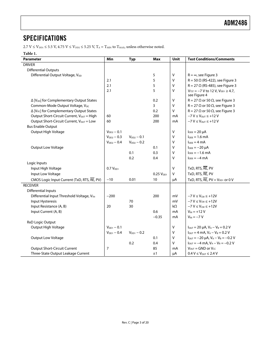
ADM2486
SPECIFICATIONS
2.7 V ≤ VDD1 ≤ 5.5 V, 4.75 V ≤ VDD2 ≤ 5.25 V, TA = TMIN to TMAX, unless otherwise noted.
Table 1.
Parameter
DRIVER
Min
2.1
2.1
2.1
Typ
Differential Outputs
Differential Output Voltage, VOD
∆ |VOD| for Complementary Output States
Common-Mode Output Voltage, VOC
∆ |VOC| for Complementary Output States
Output Short-Circuit Current, VOUT = High
Output Short-Circuit Current, VOUT = Low
Bus Enable Output
Output High Voltage
Output Low Voltage
Logic Inputs
Input High Voltage
Input Low Voltage
CMOS Logic Input Current (TxD, RTS, RE, PV)
RECEIVER
Differential Inputs
Differential Input Threshold Voltage, VTH
Input Hysteresis
Input Resistance (A, B)
Input Current (A, B)
RxD Logic Output
Output High Voltage
Output Low Voltage
Output Short-Circuit Current
Three-State Output Leakage Current
Unit
V
V
V
V
V
V
V
mA
mA
V
V
V
V
V
V
V
V
µA
mV
mV
kΩ
mA
mA
V
V
V
V
mA
µA
Test Conditions/Comments
R = ∞, see Figure 3
R = 50 Ω (RS-422), see Figure 3
R = 27 Ω (RS-485), see Figure 3
VTST = −7 V to 12 V, VDD1 ≥ 4.7,
see Figure 4
R = 27 Ω or 50 Ω, see Figure 3
R = 27 Ω or 50 Ω, see Figure 3
R = 27 Ω or 50 Ω, see Figure 3
−7 V ≤ VOUT ≤ +12 V
−7 V ≤ VOUT ≤ +12 V
IODE = 20 µA
IODE = 1.6 mA
IODE = 4 mA
IODE = −20 µA
IODE = −1.6 mA
IODE = −4 mA
TxD, RTS, RE, PV
TxD, RTS, RE, PV
TxD, RTS, RE, PV = VDD1 or 0 V
−7 V ≤ VCM ≤ +12V
−7 V ≤ VCM ≤ +12V
−7 V ≤ VCM ≤ +12V
VIN = +12 V
VIN = −7 V
IOUT = 20 µA, VA − VB = 0.2 V
IOUT = 4 mA, VA − VB = 0.2 V
IOUT = −20 µA, VA − VB = −0.2 V
IOUT = −4 mA, VA − VB = −0.2 V
VOUT = GND or VCC
0.4 V ≤ VOUT ≤ 2.4 V
Max
5
5
5
5
60
60
VDD2 − 0.1
VDD2 − 0.3
VDD2 − 0.4
0.7 VDD1
−10
−200
20
VDD1 − 0.1
VDD1 − 0.4
7
VDD2 − 0.1
VDD2 − 0.2
0.1
0.2
0.01
70
30
VDD1 − 0.2
0.2
0.2
3
0.2
200
200
0.1
0.3
0.4
0.25 VDD1
10
200
0.6
−0.35
0.1
0.4
85
±1
Rev. C | Page 3 of 20
�
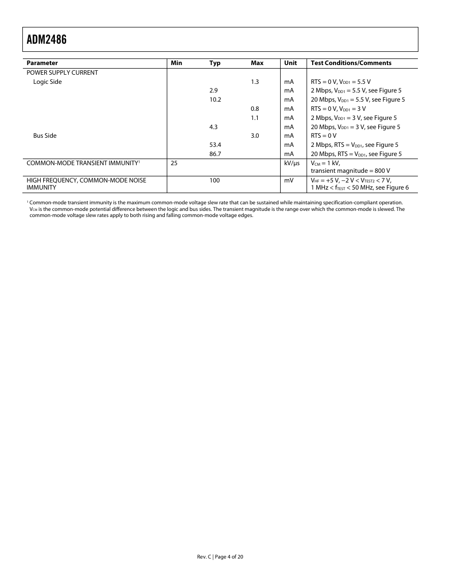
ADM2486
Parameter
POWER SUPPLY CURRENT
Logic Side
Bus Side
COMMON-MODE TRANSIENT IMMUNITY1
HIGH FREQUENCY, COMMON-MODE NOISE
IMMUNITY
Min
25
Typ
2.9
10.2
4.3
53.4
86.7
100
Max
1.3
0.8
1.1
3.0
Unit
mA
mA
mA
mA
mA
mA
mA
mA
mA
kV/µs
mV
Test Conditions/Comments
RTS = 0 V, VDD1 = 5.5 V
2 Mbps, VDD1 = 5.5 V, see Figure 5
20 Mbps, VDD1 = 5.5 V, see Figure 5
RTS = 0 V, VDD1 = 3 V
2 Mbps, VDD1 = 3 V, see Figure 5
20 Mbps, VDD1 = 3 V, see Figure 5
RTS = 0 V
2 Mbps, RTS = VDD1, see Figure 5
20 Mbps, RTS = VDD1, see Figure 5
VCM = 1 kV,
transient magnitude = 800 V
VHF = +5 V, −2 V < VTEST2 < 7 V,
1 MHz < fTEST < 50 MHz, see Figure 6
1 Common-mode transient immunity is the maximum common-mode voltage slew rate that can be sustained while maintaining specification-compliant operation.
VCM is the common-mode potential difference between the logic and bus sides. The transient magnitude is the range over which the common-mode is slewed. The
common-mode voltage slew rates apply to both rising and falling common-mode voltage edges.
Rev. C | Page 4 of 20
�
Maximum Data Rate
Propagation Delay, tPLH, tPHL
RTS-to-DE Propagation Delay
Pulse Width Distortion, tPWD
Switching Skew, tSKEW
Rise/Fall Time, tR, tF
Enable Time
Disable Time
Enable Skew, |tAZH − tBZL|, |tAZL − tBZH|
Disable Skew, |tAHZ − tBLZ|, |tALZ − tBHZ|
RECEIVER
Propagation Delay, tPLH, tPHL
Differential Skew, tSKEW
Enable Time
Disable Time
POWER_VALID INPUT
Enable Time
Disable Time
Test Conditions/Comments
RLDIFF = 54 Ω, CL1 = CL2 = 100 pF, see Figure 7
See Figure 8
RLDIFF = 54 Ω, CL1 = CL2 = 100 pF, see Figure 7 and
Figure 12
RLDIFF = 54 Ω, CL1 = CL2 = 100 pF, see Figure 7 and
Figure 12
RLDIFF = 54 Ω, CL1 = CL2 = 100 pF, see Figure 7 and
Figure 12
See Figure 9 and Figure 14
See Figure 9 and Figure 14
See Figure 9 and Figure 14
See Figure 9 and Figure 14
CL = 15 pF, see Figure 10 and Figure 13
CL = 15 pF, see Figure 10 and Figure 13
RL = 1 kΩ, CL = 15 pF, see Figure 11 and Figure 15
RL = 1 kΩ, CL = 15 pF, see Figure 11 and Figure 15
ADM2486
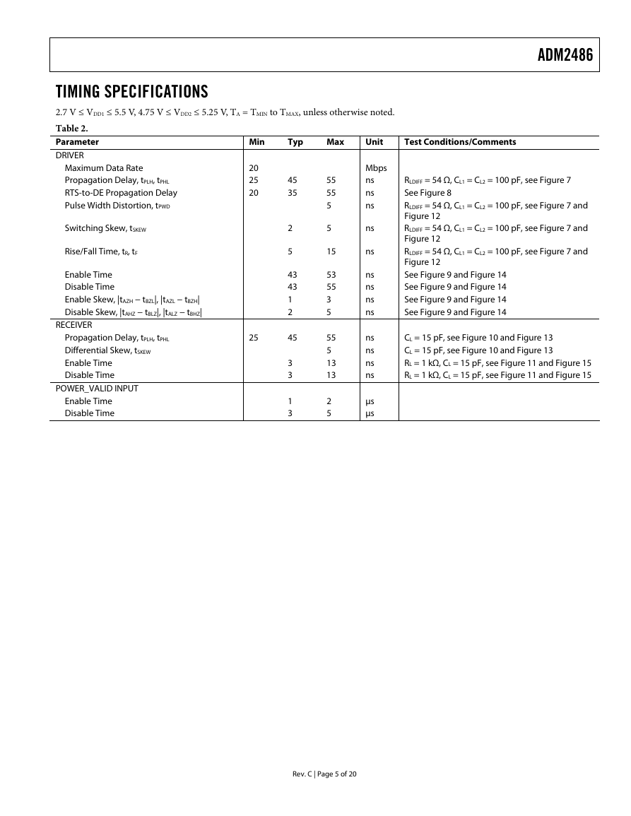
TIMING SPECIFICATIONS
2.7 V ≤ VDD1 ≤ 5.5 V, 4.75 V ≤ VDD2 ≤ 5.25 V, TA = TMIN to TMAX, unless otherwise noted.
Table 2.
Parameter
DRIVER
Min
20
25
20
Typ
45
35
Max
55
55
5
Unit
Mbps
ns
ns
ns
25
2
5
43
43
1
2
45
3
3
1
3
5
15
53
55
3
5
55
5
13
13
2
5
ns
ns
ns
ns
ns
ns
ns
ns
ns
ns
µs
µs
Rev. C | Page 5 of 20
�
ADM2486
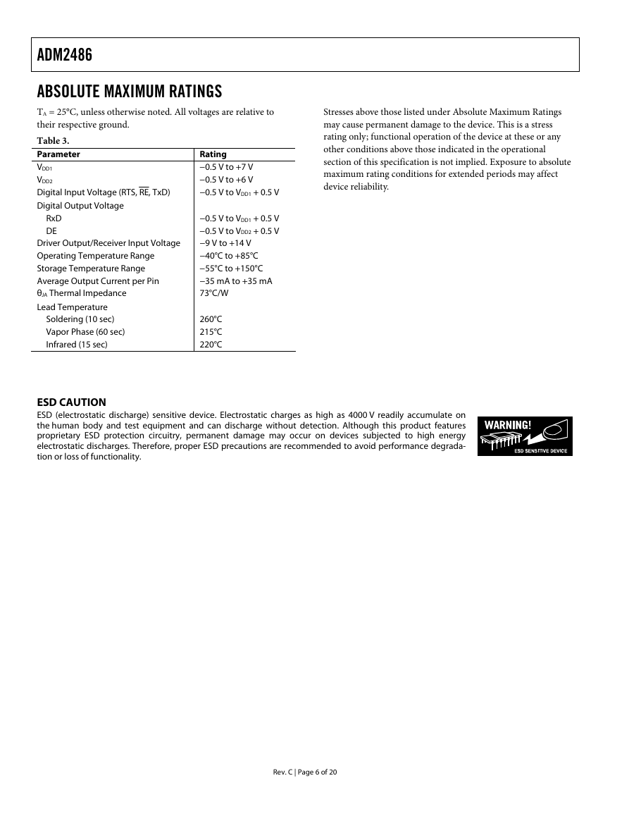
ABSOLUTE MAXIMUM RATINGS
TA = 25°C, unless otherwise noted. All voltages are relative to
their respective ground.
Table 3.
Parameter
VDD1
VDD2
Digital Input Voltage (RTS, RE, TxD)
Digital Output Voltage
Rating
−0.5 V to +7 V
−0.5 V to +6 V
−0.5 V to VDD1 + 0.5 V
−0.5 V to VDD1 + 0.5 V
−0.5 V to VDD2 + 0.5 V
−9 V to +14 V
−40°C to +85°C
−55°C to +150°C
−35 mA to +35 mA
73°C/W
260°C
215°C
220°C
RxD
DE
Driver Output/Receiver Input Voltage
Operating Temperature Range
Storage Temperature Range
Average Output Current per Pin
θJA Thermal Impedance
Lead Temperature
Soldering (10 sec)
Vapor Phase (60 sec)
Infrared (15 sec)
Stresses above those listed under Absolute Maximum Ratings
may cause permanent damage to the device. This is a stress
rating only; functional operation of the device at these or any
other conditions above those indicated in the operational
section of this specification is not implied. Exposure to absolute
maximum rating conditions for extended periods may affect
device reliability.
ESD CAUTION
ESD (electrostatic discharge) sensitive device. Electrostatic charges as high as 4000 V readily accumulate on
the human body and test equipment and can discharge without detection. Although this product features
proprietary ESD protection circuitry, permanent damage may occur on devices subjected to high energy
electrostatic discharges. Therefore, proper ESD precautions are recommended to avoid performance degrada-
tion or loss of functionality.
Rev. C | Page 6 of 20
�
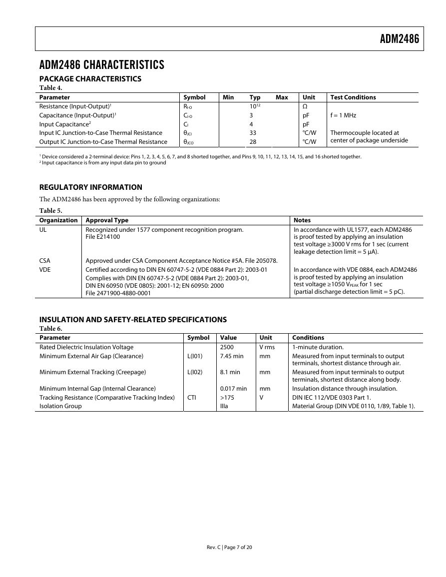
ADM2486 CHARACTERISTICS
PACKAGE CHARACTERISTICS
Table 4.
Parameter
Resistance (Input-Output)1
Capacitance (Input-Output)1
Input Capacitance2
Input IC Junction-to-Case Thermal Resistance
Output IC Junction-to-Case Thermal Resistance
ADM2486
Symbol
RI-O
CI-O
CI
θJCI
θJCO
Min
Typ
1012
3
4
33
28
Max
Unit
Ω
pF
pF
°C/W
°C/W
Test Conditions
f = 1 MHz
Thermocouple located at
center of package underside
1 Device considered a 2-terminal device: Pins 1, 2, 3, 4, 5, 6, 7, and 8 shorted together, and Pins 9, 10, 11, 12, 13, 14, 15, and 16 shorted together.
2 Input capacitance is from any input data pin to ground
REGULATORY INFORMATION
The ADM2486 has been approved by the following organizations:
Table 5.
Organization Approval Type
UL
Recognized under 1577 component recognition program.
File E214100
CSA
VDE
Approved under CSA Component Acceptance Notice #5A. File 205078.
Certified according to DIN EN 60747-5-2 (VDE 0884 Part 2): 2003-01
Complies with DIN EN 60747-5-2 (VDE 0884 Part 2): 2003-01,
DIN EN 60950 (VDE 0805): 2001-12; EN 60950: 2000
File 2471900-4880-0001
Notes
In accordance with UL1577, each ADM2486
is proof tested by applying an insulation
test voltage ≥3000 V rms for 1 sec (current
leakage detection limit = 5 µA).
In accordance with VDE 0884, each ADM2486
is proof tested by applying an insulation
test voltage ≥1050 VPEAK for 1 sec
(partial discharge detection limit = 5 pC).
Unit
V rms
mm
mm
mm
V
Conditions
1-minute duration.
Measured from input terminals to output
terminals, shortest distance through air.
Measured from input terminals to output
terminals, shortest distance along body.
Insulation distance through insulation.
DIN IEC 112/VDE 0303 Part 1.
Material Group (DIN VDE 0110, 1/89, Table 1).
INSULATION AND SAFETY-RELATED SPECIFICATIONS
Table 6.
Parameter
Rated Dielectric Insulation Voltage
Minimum External Air Gap (Clearance)
Symbol
L(I01)
Value
2500
7.45 min
Minimum External Tracking (Creepage)
L(I02)
8.1 min
Minimum Internal Gap (Internal Clearance)
Tracking Resistance (Comparative Tracking Index)
Isolation Group
CTI
0.017 min
>175
IIIa
Rev. C | Page 7 of 20
�
ADM2486
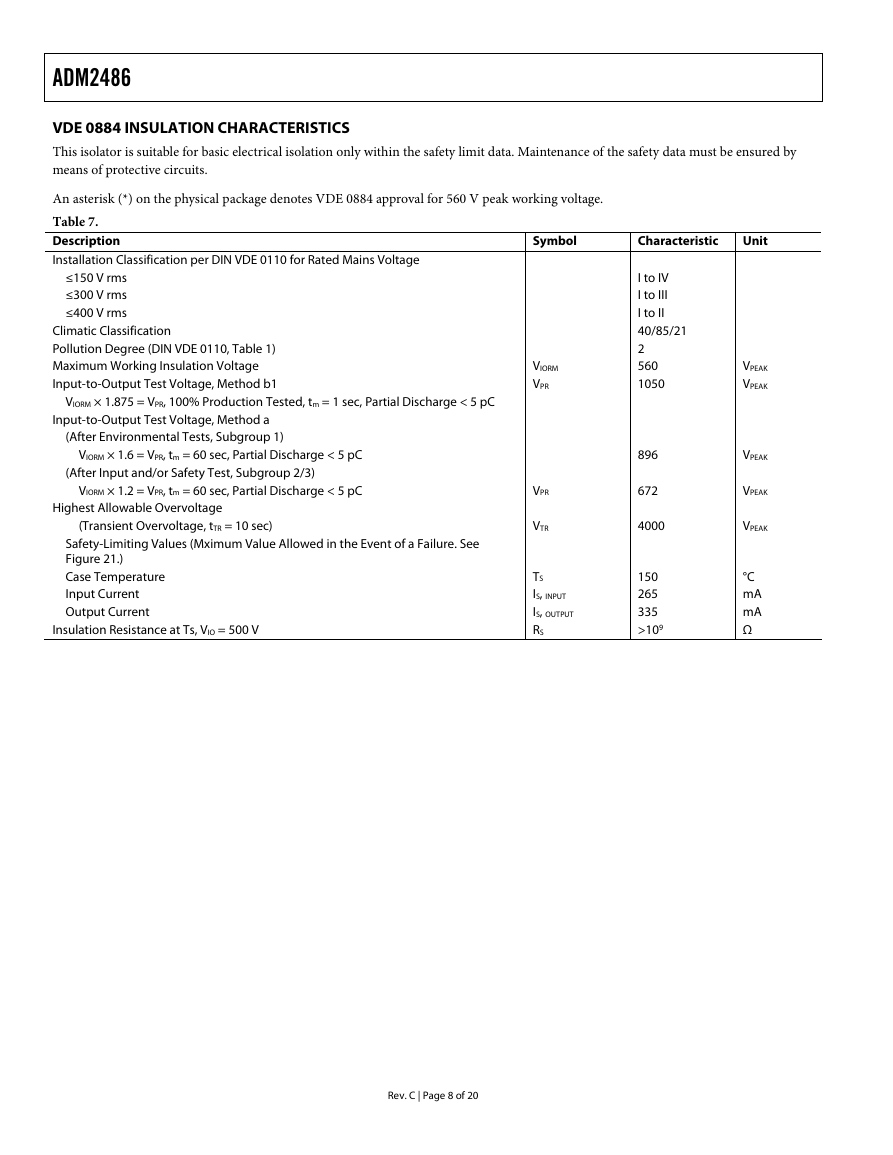
VDE 0884 INSULATION CHARACTERISTICS
This isolator is suitable for basic electrical isolation only within the safety limit data. Maintenance of the safety data must be ensured by
means of protective circuits.
An asterisk (*) on the physical package denotes VDE 0884 approval for 560 V peak working voltage.
Table 7.
Description
Installation Classification per DIN VDE 0110 for Rated Mains Voltage
Symbol
VIORM
VPR
VPR
VTR
Characteristic
I to IV
I to III
I to II
40/85/21
2
560
1050
896
672
4000
Unit
VPEAK
VPEAK
VPEAK
VPEAK
VPEAK
°C
mA
mA
Ω
TS
IS, INPUT
IS, OUTPUT
RS
150
265
335
>109
≤150 V rms
≤300 V rms
≤400 V rms
Climatic Classification
Pollution Degree (DIN VDE 0110, Table 1)
Maximum Working Insulation Voltage
Input-to-Output Test Voltage, Method b1
VIORM × 1.875 = VPR, 100% Production Tested, tm = 1 sec, Partial Discharge < 5 pC
Input-to-Output Test Voltage, Method a
(After Environmental Tests, Subgroup 1)
VIORM × 1.6 = VPR, tm = 60 sec, Partial Discharge < 5 pC
(After Input and/or Safety Test, Subgroup 2/3)
VIORM × 1.2 = VPR, tm = 60 sec, Partial Discharge < 5 pC
Highest Allowable Overvoltage
(Transient Overvoltage, tTR = 10 sec)
Safety-Limiting Values (Mximum Value Allowed in the Event of a Failure. See
Figure 21.)
Case Temperature
Input Current
Output Current
Insulation Resistance at Ts, VIO = 500 V
Rev. C | Page 8 of 20
�


 2023年江西萍乡中考道德与法治真题及答案.doc
 2012年重庆南川中考生物真题及答案.doc
 2013年江西师范大学地理学综合及文艺理论基础考研真题.doc
 2020年四川甘孜小升初语文真题及答案I卷.doc
 2020年注册岩土工程师专业基础考试真题及答案.doc
 2023-2024学年福建省厦门市九年级上学期数学月考试题及答案.doc
 2021-2022学年辽宁省沈阳市大东区九年级上学期语文期末试题及答案.doc
 2022-2023学年北京东城区初三第一学期物理期末试卷及答案.doc
 2018上半年江西教师资格初中地理学科知识与教学能力真题及答案.doc
 2012年河北国家公务员申论考试真题及答案-省级.doc
 2020-2021学年江苏省扬州市江都区邵樊片九年级上学期数学第一次质量检测试题及答案.doc
 2022下半年黑龙江教师资格证中学综合素质真题及答案.doc