ispLEVER Tutorials
Using the ispXPGA
Floorplanner
Table of Contents
USING THE ISPXPGA FLOORPLANNER ..................................................................3
Task 1: Open the Design ......................................................................................4
Task 2: Open a Floorplanner Design File .............................................................5
Task 3: Tour the Graphical User Interface - The Design Browser ........................6
Task 4: Tour the Graphical User Interface - The Package View ...........................7
Task 5: Tour the Graphical User Interface - The Floorplan View ..........................8
Task 6: Customizing the Floorplanner Display....................................................10
Task 7: Locate an Element with the Design Browser..........................................13
Task 8: Change Pin Assignments.......................................................................17
Task 9: Reassign PFU Block Locations ..............................................................21
Task 10: Set a Placement Region.......................................................................23
Task 11: Use the Query Widget to Find Instances and Nets ..............................26
Task 12: Locate Timing Delay Paths with the Timing Widget .............................29
Task 13: Group Instances with the Design Browser ...........................................31
Task 14: Locate a Group with the Group Widget ................................................34
Congratulations...................................................................................................36
© 2004 Lattice Semiconductor
Tutor7
�
ispLEVER Tutorials
Using the ispXPGA Floorplanner
2
© 2004 Lattice Semiconductor
�
ispLEVER Tutorials
Using the ispXPGA Floorplanner
Using the ispXPGA Floorplanner
This tutorial shows you how to use the Floorplanner to make adjustments to your
ispXPGA design.
Learning Objectives
When you have completed this tutorial, you should be able to:
• Open a Floorplanner design file
• Tour the graphical user interface
• Customize the Floorplanner display
• Locate an element using the Design Browser
• Change pin assignments
• Reassign PFU block locations
• Set a placement region
• Use the Query Widget to find instances and nets
• Locate timing delay paths with the Timing Widget
• Group instances with the Design Browser
• Locate a group with the Group Widget
Time to Complete This Tutorial
The time to complete this tutorial is about 40 minutes.
© 2004 Lattice Semiconductor
3
�
ispLEVER Tutorials
Using the ispXPGA Floorplanner
Task 1: Open the Design
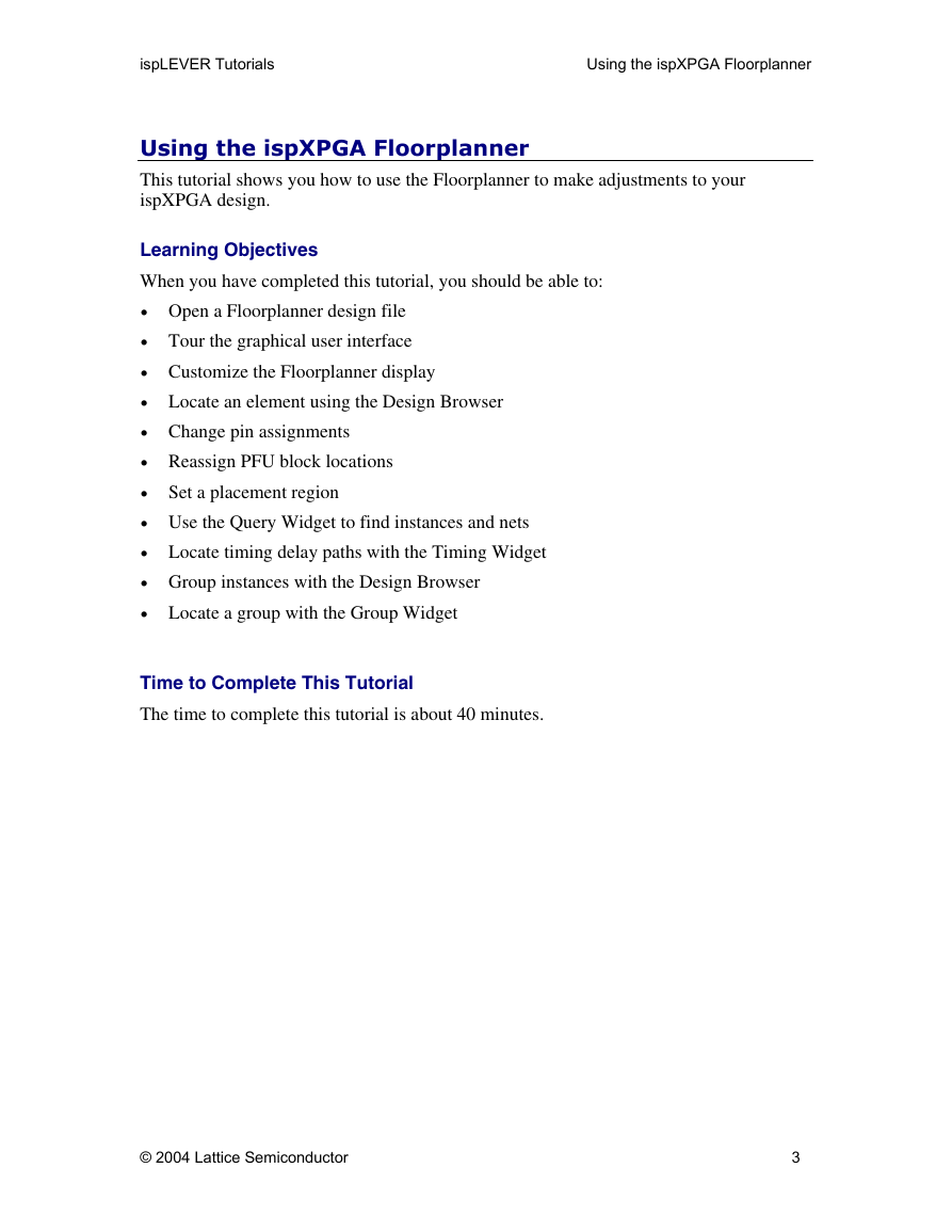
After starting the Project Navigator you can open the tutorial design file.
1. Choose File > Open Example to open the dialog box.
2. Navigate to the tutorial\tutor7 directory.
Note: If you want to preserve the original tutorial design files, save the tutor7 directory to
another location on your computer before proceeding.
3. Select traffic.syn.
4. Click Open.
Note: You can toggle Revision Control on/off by right clicking in the Revision Control window and
selecting either Turn On or Turn Off from the popup menu. For this tutorial, it doesn’t matter.
4
© 2004 Lattice Semiconductor
�
ispLEVER Tutorials
Using the ispXPGA Floorplanner
Task 2: Open a Floorplanner Design File
After an initial Lattice internal database is generated, the Pack & Place Design process
packs the design instances, or cells, into Programmable Functional Units (PFUs) and
places them on the ispXPGA device. The output of this process is the post-place design
database and a Pack/Place Report.
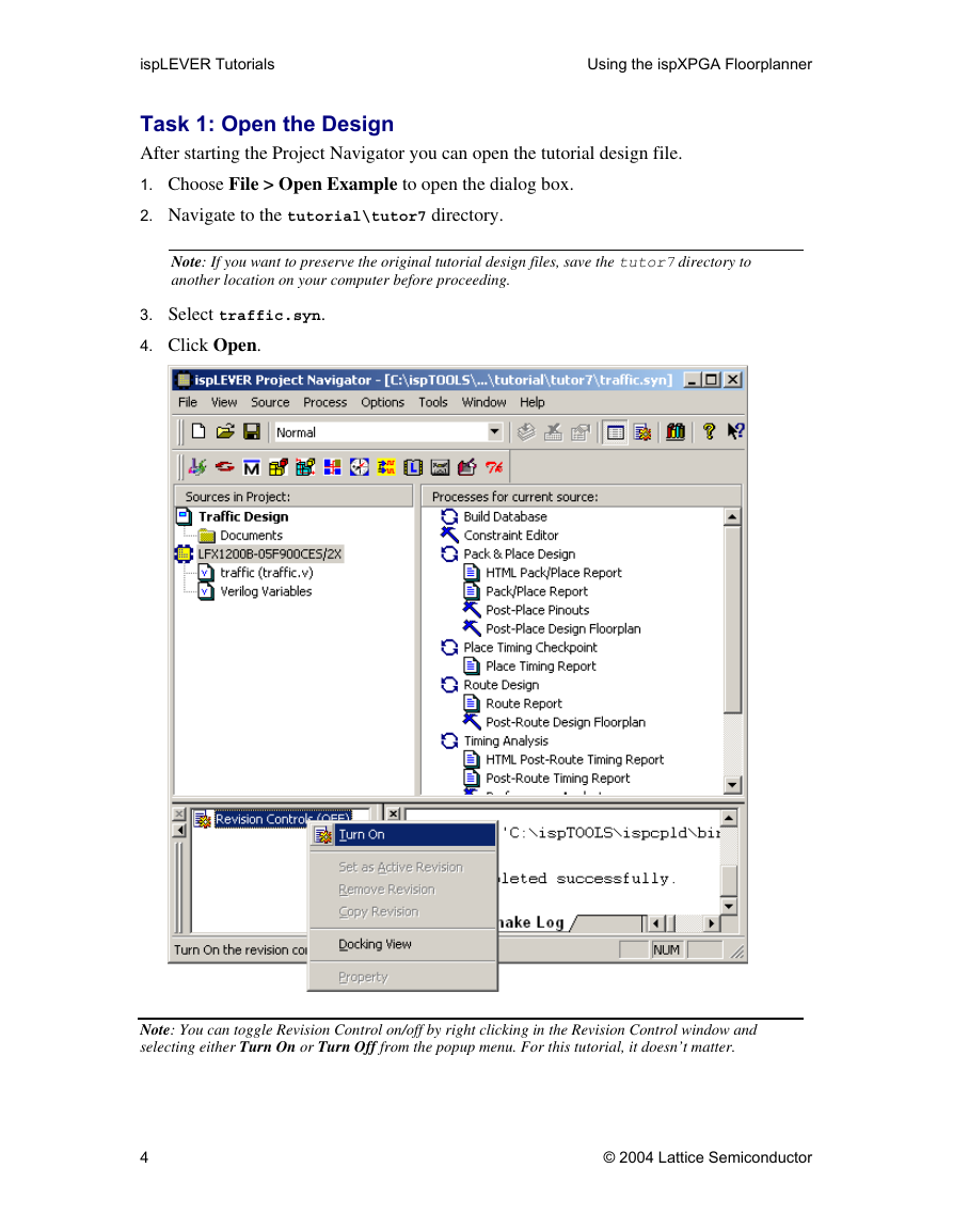
When you run the Post-Place Design Floorplan process, the project design
automatically loads into the Floorplanner.
To open a post-place design floorplan file:
•
In the Project Navigator Processes window, double-click the Post-Place Design
Floorplan process to open the Floorplanner with the current design. Your view will
look similar to this one.
© 2004 Lattice Semiconductor
5
�
ispLEVER Tutorials
Using the ispXPGA Floorplanner
Task 3: Tour the Graphical User Interface - The Design Browser
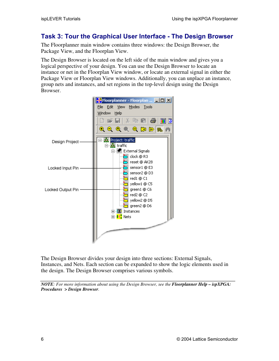
The Floorplanner main window contains three windows: the Design Browser, the
Package View, and the Floorplan View.
The Design Browser is located on the left side of the main window and gives you a
logical perspective of your design. You can use the Design Browser to locate an
instance or net in the Floorplan View window, or locate an external signal in either the
Package View or Floorplan View windows. Additionally, you can unplace an instance,
group nets and instances, and set regions in the top-level design using the Design
Browser.
The Design Browser divides your design into three sections: External Signals,
Instances, and Nets. Each section can be expanded to show the logic elements used in
the design. The Design Browser comprises various symbols.
NOTE: For more information about using the Design Browser, see the Floorplanner Help – ispXPGA:
Procedures > Design Browser.
6
© 2004 Lattice Semiconductor
�
ispLEVER Tutorials
Using the ispXPGA Floorplanner
Task 4: Tour the Graphical User Interface - The Package View
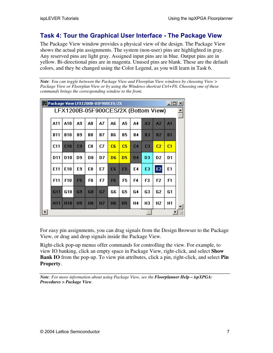
The Package View window provides a physical view of the design. The Package View
shows the actual pin assignments. The system (non-user) pins are highlighted in gray.
Any reserved pins are light gray. Assigned input pins are in blue. Output pins are in
yellow. Bi-directional pins are in magenta. Unused pins are blank. These are the default
colors, and they be changed using the Color Legend, as you will learn in Task 6.
Note: You can toggle between the Package View and Floorplan View windows by choosing View >
Package View or Floorplan View or by using the Windows shortcut Ctrl+F6. Choosing one of these
commands brings the corresponding window to the front.
For easy pin assignments, you can drag signals from the Design Browser to the Package
View, or drag and drop signals inside the Package View.
Right-click pop-up menus offer commands for controlling the view. For example, to
view IO banking, click an empty space in Package View, right-click, and select Show
Bank IO from the pop-up. To view pin attributes, click a pin, right-click, and select Pin
Property.
Note: For more information about using Package View, see the Floorplanner Help – ispXPGA:
Procedures > Package View.
© 2004 Lattice Semiconductor
7
�
ispLEVER Tutorials
Using the ispXPGA Floorplanner
Task 5: Tour the Graphical User Interface - The Floorplan View
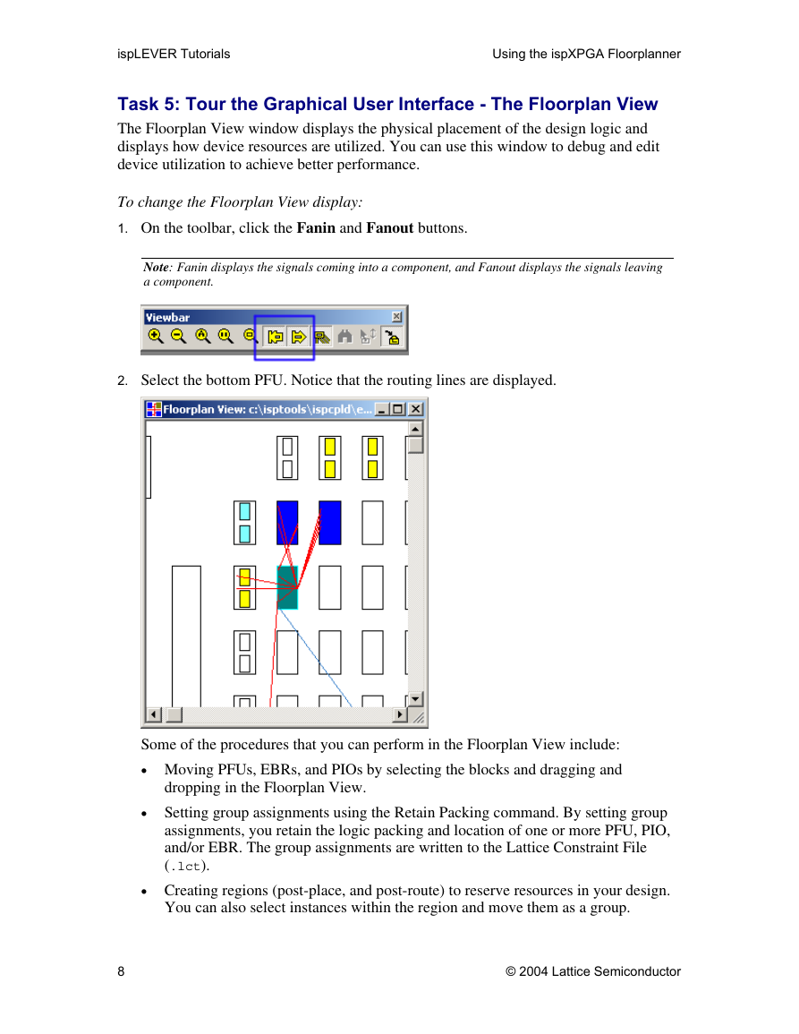
The Floorplan View window displays the physical placement of the design logic and
displays how device resources are utilized. You can use this window to debug and edit
device utilization to achieve better performance.
To change the Floorplan View display:
1. On the toolbar, click the Fanin and Fanout buttons.
Note: Fanin displays the signals coming into a component, and Fanout displays the signals leaving
a component.
2. Select the bottom PFU. Notice that the routing lines are displayed.
Some of the procedures that you can perform in the Floorplan View include:
• Moving PFUs, EBRs, and PIOs by selecting the blocks and dragging and
dropping in the Floorplan View.
• Setting group assignments using the Retain Packing command. By setting group
assignments, you retain the logic packing and location of one or more PFU, PIO,
and/or EBR. The group assignments are written to the Lattice Constraint File
(.lct).
• Creating regions (post-place, and post-route) to reserve resources in your design.
You can also select instances within the region and move them as a group.
8
© 2004 Lattice Semiconductor
�



 2023年江西萍乡中考道德与法治真题及答案.doc
 2012年重庆南川中考生物真题及答案.doc
 2013年江西师范大学地理学综合及文艺理论基础考研真题.doc
 2020年四川甘孜小升初语文真题及答案I卷.doc
 2020年注册岩土工程师专业基础考试真题及答案.doc
 2023-2024学年福建省厦门市九年级上学期数学月考试题及答案.doc
 2021-2022学年辽宁省沈阳市大东区九年级上学期语文期末试题及答案.doc
 2022-2023学年北京东城区初三第一学期物理期末试卷及答案.doc
 2018上半年江西教师资格初中地理学科知识与教学能力真题及答案.doc
 2012年河北国家公务员申论考试真题及答案-省级.doc
 2020-2021学年江苏省扬州市江都区邵樊片九年级上学期数学第一次质量检测试题及答案.doc
 2022下半年黑龙江教师资格证中学综合素质真题及答案.doc