A. Challenges in High Speed Serial Link Design
B. Signal Restoration using a Decision Feedback Equalizer (DFE)
Table of Contents
Setup
Introduction
Preliminaries
A. Opening Sue2 Schematics
B. Running CppSim Simulations
Plotting Time-Domain Results
A. Output signal plots
B. Output signal Eye Diagrams
C. RMS Jitter
Examining Non-Idealities
Behavioral Simulation of Decision Feedback
Equalizer Architectures Using CppSim
Matt Park and Michael Perrott
http://www-mtl.mit.edu/research/perrottgroup/
October 31, 2005
Copyright © 2005 by Matt Park and Michael Perrott
All rights reserved.
A. Intersymbol Interference (ISI)
B. Reflections
C. Non-Linearity and Offset
D. Gain-Bandwidth Limitations, Clock-to-Q Delays, and Metastability
DFE Calibration
DFE Architectures
A. Prototypical DFE
B. Half-Rate DFE with One-Tap of Speculation
I. Simulating and Analyzing Speculative Half-Rate Architecture in CppSim
Conclusion
Appendix: Generating Channel Impulse Response from Measured Data
Setup
Download and install the Cppsim package (i.e., download and run the self-extracting file
named setup_cppsim.exe) located at:
http://www-mtl.mit.edu/research/perrottgroup/tools.html
1
�
Upon completion of the installation, you will see icons on the Windows desktop
corresponding to the PLL Design Assistant, CppSimView, and Sue2. Please read the
“CppSim Primer” document, which is also at the same web address, to become
acquainted with CppSim and its various components.
Introduction
Most significant improvements in performance in increasingly complex communications
systems will arise from architectural innovations. These innovations are only possible
when you can quickly and accurately model and simulate the system under consideration.
CppSim, initially designed for simulating phase-locked loops, is a free behavioral
simulation package that leverages the C++ language to allow very fast simulation of a
wide array of system types. The goal of this tutorial is to expose the reader to a non-PLL
based system where modeling with CppSim enables the exploration of key design issues,
and may inspire new architectures for improved performance.
A. Challenges in High-Speed Serial Link Design
As IC technology continues to scale, multi-Gb/s data rates have become the norm in
many high-speed chips. This improvement in on-chip speed has led to a growing interest
in developing faster I/O for chip-to-chip communication. Unfortunately, the bandwidth
limitations of PCB and backplane traces and wires have not improved as dramatically
over the years, largely due to cost considerations. Consequently, channels that were
originally designed to support data rates in the 100 Mb/s realm are now being used to
transfer data in the 1-10 Gb/s range.
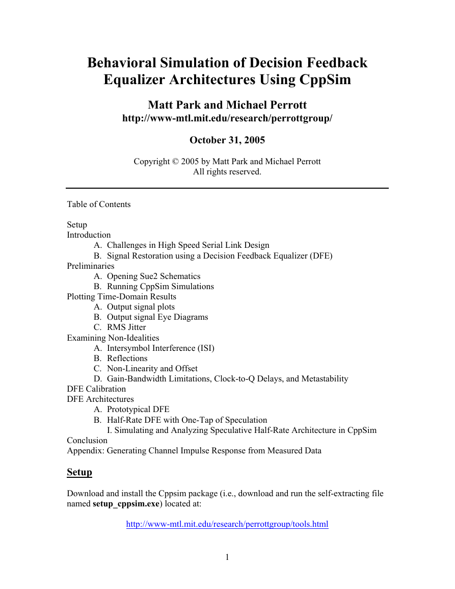
The frequency responses of two typical channels with different terminations are shown in
Figure 1. Notice the general low-pass characteristic of the channels caused by
capacitances and termination resistances, as well as skin effects and dielectric losses of
the PCB. Nulls in the response are due to resonances caused by impedance mismatches
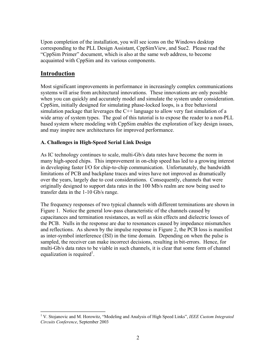
and reflections. As shown by the impulse response in Figure 2, the PCB loss is manifest
as inter-symbol interference (ISI) in the time domain. Depending on when the pulse is
sampled, the receiver can make incorrect decisions, resulting in bit-errors. Hence, for
multi-Gb/s data rates to be viable in such channels, it is clear that some form of channel
equalization is required1.
1 V. Stojanovic and M. Horowitz, “Modeling and Analysis of High Speed Links”, IEEE Custom Integrated
Circuits Conference, September 2003
2
�
Figure 1: frequency response of backplane channel1
Figure 2: pulse response of backplane channel1
B. Signal Restoration Using a Decision Feedback Equalizer (DFE)
Channel equalization can be accomplished through a number of techniques, such as high
pass filtering the data at the transmitter and/or receiver (a.k.a., feed-forward equalization
or FFE), and using tunable, impedance matching networks, just to name a few. The
merits and disadvantages of these approaches are discussed in2, and the reader is directed
there for more information.
This tutorial focuses on a particular form of equalization known as decision feedback
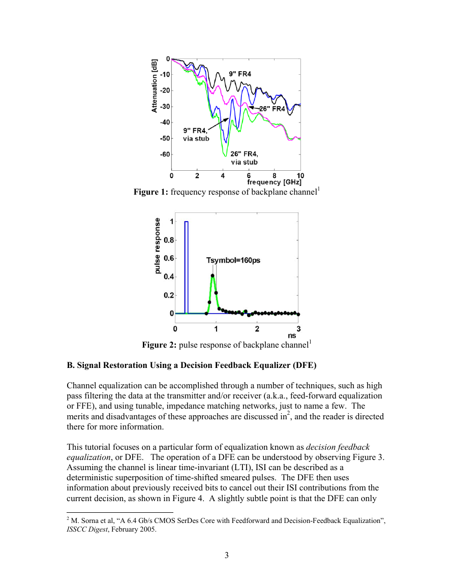
equalization, or DFE. The operation of a DFE can be understood by observing Figure 3.
Assuming the channel is linear time-invariant (LTI), ISI can be described as a
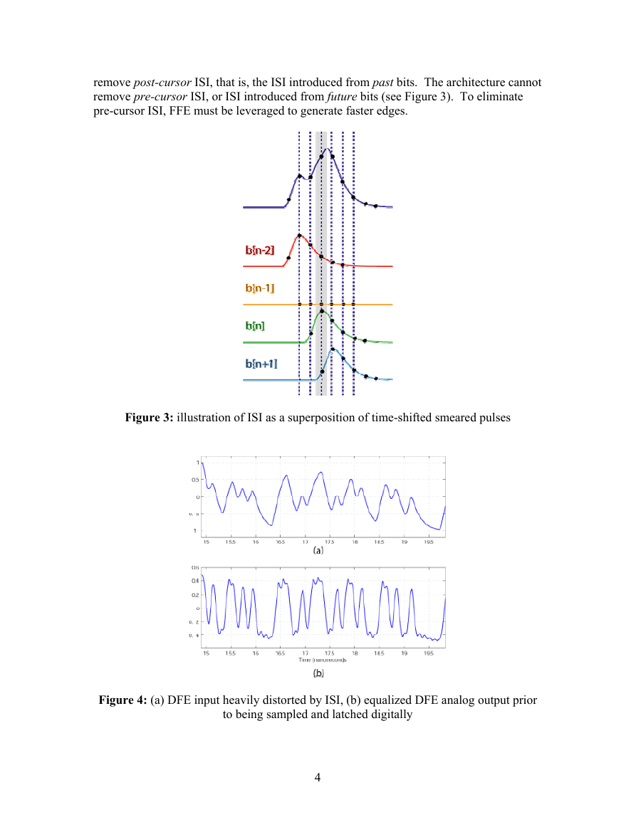
deterministic superposition of time-shifted smeared pulses. The DFE then uses
information about previously received bits to cancel out their ISI contributions from the
current decision, as shown in Figure 4. A slightly subtle point is that the DFE can only
2 M. Sorna et al, “A 6.4 Gb/s CMOS SerDes Core with Feedforward and Decision-Feedback Equalization”,
ISSCC Digest, February 2005.
3
�
remove post-cursor ISI, that is, the ISI introduced from past bits. The architecture cannot
remove pre-cursor ISI, or ISI introduced from future bits (see Figure 3). To eliminate
pre-cursor ISI, FFE must be leveraged to generate faster edges.
Figure 3: illustration of ISI as a superposition of time-shifted smeared pulses
Figure 4: (a) DFE input heavily distorted by ISI, (b) equalized DFE analog output prior
to being sampled and latched digitally
4
�
Preliminaries
A. Opening Sue2 Schematics
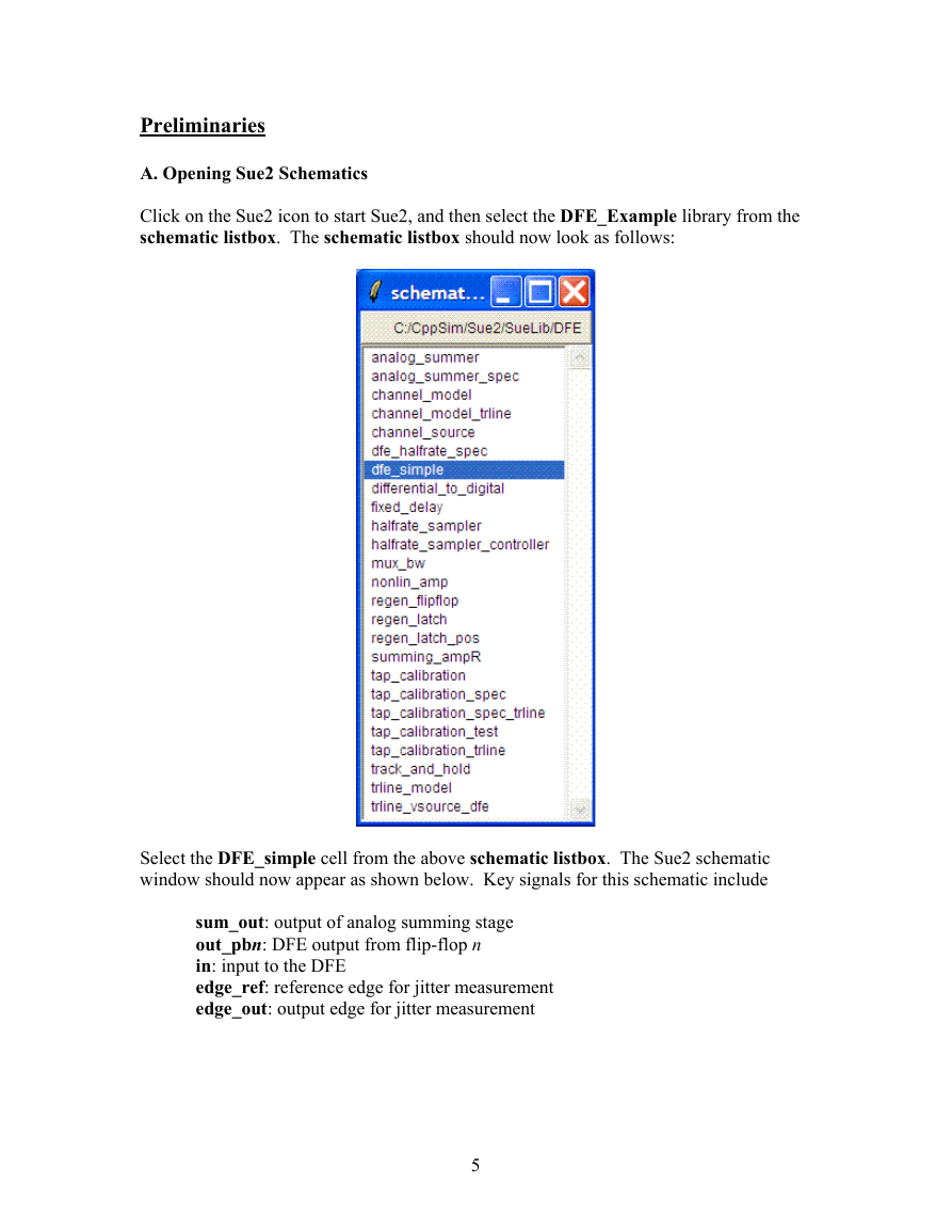
Click on the Sue2 icon to start Sue2, and then select the DFE_Example library from the
schematic listbox. The schematic listbox should now look as follows:
Select the DFE_simple cell from the above schematic listbox. The Sue2 schematic
window should now appear as shown below. Key signals for this schematic include
sum_out: output of analog summing stage
out_pbn: DFE output from flip-flop n
in: input to the DFE
edge_ref: reference edge for jitter measurement
edge_out: output edge for jitter measurement
5
�
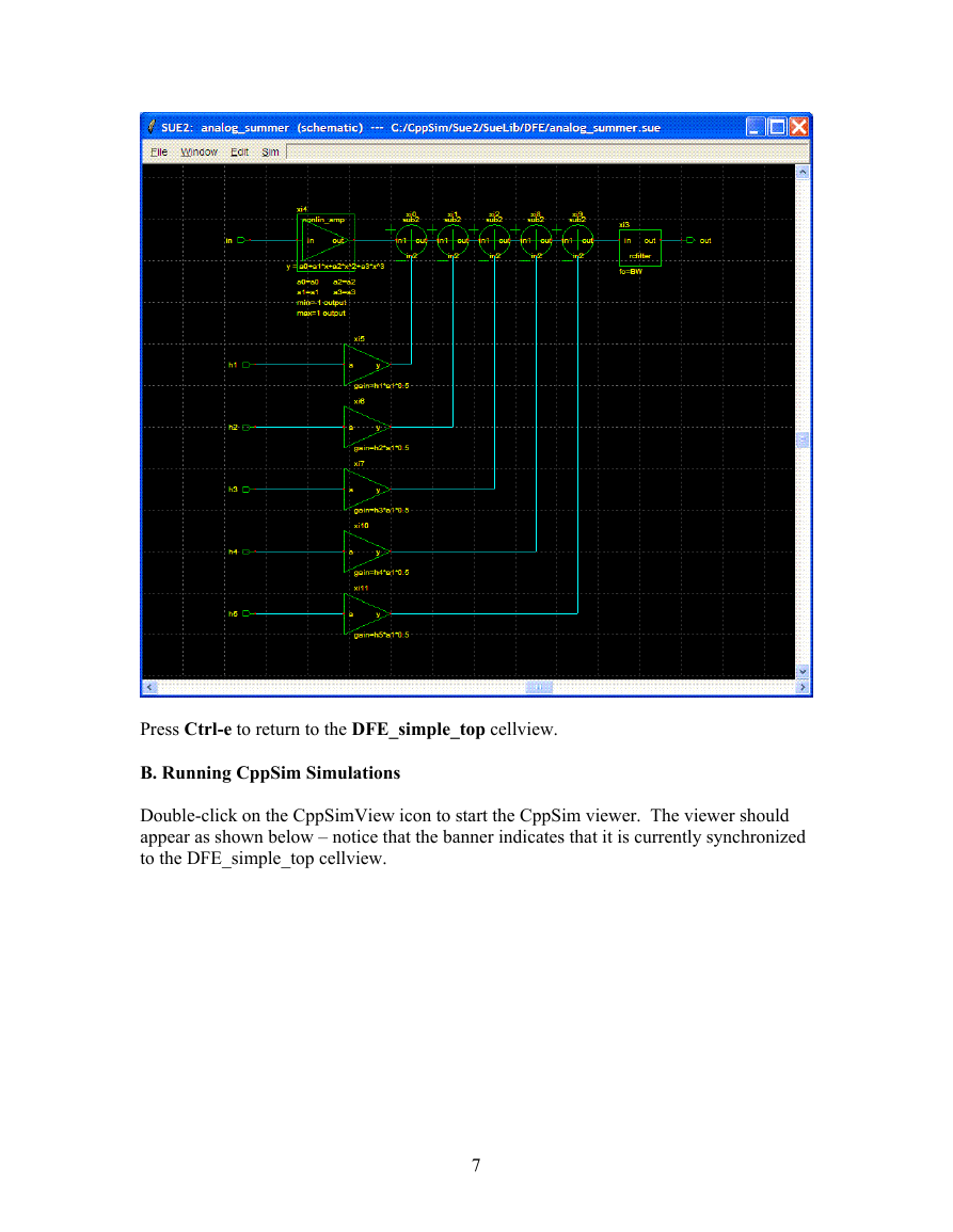
Select the analog_summer icon within the above schematic, and then press e to descend
down into the associated schematic. You should now see the schematic shown below.
6
�
Press Ctrl-e to return to the DFE_simple_top cellview.
B. Running CppSim Simulations
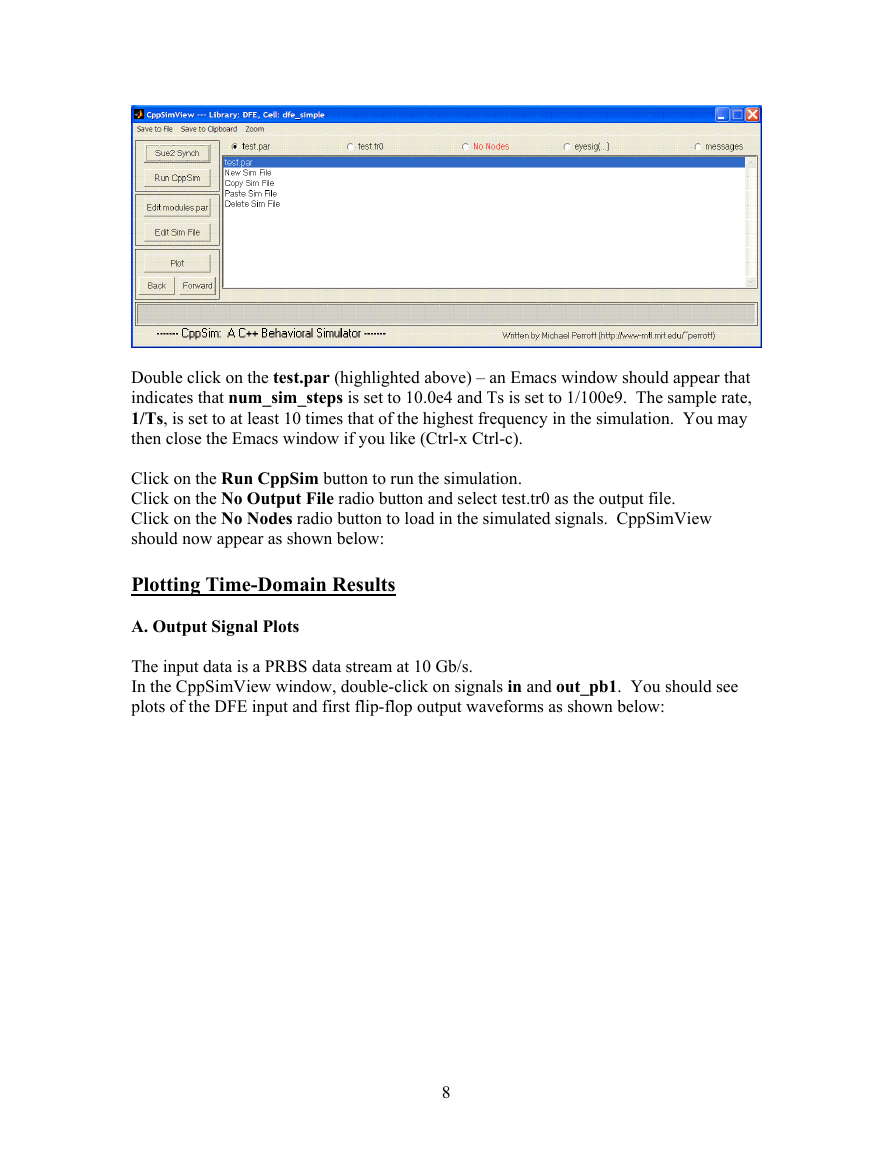
Double-click on the CppSimView icon to start the CppSim viewer. The viewer should
appear as shown below – notice that the banner indicates that it is currently synchronized
to the DFE_simple_top cellview.
7
�
Double click on the test.par (highlighted above) – an Emacs window should appear that
indicates that num_sim_steps is set to 10.0e4 and Ts is set to 1/100e9. The sample rate,
1/Ts, is set to at least 10 times that of the highest frequency in the simulation. You may
then close the Emacs window if you like (Ctrl-x Ctrl-c).
Click on the Run CppSim button to run the simulation.
Click on the No Output File radio button and select test.tr0 as the output file.
Click on the No Nodes radio button to load in the simulated signals. CppSimView
should now appear as shown below:
Plotting Time-Domain Results
A. Output Signal Plots
The input data is a PRBS data stream at 10 Gb/s.
In the CppSimView window, double-click on signals in and out_pb1. You should see
plots of the DFE input and first flip-flop output waveforms as shown below:
8
�



 2023年江西萍乡中考道德与法治真题及答案.doc
 2012年重庆南川中考生物真题及答案.doc
 2013年江西师范大学地理学综合及文艺理论基础考研真题.doc
 2020年四川甘孜小升初语文真题及答案I卷.doc
 2020年注册岩土工程师专业基础考试真题及答案.doc
 2023-2024学年福建省厦门市九年级上学期数学月考试题及答案.doc
 2021-2022学年辽宁省沈阳市大东区九年级上学期语文期末试题及答案.doc
 2022-2023学年北京东城区初三第一学期物理期末试卷及答案.doc
 2018上半年江西教师资格初中地理学科知识与教学能力真题及答案.doc
 2012年河北国家公务员申论考试真题及答案-省级.doc
 2020-2021学年江苏省扬州市江都区邵樊片九年级上学期数学第一次质量检测试题及答案.doc
 2022下半年黑龙江教师资格证中学综合素质真题及答案.doc