�
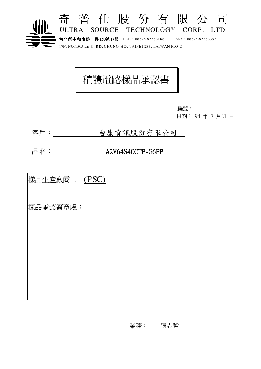
奇奇奇奇 普普普普 仕仕仕仕 股股股股 份份份份 有有有有 限限限限 公公公公 司司司司
ULTRA SOURCE TECHNOLOGY CORP. LTD.
台 北 縣 ㆗ 和 市 建 ㆒ 路 150150150150 號號號號 17171717 樓樓樓樓 TEL : 886-2-82263168 FAX : 886-2-82263353
台 北 縣 ㆗ 和 市 建 ㆒ 路
台 北 縣 ㆗ 和 市 建 ㆒ 路
台 北 縣 ㆗ 和 市 建 ㆒ 路
17F. NO.150Jian-Yi RD, CHUNG-HO, TAIPEI 235, TAIWAN R.O.C.
積體電路樣品承認書
`
.
編號:
日期: 94 年 7 月21 日
客戶:
A2V64S40CTP----G6PP
品名: A2V64S40CTP
G6PP
A2V64S40CTP
A2V64S40CTP
G6PP
G6PP
台康資訊股份有限公司
樣品生產廠商 : (PSC)
樣品承認簽章處:
業務: 陳志強
64Mb SDRAM Specification
A2V64S40CTP
No.12, Li-Hsin Rd.1, Science-based Industrial Park, Hsin-Chu
Taiwan, R.O.C.
TEL: 886-3-5795000
FAX: 886-3-5792168
�
Powerchip Semiconductor Corporation
A2V64S40CTP
64M Single Data Rate Synchronous DRAM
General Description
The A2V64S40CTP is 67,108,864 bits synchronous high data rate Dynamic RAM organized as 4 x 1,048,576 words by
16 bits. Synchronous design allows precise cycle controls with the use of system clock I/O transactions are possible on
every clock cycle. Range of operating frequencies, programmable burst length and programmable latencies allow the same
device to be useful for a variety of high bandwidth, high performance memory system applications.
Features
• 3.3V power supply
• LVTTL compatible with multiplexed address
• Four banks operation
• MRS cycle with address key programs
- CAS latency (2 & 3)
- Burst length (1, 2, 4, 8 & Full page)
- Burst type (Sequential & Interleave)
• All inputs are sampled at the positive going
edge of the system clock
• Auto & self refresh
• 64ms refresh period (4K cycle)
• Burst read single write operation
• LDQM & UDQM for masking
Ordering Information:
Pin Configurations
Package
400mil
TSOP-2
400mil
TSOP-2
400mil
TSOP-2
400mil
TSOP-2
Frequency Speed(ns)
Order Part Number
Type
Standard Pb-Free
200MHZ
166MHZ
143MHZ
133MHZ
5
6
7
A2V64S40CTP
A2V64S40CTP
A2V64S40CTP
-5
-6
-7
-G5
-G6
-G7
7.5
A2V64S40CTP
-75
-G75
Revision 1.0 Page 1/38 March, 2005
�
Powerchip Semiconductor Corporation
A2V64S40CTP
64M Single Data Rate Synchronous DRAM
DESCRIPTION
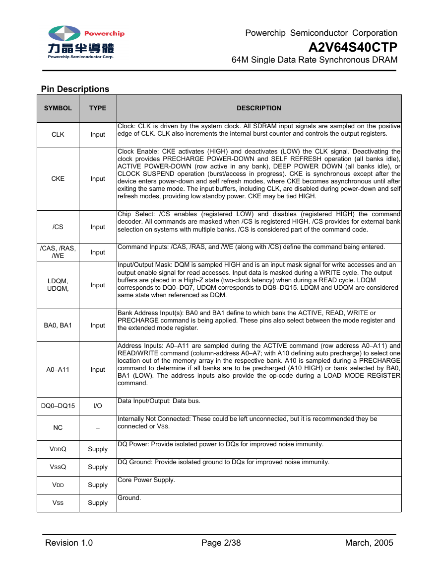
Clock: CLK is driven by the system clock. All SDRAM input signals are sampled on the positive
edge of CLK. CLK also increments the internal burst counter and controls the output registers.
Clock Enable: CKE activates (HIGH) and deactivates (LOW) the CLK signal. Deactivating the
clock provides PRECHARGE POWER-DOWN and SELF REFRESH operation (all banks idle),
ACTIVE POWER-DOWN (row active in any bank), DEEP POWER DOWN (all banks idle), or
CLOCK SUSPEND operation (burst/access in progress). CKE is synchronous except after the
device enters power-down and self refresh modes, where CKE becomes asynchronous until after
exiting the same mode. The input buffers, including CLK, are disabled during power-down and self
refresh modes, providing low standby power. CKE may be tied HIGH.
Chip Select: /CS enables (registered LOW) and disables (registered HIGH) the command
decoder. All commands are masked when /CS is registered HIGH. /CS provides for external bank
selection on systems with multiple banks. /CS is considered part of the command code.
Command Inputs: /CAS, /RAS, and /WE (along with /CS) define the command being entered.
Input/Output Mask: DQM is sampled HIGH and is an input mask signal for write accesses and an
output enable signal for read accesses. Input data is masked during a WRITE cycle. The output
buffers are placed in a High-Z state (two-clock latency) when during a READ cycle. LDQM
corresponds to DQ0–DQ7, UDQM corresponds to DQ8–DQ15. LDQM and UDQM are considered
same state when referenced as DQM.
Bank Address Input(s): BA0 and BA1 define to which bank the ACTIVE, READ, WRITE or
PRECHARGE command is being applied. These pins also select between the mode register and
the extended mode register.
Address Inputs: A0–A11 are sampled during the ACTIVE command (row address A0–A11) and
READ/WRITE command (column-address A0–A7; with A10 defining auto precharge) to select one
location out of the memory array in the respective bank. A10 is sampled during a PRECHARGE
command to determine if all banks are to be precharged (A10 HIGH) or bank selected by BA0,
BA1 (LOW). The address inputs also provide the op-code during a LOAD MODE REGISTER
command.
Data Input/Output: Data bus.
Internally Not Connected: These could be left unconnected, but it is recommended they be
connected or VSS.
Pin Descriptions
SYMBOL
TYPE
CLK
Input
CKE
Input
/CS
/CAS, /RAS,
/WE
LDQM,
UDQM,
Input
Input
Input
BA0, BA1
Input
A0–A11
Input
I/O
–
DQ0–DQ15
NC
VDDQ
VSSQ
VDD
VSS
Supply DQ Power: Provide isolated power to DQs for improved noise immunity.
Supply DQ Ground: Provide isolated ground to DQs for improved noise immunity.
Supply Core Power Supply.
Supply Ground.
Revision 1.0 Page 2/38 March, 2005
�
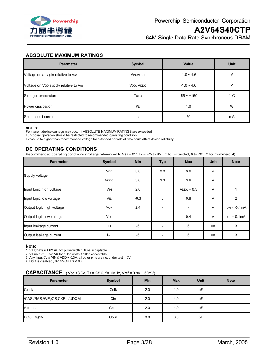
ABSOLUTE MAXIMUM RATINGS
Powerchip Semiconductor Corporation
A2V64S40CTP
64M Single Data Rate Synchronous DRAM
Unit
VIN,VOUT
Value
Symbol
VDD, VDDQ
Parameter
Voltage on any pin relative to Vss
Voltage on VDD supply relative to Vss
Storage temperature
Power dissipation
Short circuit current
NOTES:
Permanent device damage may occur if ABSOLUTE MAXIMUM RATINGS are exceeded.
Functional operation should be restricted to recommended operating condition.
Exposure to higher than recommended voltage for extended periods of time could affect device reliability.
DC OPERATING CONDITIONS
Recommended operating conditions (Voltage referenced to VSS = 0V, TA = -25 to 85° C for Extended, 0 to 70° C for Commercial)
-1.0 ~ 4.6
-1.0 ~ 4.6
-55 ~ +150
V
° C
W
mA
TSTG
PD
IOS
1.0
50
V
Parameter
Supply voltage
Symbol
VDD
VDDQ
Min
3.0
3.0
VIL
2.4
2.0
VIH
-0.3
VOH
Input logic high voltage
Input logic low voltage
Output logic high voltage
Output logic low voltage
Input leakage current
Output leakage current
Note:
1. VIH(max) = 4.6V AC for pulse width ≤ 10ns acceptable.
2. VIL(min) = -1.5V AC for pulse width ≤ 10ns acceptable.
3. Any input 0V ≤ VIN ≤ VDD + 0.3V, all other pins are not under test = 0V.
4. Dout is disabled , 0V ≤ VOUT ≤ VDD.
CAPACITANCE ( Vdd =3.3V, TA = 23°C, f = 1MHz, Vref = 0.9V ± 50mV)
VOL
IoL
ILI
-
-5
-5
Typ
3.3
3.3
0
-
-
-
-
Max
3.6
3.6
VDDQ + 0.3
0.8
-
0.4
5
5
Unit
Note
V
V
V
V
V
V
uA
uA
1
2
IOH = -0.1mA
IOL = 0.1mA
3
3
Parameter
Clock
/CAS,/RAS,/WE,/CS,CKE,L/UDQM
Address
DQ0~DQ15
Symbol
Cclk
Cin
CADD
COUT
Min
2.0
2.0
2.0
3.0
Max
4.0
4.0
4.0
6.0
Unit
pF
pF
pF
pF
Note
Revision 1.0 Page 3/38 March, 2005
�
Powerchip Semiconductor Corporation
A2V64S40CTP
64M Single Data Rate Synchronous DRAM
DC CHARACTERISTICS
Recommended operating conditions (Voltage referenced to VSS = 0V, TA = -25 to 85° C for Extended, 0 to 70° C for Commercial)
Parameter
Symbol
Test Condition
-5
Version
-6
-7
-75 Unit Note
Operating Current
(One Bank Active)
ICC1
Burst length = 1
tRC . tRC(min)
IO = 0 mA
120
110
100
95
mA
1
Precharge Standby Current in
power-down mode
ICC2P
CKE . VIL(max), tCC = 10ns
ICC2PS CKE & CLK . VIL(max), tCC = ∞
2
1
2
1
2
1
2
1
Precharge Standby Current
in non power-down mode
ICC2N
CKE . VIH(min), CS . VIH(min), tCC = 10ns
Input signals are changed one time during 20ns
20
20
20
20
ICC2NS CKE . VIH(min), CLK . VIL(max), tCC = ∞
Input signals are stable
Active Standby Current
in power-down mode
ICC3P
CKE . VIL(max), tCC = 10ns
ICC3PS CKE & CLK . VIL(max), tCC = ∞
15
10
10
15
10
10
15
10
10
15
10
10
Active Standby Current
in non power-down mode
(One Bank Active)
ICC3N
CKE . VIH(min), CS . VIH(min), tCC = 10ns
Input signals are changed one time during 20ns
30
30
30
30
ICC3NS CKE . VIH(min), CLK . VIL(max), tCC = ∞
Input signals are stable
25
25
25
25
mA
mA
mA
mA
160
150
140
130 mA
1
180
180
180
180 mA
1
1
1
1
mA
2
Operating Current
(Burst Mode)
ICC4
IO = 0 mA
Page burst
4Banks Activated
tCCD = 2CLKs
Refresh Current
ICC5
tARFC . tARFC(min)
ICC6
CKE . 0.2V
Self Refresh Current
NOTES:
1. Measured with outputs open.
2. Refresh period is 64ms.
3. Unless otherwise noted, input swing IeveI is CMOS(VIH /VIL=VDDQ/VSSQ).
Revision 1.0 Page 4/38 March, 2005
�
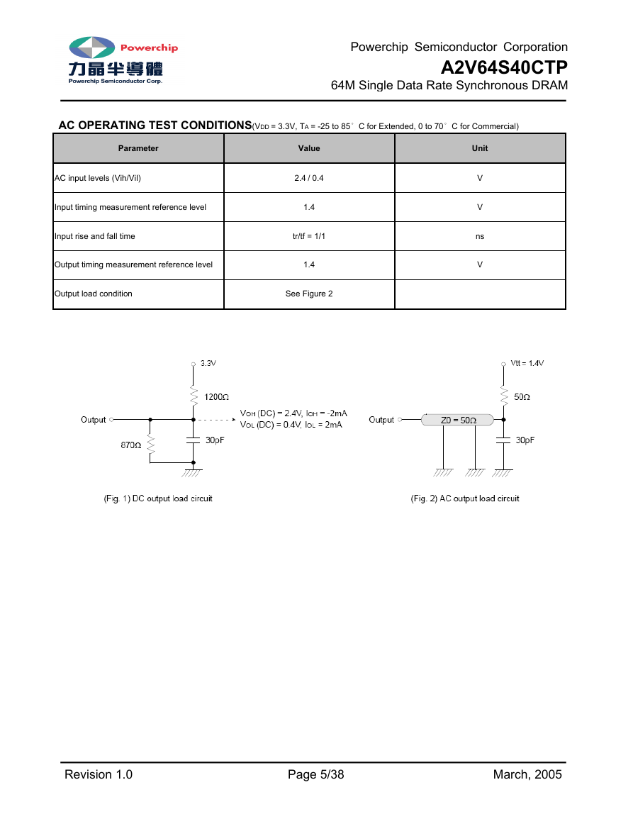
AC OPERATING TEST CONDITIONS(VDD = 3.3V, TA = -25 to 85° C for Extended, 0 to 70° C for Commercial)
Powerchip Semiconductor Corporation
A2V64S40CTP
64M Single Data Rate Synchronous DRAM
Parameter
AC input levels (Vih/Vil)
Input timing measurement reference level
Input rise and fall time
Output timing measurement reference level
Output load condition
Value
2.4 / 0.4
1.4
tr/tf = 1/1
1.4
See Figure 2
Unit
V
V
ns
V
Revision 1.0 Page 5/38 March, 2005
�




 2023年江西萍乡中考道德与法治真题及答案.doc
 2012年重庆南川中考生物真题及答案.doc
 2013年江西师范大学地理学综合及文艺理论基础考研真题.doc
 2020年四川甘孜小升初语文真题及答案I卷.doc
 2020年注册岩土工程师专业基础考试真题及答案.doc
 2023-2024学年福建省厦门市九年级上学期数学月考试题及答案.doc
 2021-2022学年辽宁省沈阳市大东区九年级上学期语文期末试题及答案.doc
 2022-2023学年北京东城区初三第一学期物理期末试卷及答案.doc
 2018上半年江西教师资格初中地理学科知识与教学能力真题及答案.doc
 2012年河北国家公务员申论考试真题及答案-省级.doc
 2020-2021学年江苏省扬州市江都区邵樊片九年级上学期数学第一次质量检测试题及答案.doc
 2022下半年黑龙江教师资格证中学综合素质真题及答案.doc