www.ti.com
ADS1294, ADS1294R
ADS1296, ADS1296R
ADS1298, ADS1298R
SBAS459H –JANUARY 2010–REVISED OCTOBER 2011
Low-Power, 8-Channel, 24-Bit Analog Front-End for Biopotential Measurements
Check for Samples: ADS1294, ADS1294R, ADS1296, ADS1296R, ADS1298, ADS1298R
1FEATURES
23• Eight Low-Noise PGAs and Eight
High-Resolution ADCs (ADS1298, ADS1298R)
Input-Referred Noise: 4μVPP (150Hz BW, G = 6)
Input Bias Current: 200pA
• Low Power: 0.75mW/channel
•
•
• Data Rate: 250SPS to 32kSPS
• CMRR: –115dB
• Programmable Gain: 1, 2, 3, 4, 6, 8, or 12
• Unipolar or Bipolar Supplies:
AVDD = 2.7V to 5.25V, DVDD = 1.65V to 3.6V
• Built-In Right Leg Drive Amplifier, Lead-Off
•
Detection, WCT, PACE Detection, Test Signals
Integrated Respiration Impedance
Measurement (ADS1294R/6R/8R only)
• Digital PACE Detection Capability
• Built-In Oscillator and Reference
• Flexible Power-Down, Standby Modes
• SPI™-Compatible Serial Interface
• Operating Temperature Range:
–40°C to +85°C
APPLICATIONS
• Medical Instrumentation (ECG, EMG and EEG):
Patient monitoring; Holter, event, stress, and
vital signs including ECG, AED, telemedicine
Bispectral index (BIS), Evoked audio potential
(EAP), Sleep study monitor
• High-Precision, Simultaneous, Multichannel
Signal Acquisition
the development of
integration and exceptional
With its high levels of
the ADS1294/6/8/4R/6R/8R family
performance,
enables
scalable medical
instrumentation systems at significantly reduced size,
power, and overall cost.
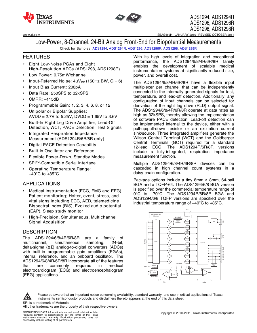
The ADS1294/6/8/4R/6R/8R have a flexible input
multiplexer per channel
that can be independently
connected to the internally-generated signals for test,
temperature, and lead-off detection. Additionally, any
configuration of input channels can be selected for
derivation of the right leg drive (RLD) output signal.
The ADS1294/6/8/4R/6R/8R operate at data rates as
high as 32kSPS, thereby allowing the implementation
of software PACE detection. Lead-off detection can
be implemented internal to the device, either with a
pull-up/pull-down resistor or an excitation current
sink/source. Three integrated amplifiers generate the
Wilson Central Terminal (WCT) and the Goldberger
Central Terminals (GCT)
required for a standard
12-lead ECG. The ADS1294R/6R/8R versions
include a fully-integrated,
respiration impedance
measurement function.
Multiple ADS1294/6/8/4R/6R/8R devices can be
cascaded in high channel count systems in a
daisy-chain configuration.
Package options include a tiny 8mm × 8mm, 64-ball
BGA and a TQFP-64. The ADS1294/6/8 BGA version
is specified over the commercial temperature range of
0°C to +70°C. The ADS1294R/6R/8R BGA and
ADS1294/6/8 TQFP versions are specified over the
industrial temperature range of –40°C to +85°C.
a
family
simultaneous
DESCRIPTION
of
The ADS1294/6/8/4R/6R/8R are
24-bit,
multichannel,
delta-sigma (ΔΣ) analog-to-digital converters (ADCs)
with built-in programmable gain amplifiers (PGAs),
internal reference, and an onboard oscillator. The
ADS1294/6/8/4R/6R/8R incorporate all of the features
that
medical
electrocardiogram (ECG) and electroencephalogram
(EEG) applications.
commonly
sampling,
are
required
in
1
Please be aware that an important notice concerning availability, standard warranty, and use in critical applications of Texas
Instruments semiconductor products and disclaimers thereto appears at the end of this data sheet.
2SPI is a trademark of Motorola.
3All other trademarks are the property of their respective owners.
PRODUCTION DATA information is current as of publication date.
Products conform to specifications per the terms of
the Texas
Instruments standard warranty. Production processing does not
necessarily include testing of all parameters.
Copyright © 2010–2011, Texas Instruments Incorporated
ControlCLKGPIO AND CONTROLOscillatorSPITest Signals andMonitorsPACESPIRLDWilsonTerminalWCTReferenceREFADC7ADC8ADC1ADC2ADC3ADC4ADC5ADC6A7A8A1A2A3A4A5A6MUXINPUTS¼¼¼To ChannelRESPRespRESPDEMODADS129xRADS129xR�
ADS1294, ADS1294R
ADS1296, ADS1296R
ADS1298, ADS1298R
SBAS459H –JANUARY 2010–REVISED OCTOBER 2011
www.ti.com
This integrated circuit can be damaged by ESD. Texas Instruments recommends that all
appropriate precautions. Failure to observe proper handling and installation procedures can cause damage.
integrated circuits be handled with
ESD damage can range from subtle performance degradation to complete device failure. Precision integrated circuits may be more
susceptible to damage because very small parametric changes could cause the device not to meet its published specifications.
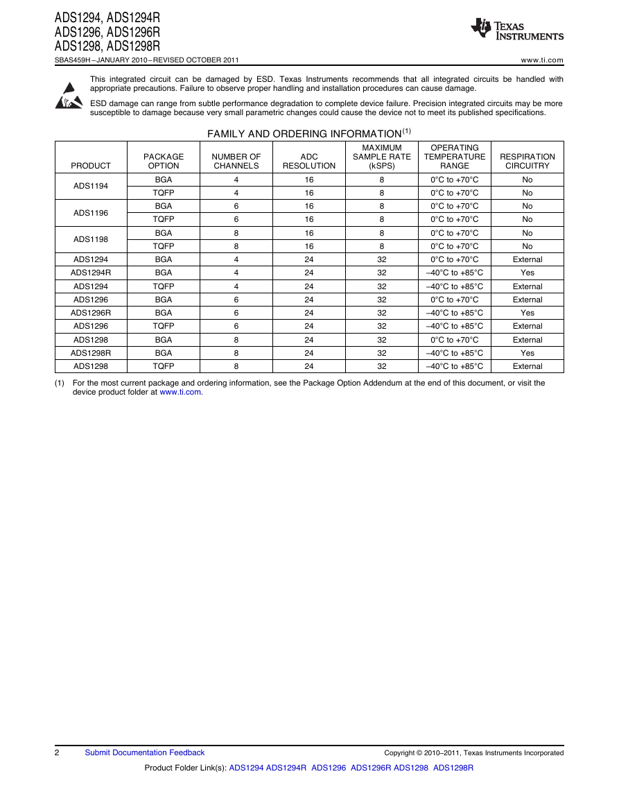
FAMILY AND ORDERING INFORMATION(1)
PRODUCT
ADS1194
ADS1196
ADS1198
ADS1294
ADS1294R
ADS1294
ADS1296
ADS1296R
ADS1296
ADS1298
ADS1298R
ADS1298
PACKAGE
OPTION
NUMBER OF
CHANNELS
ADC
RESOLUTION
MAXIMUM
SAMPLE RATE
(kSPS)
OPERATING
TEMPERATURE
RANGE
BGA
TQFP
BGA
TQFP
BGA
TQFP
BGA
BGA
TQFP
BGA
BGA
TQFP
BGA
BGA
TQFP
4
4
6
6
8
8
4
4
4
6
6
6
8
8
8
16
16
16
16
16
16
24
24
24
24
24
24
24
24
24
8
8
8
8
8
8
32
32
32
32
32
32
32
32
32
0°C to +70°C
0°C to +70°C
0°C to +70°C
0°C to +70°C
0°C to +70°C
0°C to +70°C
0°C to +70°C
–40°C to +85°C
–40°C to +85°C
0°C to +70°C
–40°C to +85°C
–40°C to +85°C
0°C to +70°C
–40°C to +85°C
–40°C to +85°C
RESPIRATION
CIRCUITRY
No
No
No
No
No
No
External
Yes
External
External
Yes
External
External
Yes
External
(1) For the most current package and ordering information, see the Package Option Addendum at the end of this document, or visit the
device product folder at www.ti.com.
2
Submit Documentation Feedback
Copyright © 2010–2011, Texas Instruments Incorporated
Product Folder Link(s): ADS1294 ADS1294R ADS1296 ADS1296R ADS1298 ADS1298R
�
www.ti.com
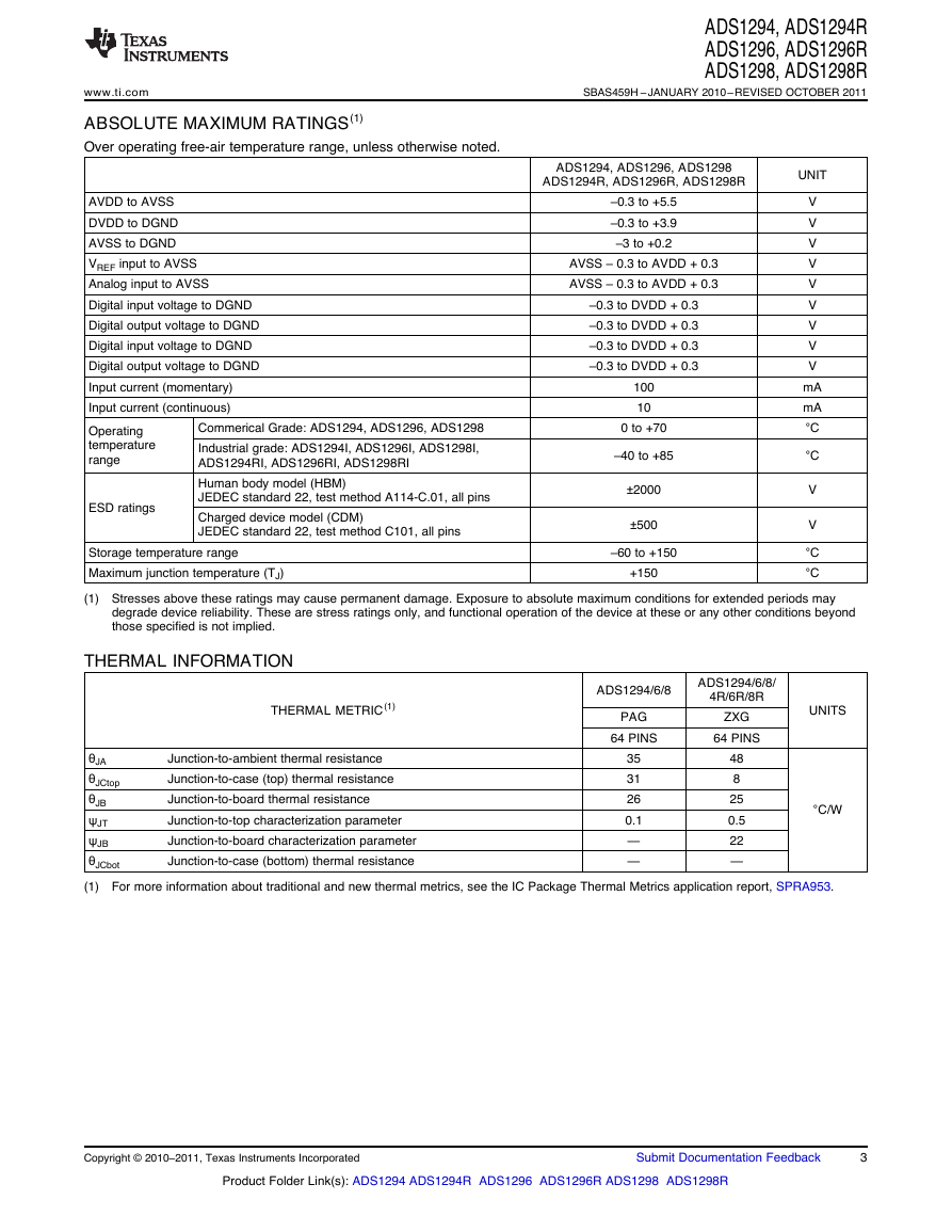
ABSOLUTE MAXIMUM RATINGS(1)
Over operating free-air temperature range, unless otherwise noted.
AVDD to AVSS
DVDD to DGND
AVSS to DGND
VREF input to AVSS
Analog input to AVSS
Digital input voltage to DGND
Digital output voltage to DGND
Digital input voltage to DGND
Digital output voltage to DGND
Input current (momentary)
Input current (continuous)
Operating
temperature
range
ESD ratings
Commerical Grade: ADS1294, ADS1296, ADS1298
Industrial grade: ADS1294I, ADS1296I, ADS1298I,
ADS1294RI, ADS1296RI, ADS1298RI
Human body model (HBM)
JEDEC standard 22, test method A114-C.01, all pins
Charged device model (CDM)
JEDEC standard 22, test method C101, all pins
Storage temperature range
Maximum junction temperature (TJ)
ADS1294, ADS1294R
ADS1296, ADS1296R
ADS1298, ADS1298R
SBAS459H –JANUARY 2010–REVISED OCTOBER 2011
ADS1294, ADS1296, ADS1298
ADS1294R, ADS1296R, ADS1298R
UNIT
–0.3 to +5.5
–0.3 to +3.9
–3 to +0.2
AVSS – 0.3 to AVDD + 0.3
AVSS – 0.3 to AVDD + 0.3
–0.3 to DVDD + 0.3
–0.3 to DVDD + 0.3
–0.3 to DVDD + 0.3
–0.3 to DVDD + 0.3
100
10
0 to +70
–40 to +85
±2000
±500
–60 to +150
+150
V
V
V
V
V
V
V
V
V
mA
mA
°C
°C
V
V
°C
°C
(1) Stresses above these ratings may cause permanent damage. Exposure to absolute maximum conditions for extended periods may
degrade device reliability. These are stress ratings only, and functional operation of the device at these or any other conditions beyond
those specified is not implied.
THERMAL INFORMATION
THERMAL METRIC(1)
θJA
θJCtop
θJB
ψJT
ψJB
θJCbot
Junction-to-ambient thermal resistance
Junction-to-case (top) thermal resistance
Junction-to-board thermal resistance
Junction-to-top characterization parameter
Junction-to-board characterization parameter
Junction-to-case (bottom) thermal resistance
ADS1294/6/8
PAG
64 PINS
ADS1294/6/8/
4R/6R/8R
ZXG
64 PINS
35
31
26
0.1
—
—
48
8
25
0.5
22
—
UNITS
°C/W
(1) For more information about traditional and new thermal metrics, see the IC Package Thermal Metrics application report, SPRA953.
Copyright © 2010–2011, Texas Instruments Incorporated
Submit Documentation Feedback
3
Product Folder Link(s): ADS1294 ADS1294R ADS1296 ADS1296R ADS1298 ADS1298R
�
ADS1294, ADS1294R
ADS1296, ADS1296R
ADS1298, ADS1298R
SBAS459H –JANUARY 2010–REVISED OCTOBER 2011
www.ti.com
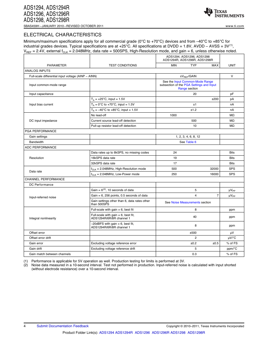
ELECTRICAL CHARACTERISTICS
Minimum/maximum specifications apply for all commercial grade (0°C to +70°C) devices and from –40°C to +85°C for
industrial grades devices. Typical specifications are at +25°C. All specifications at DVDD = 1.8V, AVDD – AVSS = 3V (1),
VREF = 2.4V, external fCLK = 2.048MHz, data rate = 500SPS, High-Resolution mode, and gain = 6, unless otherwise noted.
PARAMETER
TEST CONDITIONS
MIN
TYP
MAX
UNIT
ADS1294, ADS1296, ADS1298
ADS1294R, ADS1296R, ADS1298R
ANALOG INPUTS
Full-scale differential input voltage (AINP – AINN)
±VREF/GAIN
V
pF
pA
nA
nA
MΩ
MΩ
MΩ
Bits
Bits
Bits
SPS
SPS
μVPP
μVPP
ppm
ppm
ppm
µV
32000
16000
7
5
4
See Noise Measurements section
8
40
8
±500
2
±0.2
5
0.3
±0.5
µV/°C
% of FS
ppm/°C
% of FS
Input common-mode range
Input capacitance
Input bias current
DC input impedance
PGA PERFORMANCE
Gain settings
Bandwidth
ADC PERFORMANCE
Resolution
Data rate
CHANNEL PERFORMANCE
DC Performance
Input-referred noise
Integral nonlinearity
Offset error
Offset error drift
Gain error
Gain drift
Gain match between channels
See the Input Common-Mode Range
subsection of the PGA Settings and Input
Range section
TA = +25°C, input = 1.5V
TA = 0°C to +70°C, input = 1.5V
TA = –40°C to +85°C, input = 1.5V
No lead-off
Current source lead-off detection
Pull-up resistor lead-off detection
±200
20
±1
±1.2
500
10
1000
1, 2, 3, 4, 6, 8, 12
See Table 6
Data rates up to 8kSPS, no missing codes
16kSPS data rate
32kSPS data rate
fCLK = 2.048MHz, High-Resolution mode
fCLK = 2.048MHz, Low-Power mode
24
19
17
500
250
Gain = 6 (2), 10 seconds of data
Gain = 6, 256 points, 0.5 seconds of data
Gain settings other than 6, data rates other
than 500SPS
Full-scale with gain = 6, best fit
Full-scale with gain = 6, best fit,
ADS1294R/6R/8R channel 1
–20dBFS with gain = 6, best fit,
ADS1294R/6R/8R channel 1
Excluding voltage reference error
Excluding voltage reference drift
(1) Performance is applicable for 5V operation as well. Production testing for limits is performed at 3V.
(2) Noise data measured in a 10-second interval. Test not performed in production. Input-referred noise is calculated with input shorted
(without electrode resistance) over a 10-second interval.
4
Submit Documentation Feedback
Copyright © 2010–2011, Texas Instruments Incorporated
Product Folder Link(s): ADS1294 ADS1294R ADS1296 ADS1296R ADS1298 ADS1298R
�
www.ti.com
ADS1294, ADS1294R
ADS1296, ADS1296R
ADS1298, ADS1298R
SBAS459H –JANUARY 2010–REVISED OCTOBER 2011
ELECTRICAL CHARACTERISTICS (continued)
Minimum/maximum specifications apply for all commercial grade (0°C to +70°C) devices and from –40°C to +85°C for
industrial grades devices. Typical specifications are at +25°C. All specifications at DVDD = 1.8V, AVDD – AVSS = 3V(1),
VREF = 2.4V, external fCLK = 2.048MHz, data rate = 500SPS, High-Resolution mode, and gain = 6, unless otherwise noted.
PARAMETER
TEST CONDITIONS
MIN
TYP
MAX
UNIT
ADS1294, ADS1296, ADS1298
ADS1294R, ADS1296R, ADS1298R
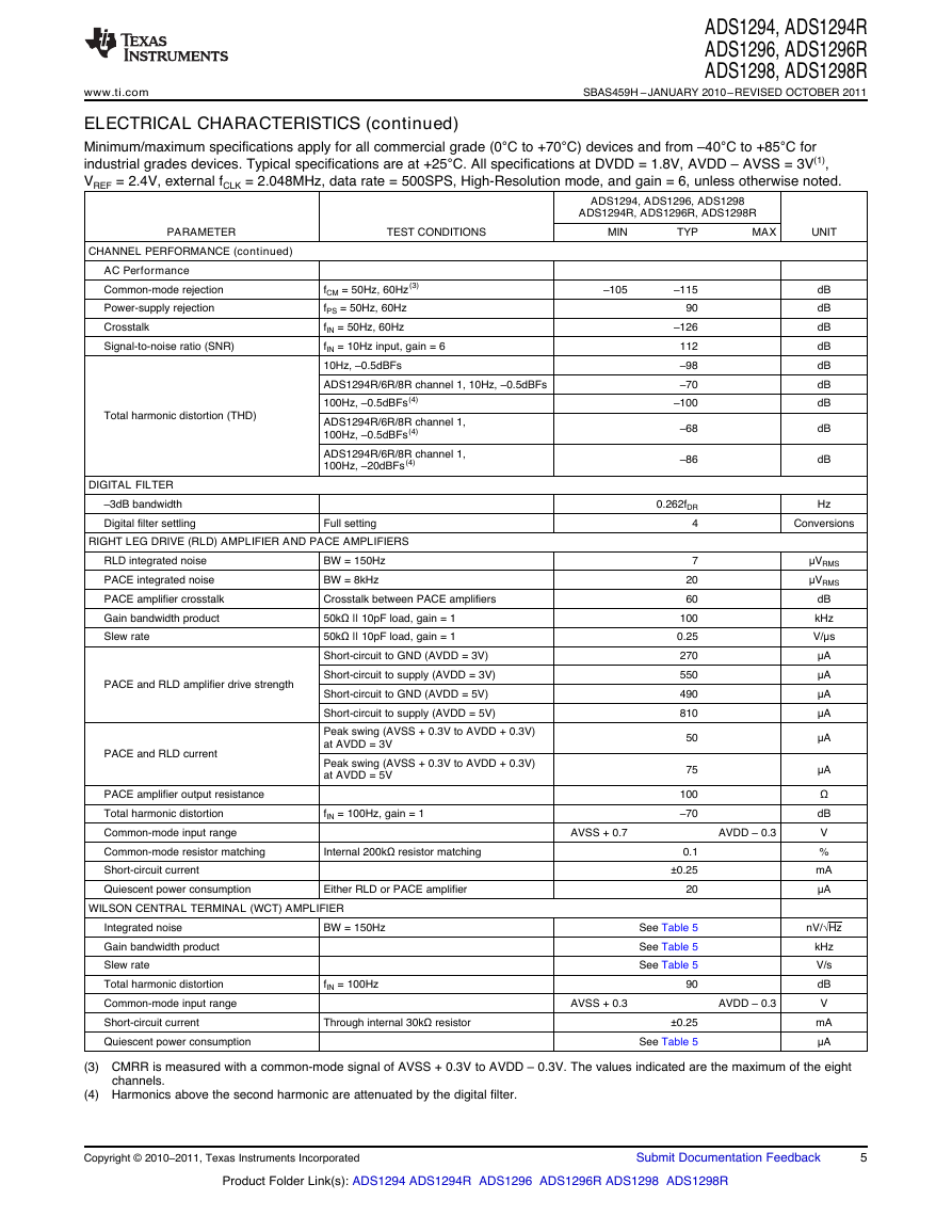
CHANNEL PERFORMANCE (continued)
AC Performance
Common-mode rejection
Power-supply rejection
Crosstalk
Signal-to-noise ratio (SNR)
Total harmonic distortion (THD)
–105
fCM = 50Hz, 60Hz (3)
fPS = 50Hz, 60Hz
fIN = 50Hz, 60Hz
fIN = 10Hz input, gain = 6
10Hz, –0.5dBFs
ADS1294R/6R/8R channel 1, 10Hz, –0.5dBFs
100Hz, –0.5dBFs (4)
ADS1294R/6R/8R channel 1,
100Hz, –0.5dBFs(4)
ADS1294R/6R/8R channel 1,
100Hz, –20dBFs (4)
DIGITAL FILTER
–3dB bandwidth
Digital filter settling
Full setting
RIGHT LEG DRIVE (RLD) AMPLIFIER AND PACE AMPLIFIERS
RLD integrated noise
PACE integrated noise
PACE amplifier crosstalk
Gain bandwidth product
Slew rate
PACE and RLD amplifier drive strength
PACE and RLD current
PACE amplifier output resistance
Total harmonic distortion
Common-mode input range
BW = 150Hz
BW = 8kHz
Crosstalk between PACE amplifiers
50kΩ || 10pF load, gain = 1
50kΩ || 10pF load, gain = 1
Short-circuit to GND (AVDD = 3V)
Short-circuit to supply (AVDD = 3V)
Short-circuit to GND (AVDD = 5V)
Short-circuit to supply (AVDD = 5V)
Peak swing (AVSS + 0.3V to AVDD + 0.3V)
at AVDD = 3V
Peak swing (AVSS + 0.3V to AVDD + 0.3V)
at AVDD = 5V
fIN = 100Hz, gain = 1
Common-mode resistor matching
Internal 200kΩ resistor matching
Short-circuit current
Quiescent power consumption
Either RLD or PACE amplifier
WILSON CENTRAL TERMINAL (WCT) AMPLIFIER
–115
90
–126
112
–98
–70
–100
–68
–86
0.262fDR
4
7
20
60
100
0.25
270
550
490
810
50
75
100
–70
dB
dB
dB
dB
dB
dB
dB
dB
dB
Hz
Conversions
μVRMS
µVRMS
dB
kHz
V/μs
μA
μA
μA
μA
μA
μA
Ω
dB
V
%
mA
μA
nV/√Hz
kHz
V/s
dB
V
mA
μA
AVSS + 0.7
AVDD – 0.3
0.1
±0.25
20
See Table 5
See Table 5
See Table 5
90
±0.25
See Table 5
AVDD – 0.3
Integrated noise
Gain bandwidth product
Slew rate
Total harmonic distortion
Common-mode input range
Short-circuit current
Quiescent power consumption
BW = 150Hz
fIN = 100Hz
Through internal 30kΩ resistor
AVSS + 0.3
(3) CMRR is measured with a common-mode signal of AVSS + 0.3V to AVDD – 0.3V. The values indicated are the maximum of the eight
channels.
(4) Harmonics above the second harmonic are attenuated by the digital filter.
Copyright © 2010–2011, Texas Instruments Incorporated
Submit Documentation Feedback
5
Product Folder Link(s): ADS1294 ADS1294R ADS1296 ADS1296R ADS1298 ADS1298R
�
ADS1294, ADS1294R
ADS1296, ADS1296R
ADS1298, ADS1298R
SBAS459H –JANUARY 2010–REVISED OCTOBER 2011
www.ti.com
ELECTRICAL CHARACTERISTICS (continued)
Minimum/maximum specifications apply for all commercial grade (0°C to +70°C) devices and from –40°C to +85°C for
industrial grades devices. Typical specifications are at +25°C. All specifications at DVDD = 1.8V, AVDD – AVSS = 3V(1),
VREF = 2.4V, external fCLK = 2.048MHz, data rate = 500SPS, High-Resolution mode, and gain = 6, unless otherwise noted.
PARAMETER
TEST CONDITIONS
MIN
TYP
MAX
UNIT
ADS1294, ADS1296, ADS1298
ADS1294R, ADS1296R, ADS1298R
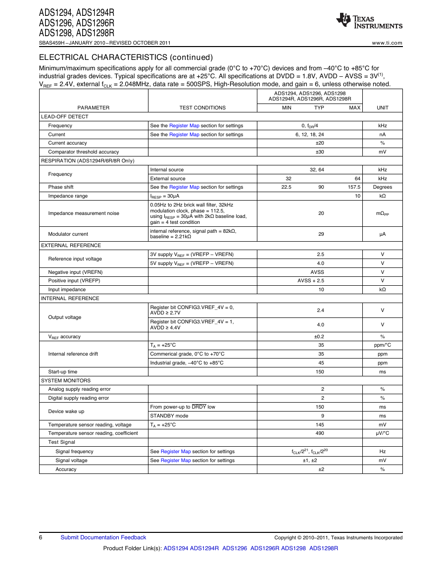
LEAD-OFF DETECT
Frequency
Current
Current accuracy
Comparator threshold accuracy
RESPIRATION (ADS1294R/6R/8R Only)
Frequency
Phase shift
Impedance range
Impedance measurement noise
Modulator current
EXTERNAL REFERENCE
Reference input voltage
Negative input (VREFN)
Positive input (VREFP)
Input impedance
INTERNAL REFERENCE
Output voltage
VREF accuracy
Internal reference drift
Start-up time
SYSTEM MONITORS
Analog supply reading error
Digital supply reading error
Device wake up
Temperature sensor reading, voltage
Temperature sensor reading, coefficient
Test Signal
Signal frequency
Signal voltage
Accuracy
See the Register Map section for settings
See the Register Map section for settings
Internal source
External source
See the Register Map section for settings
IRESP = 30μA
0.05Hz to 2Hz brick wall filter, 32kHz
modulation clock, phase = 112.5,
using IRESP = 30μA with 2kΩ baseline load,
gain = 4 test condition
internal reference, signal path = 82kΩ,
baseline = 2.21kΩ
3V supply VREF = (VREFP – VREFN)
5V supply VREF = (VREFP – VREFN)
Register bit CONFIG3.VREF_4V = 0,
AVDD ≥ 2.7V
Register bit CONFIG3.VREF_4V = 1,
AVDD ≥ 4.4V
TA = +25°C
Commerical grade, 0°C to +70°C
Industrial grade, –40°C to +85°C
From power-up to DRDY low
STANDBY mode
TA = +25°C
32
22.5
0, fDR/4
6, 12, 18, 24
±20
±30
32, 64
90
20
29
2.5
4.0
AVSS
AVSS + 2.5
10
2.4
4.0
±0.2
35
35
45
150
2
2
150
9
145
490
See Register Map section for settings
See Register Map section for settings
fCLK/221, fCLK/220
±1, ±2
±2
kHz
nA
%
mV
kHz
kHz
64
157.5
Degrees
10
kΩ
mΩPP
µA
V
V
V
V
kΩ
V
V
%
ppm/°C
ppm
ppm
ms
%
%
ms
ms
mV
μV/°C
Hz
mV
%
6
Submit Documentation Feedback
Copyright © 2010–2011, Texas Instruments Incorporated
Product Folder Link(s): ADS1294 ADS1294R ADS1296 ADS1296R ADS1298 ADS1298R
�
www.ti.com
ADS1294, ADS1294R
ADS1296, ADS1296R
ADS1298, ADS1298R
SBAS459H –JANUARY 2010–REVISED OCTOBER 2011
ELECTRICAL CHARACTERISTICS (continued)
Minimum/maximum specifications apply for all commercial grade (0°C to +70°C) devices and from –40°C to +85°C for
industrial grades devices. Typical specifications are at +25°C. All specifications at DVDD = 1.8V, AVDD – AVSS = 3V(1),
VREF = 2.4V, external fCLK = 2.048MHz, data rate = 500SPS, High-Resolution mode, and gain = 6, unless otherwise noted.
PARAMETER
TEST CONDITIONS
MIN
TYP
MAX
UNIT
ADS1294, ADS1296, ADS1298
ADS1294R, ADS1296R, ADS1298R
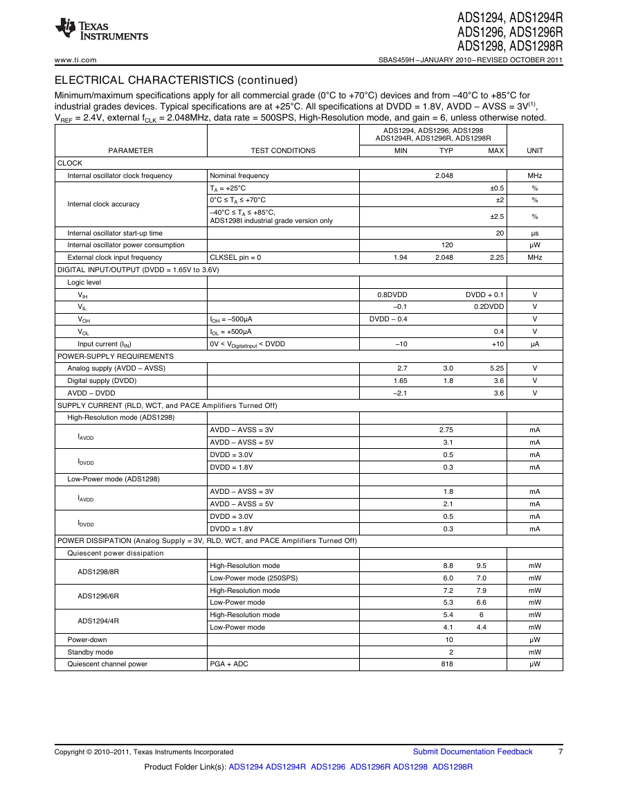
CLOCK
Internal oscillator clock frequency
Internal clock accuracy
Nominal frequency
TA = +25°C
0°C ≤ TA ≤ +70°C
–40°C ≤ TA ≤ +85°C,
ADS1298I industrial grade version only
Internal oscillator start-up time
Internal oscillator power consumption
External clock input frequency
CLKSEL pin = 0
DIGITAL INPUT/OUTPUT (DVDD = 1.65V to 3.6V)
2.048
1.94
120
2.048
0.8DVDD
–0.1
DVDD – 0.4
–10
2.7
1.65
–2.1
Logic level
VIH
VIL
VOH
VOL
Input current (IIN)
POWER-SUPPLY REQUIREMENTS
Analog supply (AVDD – AVSS)
Digital supply (DVDD)
AVDD – DVDD
IOH = –500μA
IOL = +500μA
0V < VDigitalInput < DVDD
SUPPLY CURRENT (RLD, WCT, and PACE Amplifiers Turned Off)
High-Resolution mode (ADS1298)
IAVDD
IDVDD
Low-Power mode (ADS1298)
IAVDD
IDVDD
AVDD – AVSS = 3V
AVDD – AVSS = 5V
DVDD = 3.0V
DVDD = 1.8V
AVDD – AVSS = 3V
AVDD – AVSS = 5V
DVDD = 3.0V
DVDD = 1.8V
POWER DISSIPATION (Analog Supply = 3V, RLD, WCT, and PACE Amplifiers Turned Off)
Quiescent power dissipation
ADS1298/8R
ADS1296/6R
ADS1294/4R
Power-down
Standby mode
High-Resolution mode
Low-Power mode (250SPS)
High-Resolution mode
Low-Power mode
High-Resolution mode
Low-Power mode
Quiescent channel power
PGA + ADC
3.0
1.8
2.75
3.1
0.5
0.3
1.8
2.1
0.5
0.3
8.8
6.0
7.2
5.3
5.4
4.1
10
2
818
±0.5
±2
±2.5
20
2.25
DVDD + 0.1
0.2DVDD
0.4
+10
5.25
3.6
3.6
9.5
7.0
7.9
6.6
6
4.4
MHz
%
%
%
μs
μW
MHz
V
V
V
V
μA
V
V
V
mA
mA
mA
mA
mA
mA
mA
mA
mW
mW
mW
mW
mW
mW
μW
mW
μW
Copyright © 2010–2011, Texas Instruments Incorporated
Submit Documentation Feedback
7
Product Folder Link(s): ADS1294 ADS1294R ADS1296 ADS1296R ADS1298 ADS1298R
�
ADS1294, ADS1294R
ADS1296, ADS1296R
ADS1298, ADS1298R
SBAS459H –JANUARY 2010–REVISED OCTOBER 2011
www.ti.com
ELECTRICAL CHARACTERISTICS (continued)
Minimum/maximum specifications apply for all commercial grade (0°C to +70°C) devices and from –40°C to +85°C for
industrial grades devices. Typical specifications are at +25°C. All specifications at DVDD = 1.8V, AVDD – AVSS = 3V(1),
VREF = 2.4V, external fCLK = 2.048MHz, data rate = 500SPS, High-Resolution mode, and gain = 6, unless otherwise noted.
ADS1294, ADS1296, ADS1298
ADS1294R, ADS1296R, ADS1298R
PARAMETER
TEST CONDITIONS
MIN
TYP
MAX
UNIT
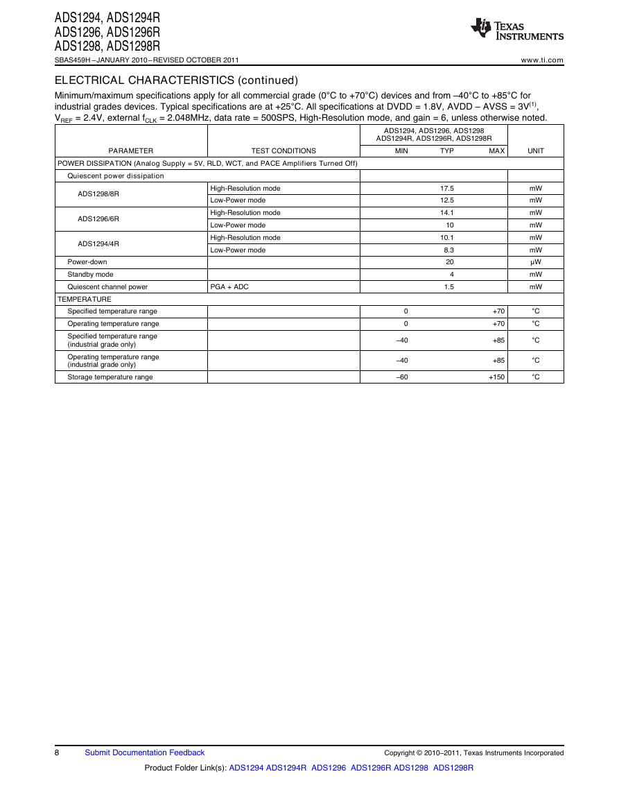
POWER DISSIPATION (Analog Supply = 5V, RLD, WCT, and PACE Amplifiers Turned Off)
Quiescent power dissipation
ADS1298/8R
ADS1296/6R
ADS1294/4R
Power-down
Standby mode
High-Resolution mode
Low-Power mode
High-Resolution mode
Low-Power mode
High-Resolution mode
Low-Power mode
Quiescent channel power
PGA + ADC
TEMPERATURE
Specified temperature range
Operating temperature range
Specified temperature range
(industrial grade only)
Operating temperature range
(industrial grade only)
Storage temperature range
17.5
12.5
14.1
10
10.1
8.3
20
4
1.5
0
0
–40
–40
–60
+70
+70
+85
+85
+150
mW
mW
mW
mW
mW
mW
μW
mW
mW
°C
°C
°C
°C
°C
8
Submit Documentation Feedback
Copyright © 2010–2011, Texas Instruments Incorporated
Product Folder Link(s): ADS1294 ADS1294R ADS1296 ADS1296R ADS1298 ADS1298R
�


 2023年江西萍乡中考道德与法治真题及答案.doc
 2012年重庆南川中考生物真题及答案.doc
 2013年江西师范大学地理学综合及文艺理论基础考研真题.doc
 2020年四川甘孜小升初语文真题及答案I卷.doc
 2020年注册岩土工程师专业基础考试真题及答案.doc
 2023-2024学年福建省厦门市九年级上学期数学月考试题及答案.doc
 2021-2022学年辽宁省沈阳市大东区九年级上学期语文期末试题及答案.doc
 2022-2023学年北京东城区初三第一学期物理期末试卷及答案.doc
 2018上半年江西教师资格初中地理学科知识与教学能力真题及答案.doc
 2012年河北国家公务员申论考试真题及答案-省级.doc
 2020-2021学年江苏省扬州市江都区邵樊片九年级上学期数学第一次质量检测试题及答案.doc
 2022下半年黑龙江教师资格证中学综合素质真题及答案.doc