ACT8846
Rev 5, 09-Mar-17
Advanced PMU for Multi-core Application Processors
GENERAL DESCRIPTION
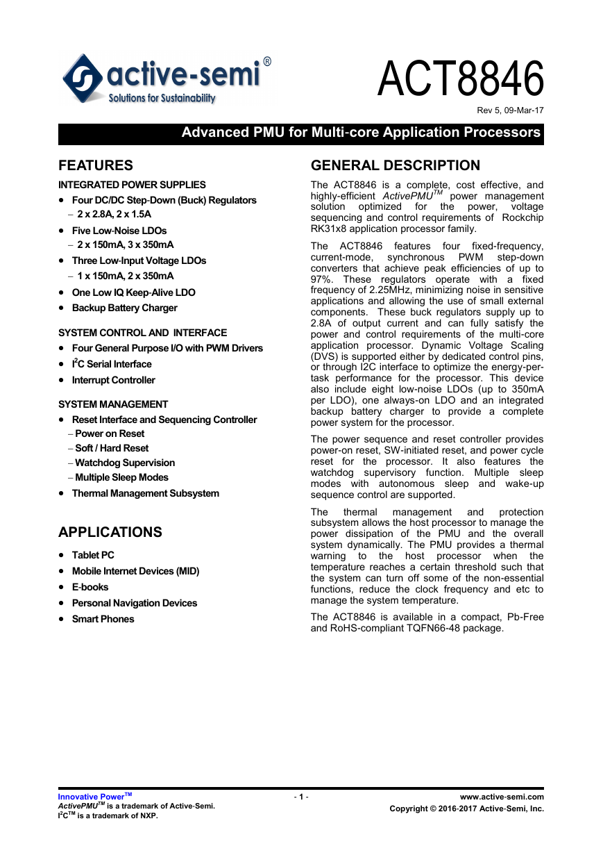
The ACT8846 is a complete, cost effective, and
highly-efficient ActivePMUTM power management
solution optimized
voltage
sequencing and control requirements of Rockchip
RK31x8 application processor family.
the power,
for
four
features
synchronous PWM
regulators operate with a
fixed-frequency,
The ACT8846
current-mode,
step-down
converters that achieve peak efficiencies of up to
97%. These
fixed
frequency of 2.25MHz, minimizing noise in sensitive
applications and allowing the use of small external
components. These buck regulators supply up to
2.8A of output current and can fully satisfy the
power and control requirements of the multi-core
application processor. Dynamic Voltage Scaling
(DVS) is supported either by dedicated control pins,
or through I2C interface to optimize the energy-per-
task performance for the processor. This device
also include eight low-noise LDOs (up to 350mA
per LDO), one always-on LDO and an integrated
backup battery charger to provide a complete
power system for the processor.
for
The power sequence and reset controller provides
power-on reset, SW-initiated reset, and power cycle
reset
the
watchdog supervisory
function. Multiple sleep
modes with autonomous sleep and wake-up
sequence control are supported.
the processor.
features
It also
and
thermal management
The
protection
subsystem allows the host processor to manage the
power dissipation of the PMU and the overall
system dynamically. The PMU provides a thermal
warning
the
temperature reaches a certain threshold such that
the system can turn off some of the non-essential
functions, reduce the clock frequency and etc to
manage the system temperature.
the host processor when
to
The ACT8846 is available in a compact, Pb-Free
and RoHS-compliant TQFN66-48 package.
FEATURES
INTEGRATED POWER SUPPLIES
Four DC/DC Step-Down (Buck) Regulators
2 x 2.8A, 2 x 1.5A
Five Low-Noise LDOs
2 x 150mA, 3 x 350mA
Three Low-Input Voltage LDOs
1 x 150mA, 2 x 350mA
One Low IQ Keep-Alive LDO
Backup Battery Charger
SYSTEM CONTROL AND INTERFACE
Four General Purpose I/O with PWM Drivers
I2C Serial Interface
Interrupt Controller
SYSTEM MANAGEMENT
Reset Interface and Sequencing Controller
Power on Reset
Soft / Hard Reset
Watchdog Supervision
Multiple Sleep Modes
Thermal Management Subsystem
APPLICATIONS
Tablet PC
Mobile Internet Devices (MID)
E-books
Personal Navigation Devices
Smart Phones
Innovative PowerTM
ActivePMUTM is a trademark of Active-Semi.
I2CTM is a trademark of NXP.
- 1 -
www.active-semi.com
Copyright © 2016-2017 Active-Semi, Inc.
�
FUNCTIONAL BLOCK DIAGRAM
ACT8846
Rev 5, 09-Mar-17
Innovative PowerTM
ActivePMUTM is a trademark of Active-Semi.
I2CTM is a trademark of NXP.
- 2 -
www.active-semi.com
Copyright © 2016-2017 Active-Semi, Inc.
SDAREG2VP2GP2SW2OUT2OUT2REG1VP1GP14SW1OUT1FB1To BatterynIRQREG5LDOOUT5OUT5INL1REFBPReferenceREG3VP3GP3SW3OUT3OUT3GAEPnPBSTATPWRHLDPWRENSCLnRSTOVSELR2VIOnPBINPUSH BUTTONINL2REG6LDOOUT6OUT6REG7LDOOUT7OUT7REG10LDOOUT10OUT10To BatteryTo BatteryREG4VP4GP14SW4OUT4OUT4To BatteryREG11LDOOUT11OUT11INL3REG12LDOOUT12OUT12VIOVIOREG13RTC LDOOUT13GPIO2GPIO1GPIO3SystemControlINL2REG8LDOOUT8OUT8REG9LDOOUT9OUT9OUT13ACT8846To BatteryTo BatteryTo BatteryGPIO4GPIO6GPIO5�
ORDERING INFORMATION
ACT8846
Rev 5, 09-Mar-17
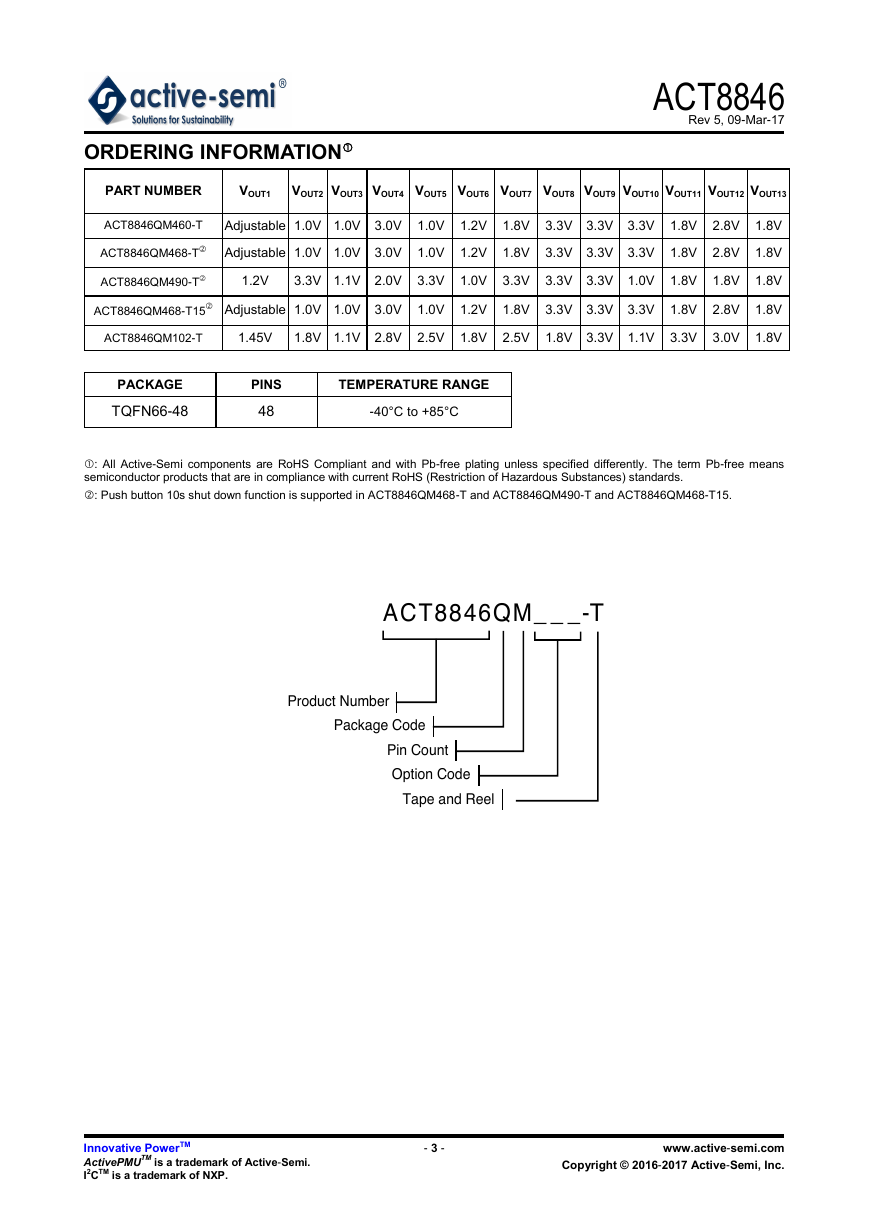
PART NUMBER
VOUT1 VOUT2 VOUT3 VOUT4 VOUT5 VOUT6 VOUT7 VOUT8 VOUT9 VOUT10 VOUT11 VOUT12 VOUT13
ACT8846QM460-T
Adjustable 1.0V 1.0V 3.0V 1.0V 1.2V 1.8V 3.3V 3.3V 3.3V 1.8V 2.8V 1.8V
ACT8846QM468-T
Adjustable 1.0V 1.0V 3.0V 1.0V 1.2V 1.8V 3.3V 3.3V 3.3V 1.8V 2.8V 1.8V
ACT8846QM490-T
1.2V
3.3V 1.1V 2.0V 3.3V 1.0V 3.3V 3.3V 3.3V 1.0V 1.8V 1.8V 1.8V
ACT8846QM468-T15
Adjustable 1.0V 1.0V 3.0V 1.0V 1.2V 1.8V 3.3V 3.3V 3.3V 1.8V 2.8V 1.8V
ACT8846QM102-T
1.45V
1.8V 1.1V 2.8V 2.5V 1.8V 2.5V 1.8V 3.3V 1.1V 3.3V 3.0V 1.8V
PACKAGE
TQFN66-48
PINS
48
TEMPERATURE RANGE
-40°C to +85°C
: All Active-Semi components are RoHS Compliant and with Pb-free plating unless specified differently. The term Pb-free means
semiconductor products that are in compliance with current RoHS (Restriction of Hazardous Substances) standards.
: Push button 10s shut down function is supported in ACT8846QM468-T and ACT8846QM490-T and ACT8846QM468-T15.
Innovative PowerTM
ActivePMUTM is a trademark of Active-Semi.
I2CTM is a trademark of NXP.
- 3 -
www.active-semi.com
Copyright © 2016-2017 Active-Semi, Inc.
ACT8846QM_ _ _-TOption CodePin CountPackage CodeProduct NumberTape and Reel�
ACT8846
Rev 5, 09-Mar-17
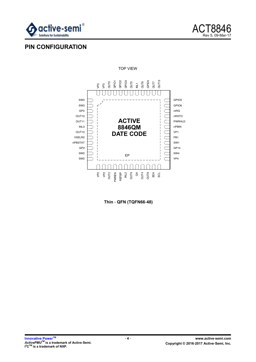
PIN CONFIGURATION
TOP VIEW
ACTIVE
8846QM
DATE CODE
Thin - QFN (TQFN66-48)
Innovative PowerTM
ActivePMUTM is a trademark of Active-Semi.
I2CTM is a trademark of NXP.
- 4 -
www.active-semi.com
Copyright © 2016-2017 Active-Semi, Inc.
EPOUT13OUT7GPIO4OUT6INL1OUT5GPIO3GPIO2GPIO1OUT3GPIO5GPIO6nIRQnRSTOPWRHLDnPBINVP1FB1SW1GP14SW3SW3GP3OUT10OUT11INL3OUT12VSELR2nPBSTATGP2SCLSDAOUT4GAOUT9INL2REFBPPWRENOUT2OUT8VP3VP3SW2SW2VP2VP2SW4VP4�
PIN DESCRIPTIONS
ACT8846
Rev 5, 09-Mar-17
PIN
1, 2
3
4
5
6
7
8
9
NAME
DESCRIPTION
SW3
Switch Node for REG3.
GP3
Power Ground for REG3. Connect GP14, GP2, GP3, and GA together at a single
point as close to the IC as possible.
OUT10
REG10 output. Bypass it to ground with a 2.2µF capacitor.
OUT11
REG11 output. Bypass it to ground with a 2.2µF capacitor.
INL3
Power input for REG10, REG11 and REG12.
OUT12
REG12 output. Bypass it to ground with a 2.2µF capacitor.
VSELR2
Output Voltage Selection for REG2. Drive to logic low to select default output voltage.
Drive to logic high to select secondary output voltage.
nPBSTAT
Active-Low Open-Drain Push-Button Status Output. nPBSTAT is asserted low
whenever the nPBIN is pushed, and is high-Z otherwise.
10
GP2
Power ground for REG2. Connect GP14, GP2, GP3, and GA together at a single
point as close to the IC as possible.
11, 12
SW2
Switch Node for REG2.
13, 14
VP2
Power input for REG2. Bypass to GP2 with a high quality ceramic capacitor placed as
close to the IC as possible.
15
16
17
18
19
20
21
22
23
24
25
OUT2
Output Voltage Sense for REG2.
PWREN
Power Enable Input for REG3. PWREN is functional only when PWRHLD is driven
high. Drive PWREN to a logic high to turn on the REG3. Drive PWREN to a logic low
to turn off the REG3.
REFBP
Reference Bypass. Connect a 0.047μF ceramic capacitor from REFBP to GA. This
pin is discharged to GA in shutdown.
INL2
Power Input for REG8, REG9.
OUT9
REG9 output. Bypass it to ground with a 2.2µF capacitor.
GA
Analog Ground.
OUT4
Output voltage sense for REG4.
OUT8
REG8 output. Bypass it to ground with a 2.2µF capacitor.
SDA
Data Input for I2C Serial Interface. Data is read on the rising edge of SCL.
SCL
Clock Input for I2C Serial Interface.
VP4
Power input for REG4. Bypass to GP14 with a high quality ceramic capacitor placed
as close to the IC as possible.
Innovative PowerTM
ActivePMUTM is a trademark of Active-Semi.
I2CTM is a trademark of NXP.
- 5 -
www.active-semi.com
Copyright © 2016-2017 Active-Semi, Inc.
�
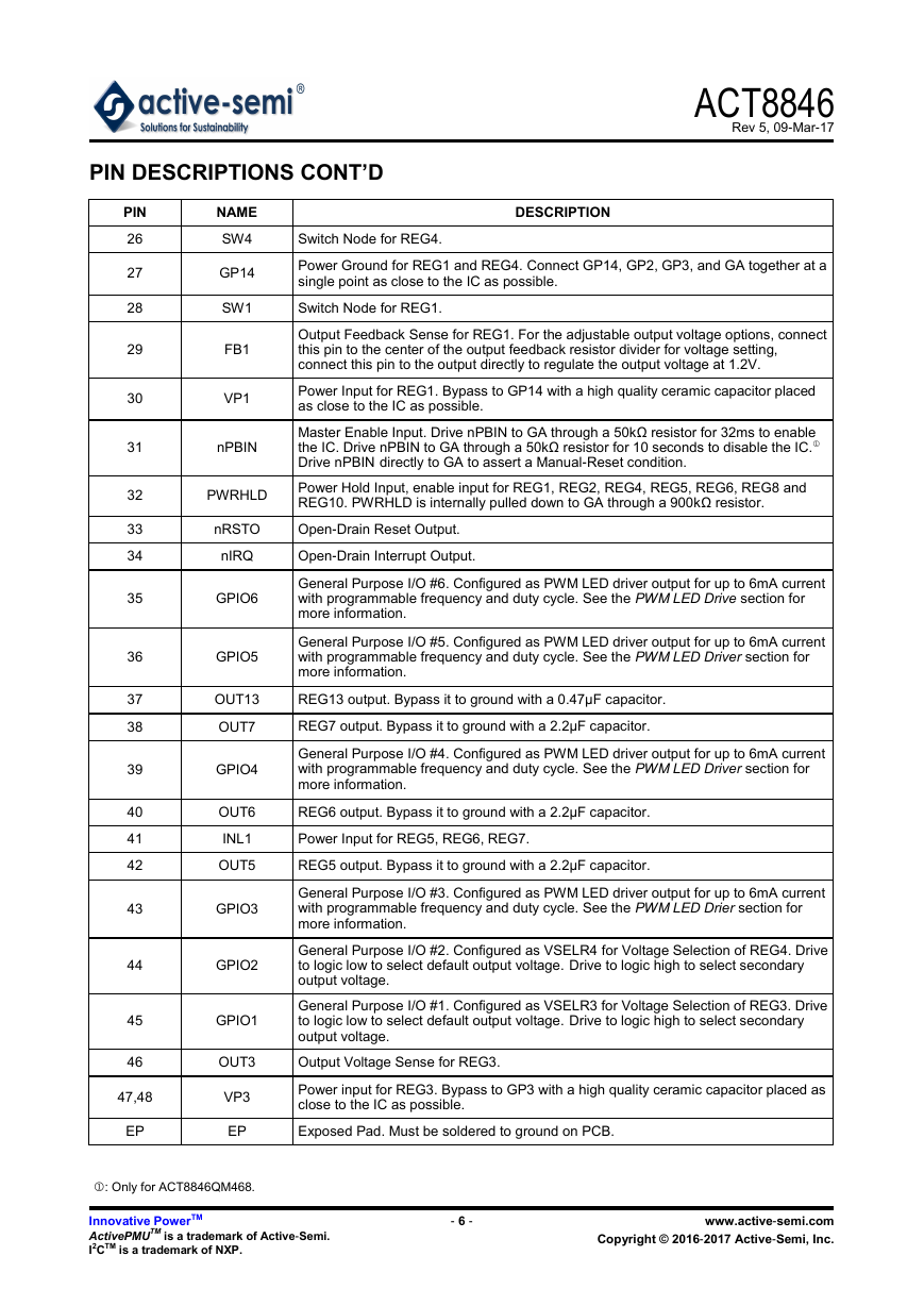
PIN DESCRIPTIONS CONT’D
ACT8846
Rev 5, 09-Mar-17
PIN
26
27
28
29
30
31
32
33
34
35
36
37
38
39
40
41
42
43
44
45
46
NAME
SW4
GP14
Switch Node for REG4.
DESCRIPTION
Power Ground for REG1 and REG4. Connect GP14, GP2, GP3, and GA together at a
single point as close to the IC as possible.
SW1
Switch Node for REG1.
FB1
VP1
nPBIN
Output Feedback Sense for REG1. For the adjustable output voltage options, connect
this pin to the center of the output feedback resistor divider for voltage setting,
connect this pin to the output directly to regulate the output voltage at 1.2V.
Power Input for REG1. Bypass to GP14 with a high quality ceramic capacitor placed
as close to the IC as possible.
Master Enable Input. Drive nPBIN to GA through a 50kΩ resistor for 32ms to enable
the IC. Drive nPBIN to GA through a 50kΩ resistor for 10 seconds to disable the IC.
Drive nPBIN directly to GA to assert a Manual-Reset condition.
PWRHLD
Power Hold Input, enable input for REG1, REG2, REG4, REG5, REG6, REG8 and
REG10. PWRHLD is internally pulled down to GA through a 900kΩ resistor.
nRSTO
Open-Drain Reset Output.
nIRQ
Open-Drain Interrupt Output.
GPIO6
GPIO5
OUT13
OUT7
GPIO4
OUT6
INL1
OUT5
GPIO3
GPIO2
GPIO1
General Purpose I/O #6. Configured as PWM LED driver output for up to 6mA current
with programmable frequency and duty cycle. See the PWM LED Drive section for
more information.
General Purpose I/O #5. Configured as PWM LED driver output for up to 6mA current
with programmable frequency and duty cycle. See the PWM LED Driver section for
more information.
REG13 output. Bypass it to ground with a 0.47µF capacitor.
REG7 output. Bypass it to ground with a 2.2µF capacitor.
General Purpose I/O #4. Configured as PWM LED driver output for up to 6mA current
with programmable frequency and duty cycle. See the PWM LED Driver section for
more information.
REG6 output. Bypass it to ground with a 2.2µF capacitor.
Power Input for REG5, REG6, REG7.
REG5 output. Bypass it to ground with a 2.2µF capacitor.
General Purpose I/O #3. Configured as PWM LED driver output for up to 6mA current
with programmable frequency and duty cycle. See the PWM LED Drier section for
more information.
General Purpose I/O #2. Configured as VSELR4 for Voltage Selection of REG4. Drive
to logic low to select default output voltage. Drive to logic high to select secondary
output voltage.
General Purpose I/O #1. Configured as VSELR3 for Voltage Selection of REG3. Drive
to logic low to select default output voltage. Drive to logic high to select secondary
output voltage.
OUT3
Output Voltage Sense for REG3.
47,48
VP3
Power input for REG3. Bypass to GP3 with a high quality ceramic capacitor placed as
close to the IC as possible.
EP
EP
Exposed Pad. Must be soldered to ground on PCB.
: Only for ACT8846QM468.
Innovative PowerTM
ActivePMUTM is a trademark of Active-Semi.
I2CTM is a trademark of NXP.
- 6 -
www.active-semi.com
Copyright © 2016-2017 Active-Semi, Inc.
�
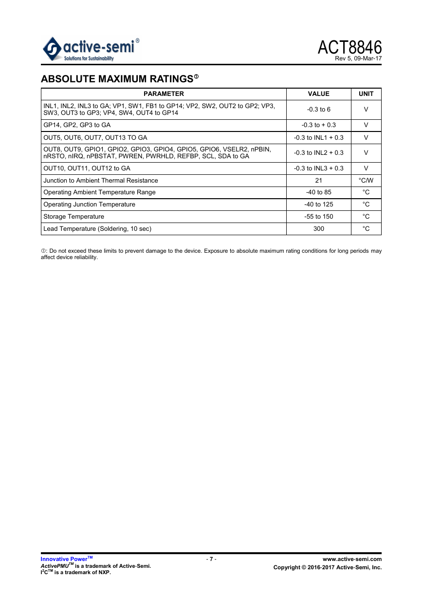
ABSOLUTE MAXIMUM RATINGS
ACT8846
Rev 5, 09-Mar-17
PARAMETER
VALUE
UNIT
INL1, INL2, INL3 to GA; VP1, SW1, FB1 to GP14; VP2, SW2, OUT2 to GP2; VP3,
SW3, OUT3 to GP3; VP4, SW4, OUT4 to GP14
GP14, GP2, GP3 to GA
OUT5, OUT6, OUT7, OUT13 TO GA
OUT8, OUT9, GPIO1, GPIO2, GPIO3, GPIO4, GPIO5, GPIO6, VSELR2, nPBIN,
nRSTO, nIRQ, nPBSTAT, PWREN, PWRHLD, REFBP, SCL, SDA to GA
OUT10, OUT11, OUT12 to GA
Junction to Ambient Thermal Resistance
Operating Ambient Temperature Range
Operating Junction Temperature
Storage Temperature
Lead Temperature (Soldering, 10 sec)
-0.3 to 6
-0.3 to + 0.3
-0.3 to INL1 + 0.3
-0.3 to INL2 + 0.3
-0.3 to INL3 + 0.3
V
V
V
V
V
21
°C/W
-40 to 85
-40 to 125
-55 to 150
300
°C
°C
°C
°C
: Do not exceed these limits to prevent damage to the device. Exposure to absolute maximum rating conditions for long periods may
affect device reliability.
Innovative PowerTM
ActivePMUTM is a trademark of Active-Semi.
I2CTM is a trademark of NXP.
- 7 -
www.active-semi.com
Copyright © 2016-2017 Active-Semi, Inc.
�
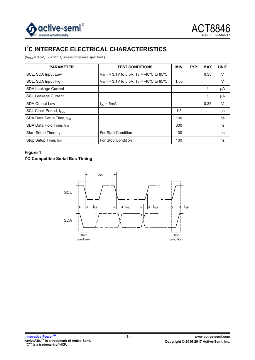
I2C INTERFACE ELECTRICAL CHARACTERISTICS
(VINL2 = 3.6V, TA = 25°C, unless otherwise specified.)
ACT8846
Rev 5, 09-Mar-17
PARAMETER
TEST CONDITIONS
MIN
TYP MAX UNIT
SCL, SDA Input Low
SCL, SDA Input High
VINL2 = 3.1V to 5.5V, TA = -40ºC to 85ºC
VINL2 = 3.1V to 5.5V, TA = -40ºC to 85ºC
1.55
SDA Leakage Current
SCL Leakage Current
SDA Output Low
IOL = 5mA
SCL Clock Period, tSCL
SDA Data Setup Time, tSU
SDA Data Hold Time, tHD
Start Setup Time, tST
Stop Setup Time, tSP
For Start Condition
For Stop Condition
Figure 1:
I2C Compatible Serial Bus Timing
1.5
100
300
100
100
0.35
1
1
0.35
V
V
µA
µA
V
µs
ns
ns
ns
ns
Innovative PowerTM
ActivePMUTM is a trademark of Active-Semi.
I2CTM is a trademark of NXP.
- 8 -
www.active-semi.com
Copyright © 2016-2017 Active-Semi, Inc.
SDASCLtSTtSUtHDtSPtSCLStart conditionStop condition�




 2023年江西萍乡中考道德与法治真题及答案.doc
 2012年重庆南川中考生物真题及答案.doc
 2013年江西师范大学地理学综合及文艺理论基础考研真题.doc
 2020年四川甘孜小升初语文真题及答案I卷.doc
 2020年注册岩土工程师专业基础考试真题及答案.doc
 2023-2024学年福建省厦门市九年级上学期数学月考试题及答案.doc
 2021-2022学年辽宁省沈阳市大东区九年级上学期语文期末试题及答案.doc
 2022-2023学年北京东城区初三第一学期物理期末试卷及答案.doc
 2018上半年江西教师资格初中地理学科知识与教学能力真题及答案.doc
 2012年河北国家公务员申论考试真题及答案-省级.doc
 2020-2021学年江苏省扬州市江都区邵樊片九年级上学期数学第一次质量检测试题及答案.doc
 2022下半年黑龙江教师资格证中学综合素质真题及答案.doc