MR25H40
4Mb Serial SPI MRAM
FEATURES
• No write delays
• Unlimited write endurance
• Data retention greater than 20 years
• Automatic data protection on power loss
• Fast, simple SPI interface with up to 40 MHz clock rate
• 3.0 to 3.6 Volt power supply range
• 3 μA sleep mode standby current
• Industrial, automotive temperatures
• Small footprint 8-pin DFN RoHS-compliant package
• Easily mounted 8-pin DIP RoHS-compliant package
• Direct replacement for serial EEPROM, Flash, FeRAM
INTRODUCTION
The MR25H40 is a 4,194,304-bit magnetoresistive random access
memory (MRAM) device organized as 524,288 words of 8 bits. The
MR25H40 offers serial EEPROM and serial Flash compatible read/write
timing with no write delays and unlimited read/write endurance.
RoHS
Unlike other serial memories, both reads and writes can occur randomly in memory with no delay between
writes. The MR25H40 is the ideal memory solution for applications that must store and retrieve data and
programs quickly using a small number of I/O pins
The MR25H40 is available in a small footprint 5 mm x 6 mm 8-pin DFN package and a 300 mil 8-pin DIP
package that is compatible with serial EEPROM, Flash, and FeRAM products.
The MR25H40 provides highly reliable data storage over a wide range of temperatures. The product is
offered with industrial temperature (-40° to +85 °C), and automotive temperature (-40° to +125° C) range
options.
CONTENTS
1. DEVICE PIN ASSIGNMENT......................................................................... 2
2. SPI COMMUNICATIONS PROTOCOL...................................................... 4
3. ELECTRICAL SPECIFICATIONS................................................................. 10
4. TIMING SPECIFICATIONS.......................................................................... 12
5. ORDERING INFORMATION....................................................................... 16
6. MECHANICAL DRAWING.......................................................................... 17
7. REVISION HISTORY...................................................................................... 19
How to Reach Us.......................................................................................... 19
Everspin Technologies © 2010
1
Document Number: MR25H40 Rev. 1, 1/2010
�
MR25H40
1. DEVICE PIN ASSIGNMENT
Overview
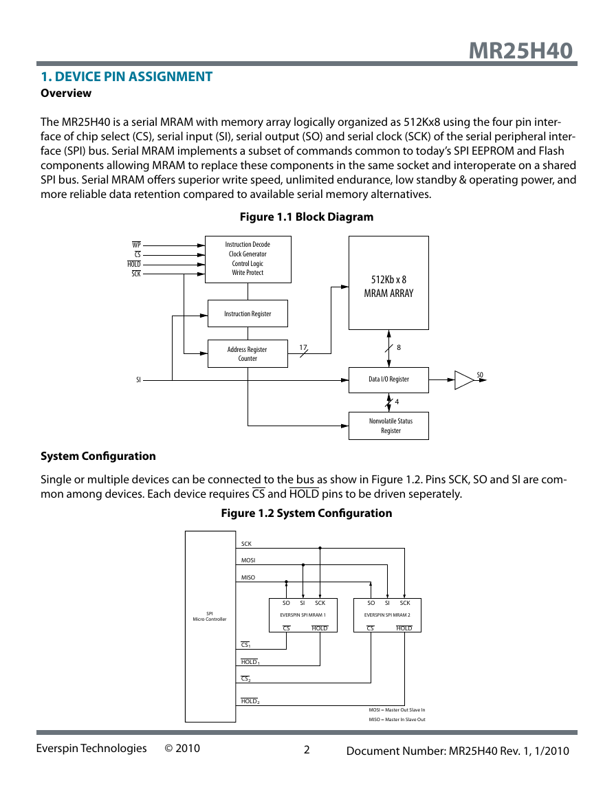
The MR25H40 is a serial MRAM with memory array logically organized as 512Kx8 using the four pin inter-
face of chip select (CS), serial input (SI), serial output (SO) and serial clock (SCK) of the serial peripheral inter-
face (SPI) bus. Serial MRAM implements a subset of commands common to today’s SPI EEPROM and Flash
components allowing MRAM to replace these components in the same socket and interoperate on a shared
SPI bus. Serial MRAM offers superior write speed, unlimited endurance, low standby & operating power, and
more reliable data retention compared to available serial memory alternatives.
Figure 1.1 Block Diagram
WP
CS
HOLD
SCK
SI
Instruction Decode
Clock Generator
Control Logic
Write Protect
Instruction Register
Address Register
Counter
17
512Kb x 8
MRAM ARRAY
8
Data I/O Register
4
Nonvolatile Status
Register
SO
System Configuration
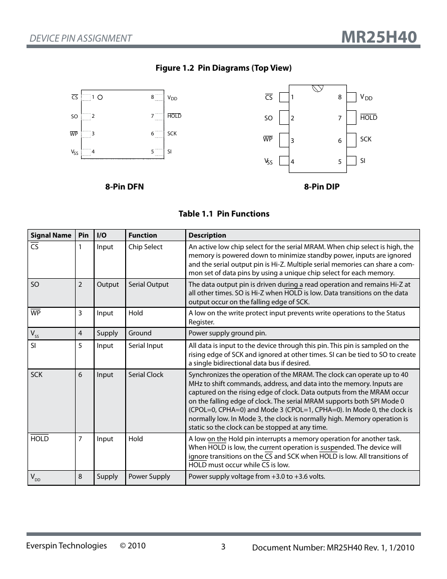
Single or multiple devices can be connected to the bus as show in Figure 1.2. Pins SCK, SO and SI are com-
mon among devices. Each device requires CS and HOLD pins to be driven seperately.
Figure 1.2 System Configuration
SPI
Micro Controller
SCK
MOSI
MISO
CS
1
HOLD
1
CS
2
HOLD
2
SO
SI
SCK
SO
SI
SCK
EVERSPIN SPI MRAM 1
EVERSPIN SPI MRAM 2
CS
HOLD
CS
HOLD
MOSI = Master Out Slave In
MISO = Master In Slave Out
Everspin Technologies © 2010
2
Document Number: MR25H40 Rev. 1, 1/2010
�
DEVICE PIN ASSIGNMENT
MR25H40
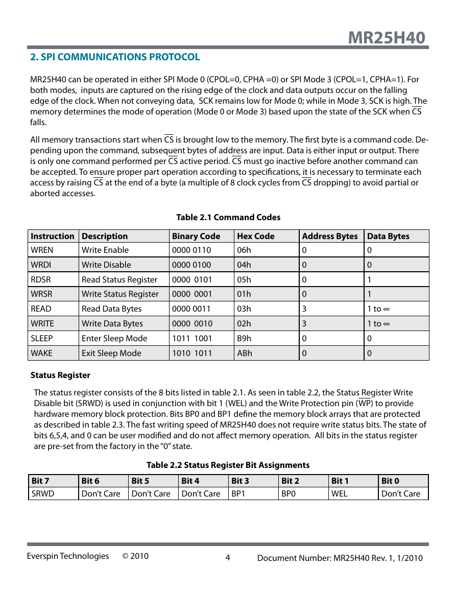
Figure 1.2 Pin Diagrams (Top View)
CS
SO
WP
V
SS
1
2
3
4
8
7
6
5
V
DD
HOLD
SCK
SI
CS
SO
WP
V
SS
1
2
3
4
8
7
6
5
V
DD
HOLD
SCK
SI
8-Pin DFN
8-Pin DIP
Table 1.1 Pin Functions
Signal Name Pin I/O
CS
1
Input
Function
Chip Select
SO
WP
VSS
SI
SCK
HOLD
VDD
2
3
4
5
6
7
8
Output
Serial Output
Input
Hold
Supply
Input
Ground
Serial Input
Input
Serial Clock
Input
Hold
Supply
Power Supply
Description
An active low chip select for the serial MRAM. When chip select is high, the
memory is powered down to minimize standby power, inputs are ignored
and the serial output pin is Hi-Z. Multiple serial memories can share a com-
mon set of data pins by using a unique chip select for each memory.
The data output pin is driven during a read operation and remains Hi-Z at
all other times. SO is Hi-Z when HOLD is low. Data transitions on the data
output occur on the falling edge of SCK.
A low on the write protect input prevents write operations to the Status
Register.
Power supply ground pin.
All data is input to the device through this pin. This pin is sampled on the
rising edge of SCK and ignored at other times. SI can be tied to SO to create
a single bidirectional data bus if desired.
Synchronizes the operation of the MRAM. The clock can operate up to 40
MHz to shift commands, address, and data into the memory. Inputs are
captured on the rising edge of clock. Data outputs from the MRAM occur
on the falling edge of clock. The serial MRAM supports both SPI Mode 0
(CPOL=0, CPHA=0) and Mode 3 (CPOL=1, CPHA=0). In Mode 0, the clock is
normally low. In Mode 3, the clock is normally high. Memory operation is
static so the clock can be stopped at any time.
A low on the Hold pin interrupts a memory operation for another task.
When HOLD is low, the current operation is suspended. The device will
ignore transitions on the CS and SCK when HOLD is low. All transitions of
HOLD must occur while CS is low.
Power supply voltage from +3.0 to +3.6 volts.
Everspin Technologies © 2010
3
Document Number: MR25H40 Rev. 1, 1/2010
�
MR25H40
2. SPI COMMUNICATIONS PROTOCOL
MR25H40 can be operated in either SPI Mode 0 (CPOL=0, CPHA =0) or SPI Mode 3 (CPOL=1, CPHA=1). For
both modes, inputs are captured on the rising edge of the clock and data outputs occur on the falling
edge of the clock. When not conveying data, SCK remains low for Mode 0; while in Mode 3, SCK is high. The
memory determines the mode of operation (Mode 0 or Mode 3) based upon the state of the SCK when CS
falls.
All memory transactions start when CS is brought low to the memory. The first byte is a command code. De-
pending upon the command, subsequent bytes of address are input. Data is either input or output. There
is only one command performed per CS active period. CS must go inactive before another command can
be accepted. To ensure proper part operation according to specifications, it is necessary to terminate each
access by raising CS at the end of a byte (a multiple of 8 clock cycles from CS dropping) to avoid partial or
aborted accesses.
Table 2.1 Command Codes
Instruction Description
WREN
Write Enable
Write Disable
WRDI
RDSR
Read Status Register
Write Status Register
WRSR
Read Data Bytes
READ
WRITE
Write Data Bytes
Enter Sleep Mode
SLEEP
WAKE
Exit Sleep Mode
Binary Code
0000 0110
0000 0100
0000 0101
0000 0001
0000 0011
0000 0010
1011 1001
1010 1011
Hex Code
06h
04h
05h
01h
03h
02h
B9h
ABh
Address Bytes Data Bytes
0
0
0
0
3
3
0
0
0
0
1
1
1 to ∞
1 to ∞
0
0
Status Register
The status register consists of the 8 bits listed in table 2.1. As seen in table 2.2, the Status Register Write
Disable bit (SRWD) is used in conjunction with bit 1 (WEL) and the Write Protection pin (WP) to provide
hardware memory block protection. Bits BP0 and BP1 define the memory block arrays that are protected
as described in table 2.3. The fast writing speed of MR25H40 does not require write status bits. The state of
bits 6,5,4, and 0 can be user modified and do not affect memory operation. All bits in the status register
are pre-set from the factory in the “0” state.
Table 2.2 Status Register Bit Assignments
Bit 7
SRWD
Bit 6
Don’t Care Don’t Care Don’t Care
Bit 5
Bit 4
Bit 3
BP1
Bit 2
BP0
Bit 1
WEL
Bit 0
Don’t Care
Everspin Technologies © 2010
4
Document Number: MR25H40 Rev. 1, 1/2010
�
SPI COMMUNICATIONS PROTOCOL
Table 2.3 Memory Protection Modes
WEL
SRWD WP
Protected Blocks
Unprotected Blocks
X
0
1
1
X
X
Low
High
Protected
Protected
Protected
Protected
Table 2.4 Block Memory Write Protection
Protected
Writable
Writable
Writable
Status Register
Memory Contents
MR25H40
Status
Register
Protected
Writable
Protected
Writable
0
1
1
1
BP1
0
0
1
1
BP0
0
1
0
1
Protected Area
None
Upper Quarter
Upper Half
All
Unprotected Area
All Memory
Lower Three-Quarters
Lower Half
None
Block Protection
The memory enters hardware block protection when the WP input is low and the Status Register Write Dis-
able (SRWD) bit is set to 0. The memory leaves hardware block protection only when the WP pin goes high.
While WP is low, the write protection blocks for the memory are determined by the status register bits BP0
and BP1 and cannot be modified without taking the WP signal high again.
If the WP signal is high (independent of the status of SRWD bit), the memory is in software protection
mode. This means that block write protection is controlled solely by the status register BP0 and BP1 block
write protect bits and this information can be modified using the WRSR command.
Read Status Register (RDSR)
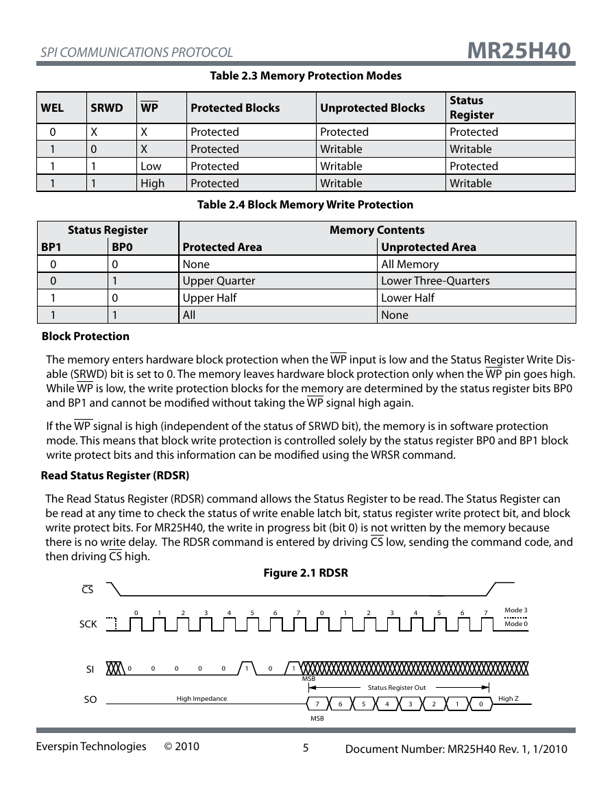
The Read Status Register (RDSR) command allows the Status Register to be read. The Status Register can
be read at any time to check the status of write enable latch bit, status register write protect bit, and block
write protect bits. For MR25H40, the write in progress bit (bit 0) is not written by the memory because
there is no write delay. The RDSR command is entered by driving CS low, sending the command code, and
then driving CS high.
Figure 2.1 RDSR
CS
SCK
SI
SO
0
1
2
3
4
5
6
7
0
1
2
3
4
5
6
7
Mode 3
Mode 0
0
0
0
0
0
1
0
1
MSB
Status Register Out
High Impedance
7
6
5
4
3
2
1
0
High Z
Everspin Technologies © 2010
MSB
5
Document Number: MR25H40 Rev. 1, 1/2010
�
SPI COMMUNICATIONS PROTOCOL
Write Enable (WREN)
MR25H40
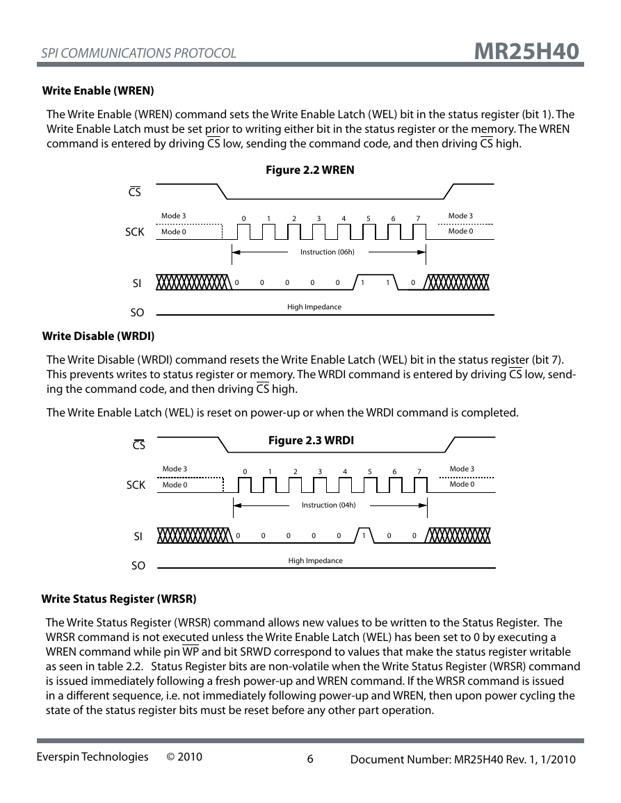
The Write Enable (WREN) command sets the Write Enable Latch (WEL) bit in the status register (bit 1). The
Write Enable Latch must be set prior to writing either bit in the status register or the memory. The WREN
command is entered by driving CS low, sending the command code, and then driving CS high.
Figure 2.2 WREN
CS
SCK
SI
SO
Mode 3
Mode 0
0
1
2
3
4
5
6
7
Mode 3
Mode 0
Instruction (06h)
0
0
0
0
0
1
1
0
High Impedance
Write Disable (WRDI)
The Write Disable (WRDI) command resets the Write Enable Latch (WEL) bit in the status register (bit 7).
This prevents writes to status register or memory. The WRDI command is entered by driving CS low, send-
ing the command code, and then driving CS high.
The Write Enable Latch (WEL) is reset on power-up or when the WRDI command is completed.
Figure 2.3 WRDI
Mode 3
Mode 0
0
1
2
3
4
5
6
7
Mode 3
Mode 0
Instruction (04h)
0
0
0
0
0
1
0
0
High Impedance
CS
SCK
SI
SO
Write Status Register (WRSR)
The Write Status Register (WRSR) command allows new values to be written to the Status Register. The
WRSR command is not executed unless the Write Enable Latch (WEL) has been set to 0 by executing a
WREN command while pin WP and bit SRWD correspond to values that make the status register writable
as seen in table 2.2. Status Register bits are non-volatile when the Write Status Register (WRSR) command
is issued immediately following a fresh power-up and WREN command. If the WRSR command is issued
in a different sequence, i.e. not immediately following power-up and WREN, then upon power cycling the
state of the status register bits must be reset before any other part operation.
Everspin Technologies © 2010
6
Document Number: MR25H40 Rev. 1, 1/2010
�
SPI COMMUNICATIONS PROTOCOL
MR25H40
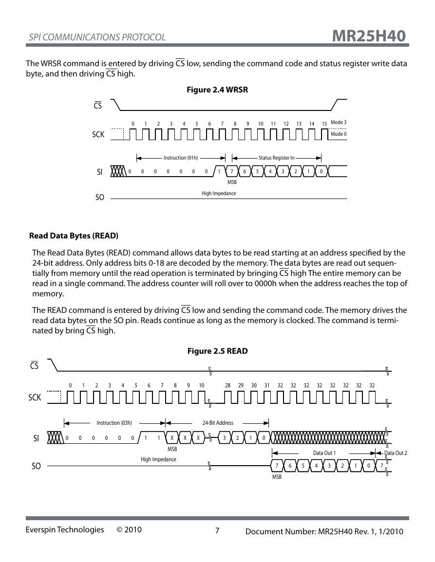
The WRSR command is entered by driving CS low, sending the command code and status register write data
byte, and then driving CS high.
Figure 2.4 WRSR
CS
SCK
SI
SO
0
1
2
3
4
5
6
7
8
9
10
11
12
13
14
15
Mode 3
Mode 0
Instruction (01h)
Status Register In
0
0
0
0
0
0
0
1
7
6
5
4
3
2
1
0
MSB
High Impedance
Read Data Bytes (READ)
The Read Data Bytes (READ) command allows data bytes to be read starting at an address specified by the
24-bit address. Only address bits 0-18 are decoded by the memory. The data bytes are read out sequen-
tially from memory until the read operation is terminated by bringing CS high The entire memory can be
read in a single command. The address counter will roll over to 0000h when the address reaches the top of
memory.
The READ command is entered by driving CS low and sending the command code. The memory drives the
read data bytes on the SO pin. Reads continue as long as the memory is clocked. The command is termi-
nated by bring CS high.
Figure 2.5 READ
CS
SCK
SI
SO
0
1
2
3
4
5
6
7
8
9
10
28
29
30
31
32
32
32
32
32
32
32
32
Instruction (03h)
24-Bit Address
0
0
0
0
0
0
1
1
X
X
X
3
2
1
0
MSB
High Impedance
Data Out 1
Data Out 2
6
5
4
3
2
1
0
7
7
MSB
Everspin Technologies © 2010
7
Document Number: MR25H40 Rev. 1, 1/2010
�
SPI COMMUNICATIONS PROTOCOL
MR25H40
Write Data Bytes (WRITE)
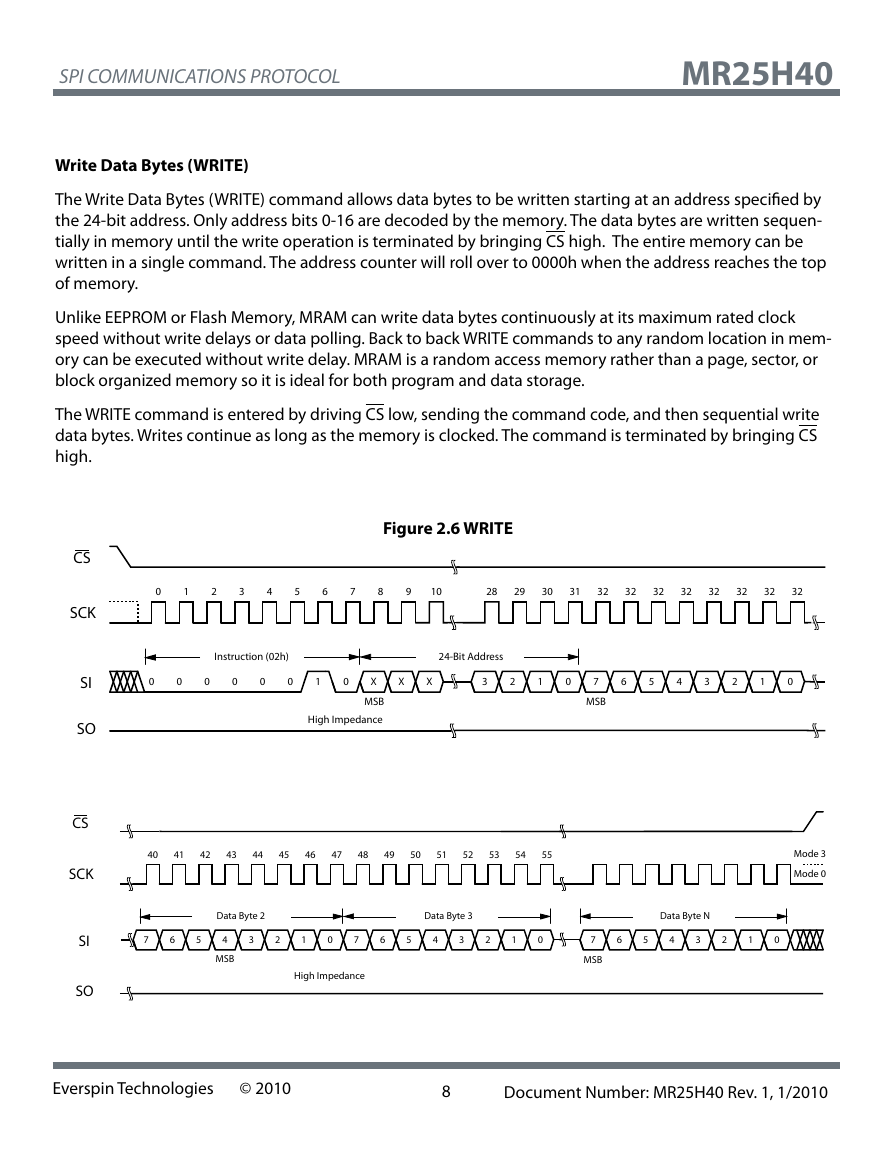
The Write Data Bytes (WRITE) command allows data bytes to be written starting at an address specified by
the 24-bit address. Only address bits 0-16 are decoded by the memory. The data bytes are written sequen-
tially in memory until the write operation is terminated by bringing CS high. The entire memory can be
written in a single command. The address counter will roll over to 0000h when the address reaches the top
of memory.
Unlike EEPROM or Flash Memory, MRAM can write data bytes continuously at its maximum rated clock
speed without write delays or data polling. Back to back WRITE commands to any random location in mem-
ory can be executed without write delay. MRAM is a random access memory rather than a page, sector, or
block organized memory so it is ideal for both program and data storage.
The WRITE command is entered by driving CS low, sending the command code, and then sequential write
data bytes. Writes continue as long as the memory is clocked. The command is terminated by bringing CS
high.
Figure 2.6 WRITE
0
1
2
3
4
5
6
7
8
9
10
28
29
30
31
32
32
32
32
32
32
32
32
Instruction (02h)
24-Bit Address
0
0
0
0
0
0
1
0
X
X
X
3
2
1
0
7
6
5
4
3
2
1
0
MSB
High Impedance
MSB
40
41
42
43
44
45
46
47
48
49
50
51
52
53
54
55
Mode 3
Mode 0
Data Byte 2
Data Byte 3
Data Byte N
7
6
5
4
3
2
1
0
7
6
5
4
3
2
1
0
7
6
5
4
3
2
1
0
MSB
High Impedance
MSB
CS
SCK
SI
SO
CS
SCK
SI
SO
Everspin Technologies © 2010
8
Document Number: MR25H40 Rev. 1, 1/2010
�



 2023年江西萍乡中考道德与法治真题及答案.doc
 2012年重庆南川中考生物真题及答案.doc
 2013年江西师范大学地理学综合及文艺理论基础考研真题.doc
 2020年四川甘孜小升初语文真题及答案I卷.doc
 2020年注册岩土工程师专业基础考试真题及答案.doc
 2023-2024学年福建省厦门市九年级上学期数学月考试题及答案.doc
 2021-2022学年辽宁省沈阳市大东区九年级上学期语文期末试题及答案.doc
 2022-2023学年北京东城区初三第一学期物理期末试卷及答案.doc
 2018上半年江西教师资格初中地理学科知识与教学能力真题及答案.doc
 2012年河北国家公务员申论考试真题及答案-省级.doc
 2020-2021学年江苏省扬州市江都区邵樊片九年级上学期数学第一次质量检测试题及答案.doc
 2022下半年黑龙江教师资格证中学综合素质真题及答案.doc