®
RT9065
500mA, Low Dropout, Low Noise, Ultra-Fast Linear Regulator
General Description
The RT9065 is designed for portable RF and wireless
applications with demanding performance and space
requirements. The RT9065 performance is optimized for
battery powered systems to deliver ultra low noise and
low quiescent current. A noise bypass pin is available for
further reduction of output noise. Regulator ground current
increases only slightly in dropout, further prolonging the
battery life. The RT9065 also works with low-ESR ceramic
capacitors, reducing the amount of board space necessary
for power applications, critical in hand held wireless
devices. The RT9065 consumes less than 0.01μA in
shutdown mode and has fast turn-on time less than 10μs.
The other features include low dropout voltage, high output
accuracy, current limiting protection, and high ripple
rejection ratio. The RT9065 is available in the SOT-23-6
package.
Features
Ultra-Low-Noise for RF Application
Ultra-Fast Response in Line/Load Transient
Quick Start-Up (Typically 10μμμμμs)
0.01μμμμμA Shutdown Current
Low Dropout : 370mV @ 500mA
Wide Input Voltage Range : 2.2V to 5.5V
Adjustable Output Voltage
TTL Logic Controlled Shutdown Input
Low Temperature Coefficient
Current Limiting Protection
Thermal Shutdown Protection
Only 1μμμμμF Output Capacitor Required for Stability
High Power Supply Rejection Ratio
RoHS Compliant and Halogen Free
Ordering Information
RT9065
Package Type
E : SOT-23-6
Lead Plating System
G : Green (Halogen Free and Pb Free)
Note :
Richtek products are :
RoHS compliant and compatible with the current require-
ments of IPC/JEDEC J-STD-020.
Suitable for use in SnPb or Pb-free soldering processes.
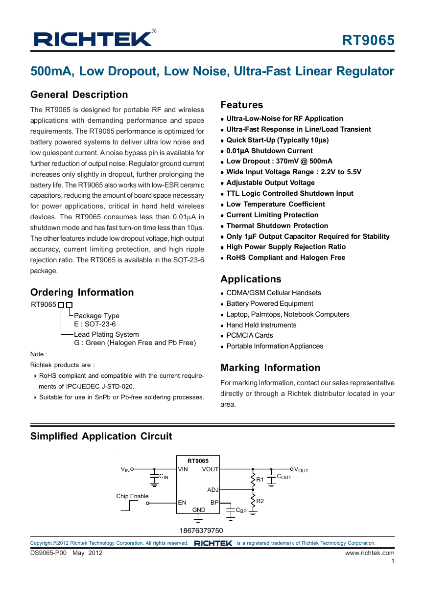
Simplified Application Circuit
Applications
CDMA/GSM Cellular Handsets
Battery Powered Equipment
Laptop, Palmtops, Notebook Computers
Hand Held Instruments
PCMCIA Cards
Portable Information Appliances
Marking Information
For marking information, contact our sales representative
directly or through a Richtek distributor located in your
area.
VIN
CIN
Chip Enable
RT9065
VIN
VOUT
ADJ
BP
EN
GND
18676379750
VOUT
COUT
R1
R2
CBP
©
Copyright 2012 Richtek Technology Corporation. All rights reserved. is a registered trademark of Richtek Technology Corporation.
DS9065-P00 May 2012
www.richtek.com
1
�
RT9065
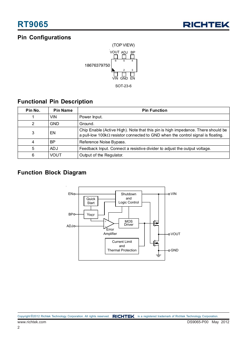
Pin Configurations
(TOP VIEW)
VOUT ADJ BP
18676379750
6
5
2
4
3
VIN GND EN
SOT-23-6
Functional Pin Description
Pin No.
Pin Name
Pin Function
1
2
3
4
5
6
VIN
GND
EN
BP
ADJ
VOUT
Power Input.
Ground.
Chip Enable (Active High). Note that this pin is high impedance. There should be
a pull-low 100kΩ resistor connected to GND when the control signal is floating.
Reference Noise Bypass.
Feedback Input. Connect a resistive divider to adjust the output voltage.
Output of the Regulator.
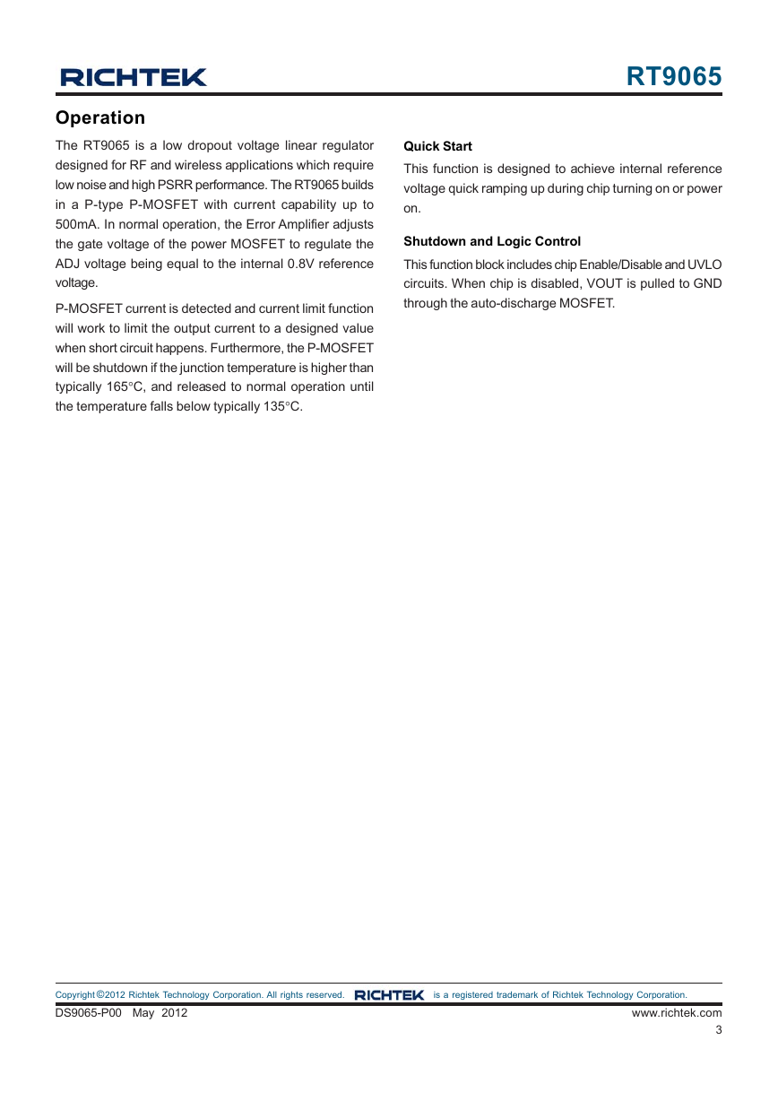
Function Block Diagram
EN
BP
ADJ
Quick
Start
VREF
Shutdown
and
Logic Control
MOS
Driver
+
-
Error
Amplifier
Current Limit
and
Thermal Protection
VIN
VOUT
GND
©
Copyright 2012 Richtek Technology Corporation. All rights reserved. is a registered trademark of Richtek Technology Corporation.
www.richtek.com
2
DS9065-P00 May 2012
�
RT9065
Quick Start
This function is designed to achieve internal reference
voltage quick ramping up during chip turning on or power
on.
Shutdown and Logic Control
This function block includes chip Enable/Disable and UVLO
circuits. When chip is disabled, VOUT is pulled to GND
through the auto-discharge MOSFET.
Operation
The RT9065 is a low dropout voltage linear regulator
designed for RF and wireless applications which require
low noise and high PSRR performance. The RT9065 builds
in a P-type P-MOSFET with current capability up to
500mA. In normal operation, the Error Amplifier adjusts
the gate voltage of the power MOSFET to regulate the
ADJ voltage being equal to the internal 0.8V reference
voltage.
P-MOSFET current is detected and current limit function
will work to limit the output current to a designed value
when short circuit happens. Furthermore, the P-MOSFET
will be shutdown if the junction temperature is higher than
typically 165°C, and released to normal operation until
the temperature falls below typically 135°C.
©
Copyright 2012 Richtek Technology Corporation. All rights reserved. is a registered trademark of Richtek Technology Corporation.
DS9065-P00 May 2012
www.richtek.com
3
�
RT9065
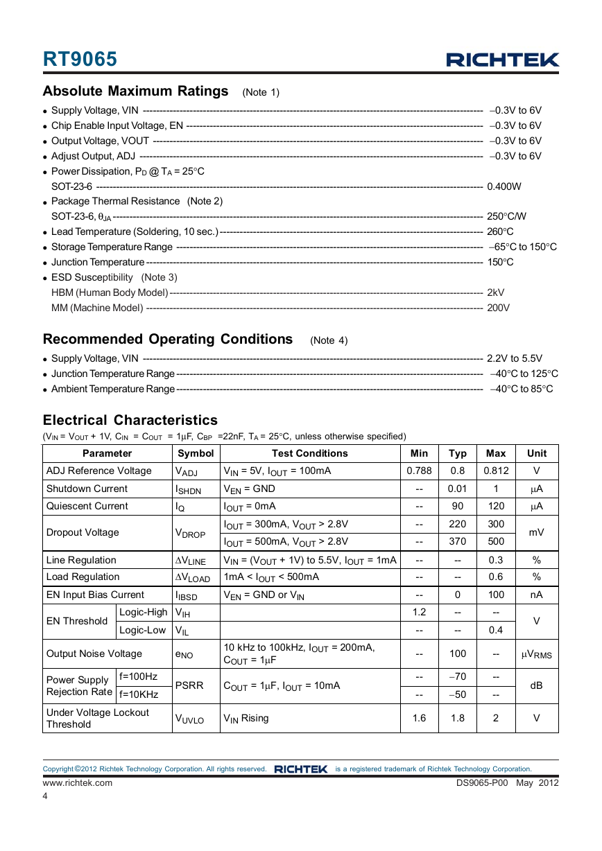
Absolute Maximum Ratings (Note 1)
Supply Voltage, VIN ------------------------------------------------------------------------------------------------------ −0.3V to 6V
Chip Enable Input Voltage, EN ----------------------------------------------------------------------------------------- −0.3V to 6V
Output Voltage, VOUT --------------------------------------------------------------------------------------------------- −0.3V to 6V
Adjust Output, ADJ ------------------------------------------------------------------------------------------------------- −0.3V to 6V
Power Dissipation, PD @ TA = 25°C
SOT-23-6 -------------------------------------------------------------------------------------------------------------------- 0.400W
Package Thermal Resistance (Note 2)
SOT-23-6, θJA --------------------------------------------------------------------------------------------------------------- 250°C/W
Lead Temperature (Soldering, 10 sec.) ------------------------------------------------------------------------------- 260°C
Storage Temperature Range -------------------------------------------------------------------------------------------- −65°C to 150°C
Junction Temperature ----------------------------------------------------------------------------------------------------- 150°C
ESD Susceptibility (Note 3)
HBM (Human Body Model) ---------------------------------------------------------------------------------------------- 2kV
MM (Machine Model) ----------------------------------------------------------------------------------------------------- 200V
Recommended Operating Conditions (Note 4)
Supply Voltage, VIN ------------------------------------------------------------------------------------------------------ 2.2V to 5.5V
Junction Temperature Range--------------------------------------------------------------------------------------------
Ambient Temperature Range--------------------------------------------------------------------------------------------
−40°C to 125°C
−40°C to 85°C
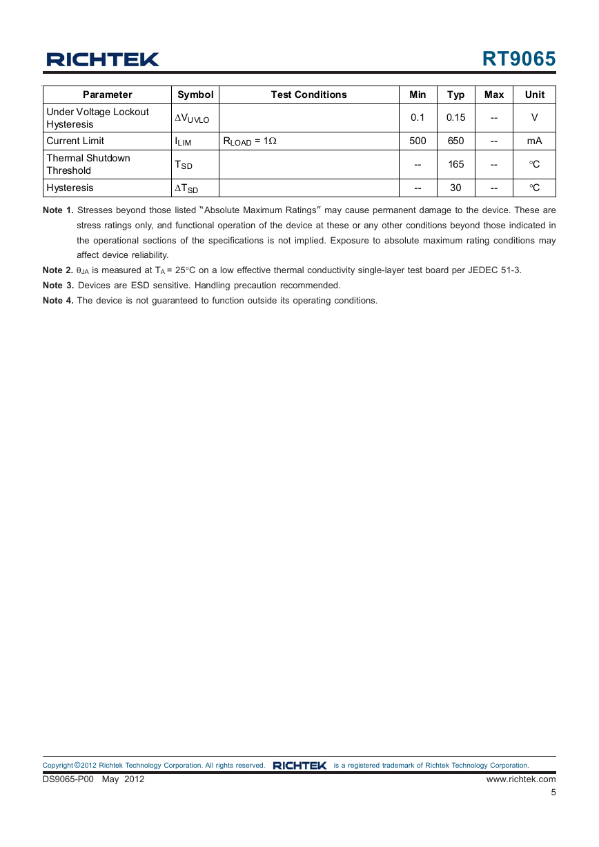
Electrical Characteristics
(VIN = VOUT + 1V, CIN = COUT = 1μF, CBP =22nF, TA = 25°C, unless otherwise specified)
Parameter
ADJ Reference Voltage
Shutdown Current
Quiescent Current
Dropout Voltage
Symbol
VADJ
ISHDN
IQ
VDROP
Test Conditions
VIN = 5V, IOUT = 100mA
VEN = GND
IOUT = 0mA
IOUT = 300mA, VOUT > 2.8V
IOUT = 500mA, VOUT > 2.8V
VIN = (VOUT + 1V) to 5.5V, IOUT = 1mA
Line Regulation
Load Regulation
EN Input Bias Current
EN Threshold
ΔVLINE
ΔVLOAD 1mA < IOUT < 500mA
IIBSD
Logic-High VIH
Logic-Low VIL
VEN = GND or VIN
10 kHz to 100kHz, IOUT = 200mA,
COUT = 1μF
Output Noise Voltage
eNO
f=100Hz
Power Supply
Rejection Rate f=10KHz
Under Voltage Lockout
Threshold
PSRR
COUT = 1μF, IOUT = 10mA
VUVLO
VIN Rising
Min
0.788
--
--
--
--
--
--
--
1.2
--
--
--
--
1.6
Typ Max
0.8
0.812
0.01
90
220
370
--
--
0
--
--
1
120
300
500
0.3
0.6
100
--
0.4
Unit
V
μA
μA
mV
%
%
nA
V
100
−70
−50
1.8
--
--
--
2
μVRMS
dB
V
©
Copyright 2012 Richtek Technology Corporation. All rights reserved. is a registered trademark of Richtek Technology Corporation.
www.richtek.com
4
DS9065-P00 May 2012
�
Parameter
Symbol
Test Conditions
Under Voltage Lockout
Hysteresis
Current Limit
Thermal Shutdown
Threshold
Hysteresis
ΔVUVLO
ILIM
TSD
ΔTSD
RLOAD = 1Ω
RT9065
Min
0.1
500
--
--
Typ Max
Unit
0.15
650
165
30
--
--
--
--
V
mA
°C
°C
Note 1. Stresses beyond those listed “Absolute Maximum Ratings” may cause permanent damage to the device. These are
stress ratings only, and functional operation of the device at these or any other conditions beyond those indicated in
the operational sections of the specifications is not implied. Exposure to absolute maximum rating conditions may
affect device reliability.
Note 2. θJA is measured at TA = 25°C on a low effective thermal conductivity single-layer test board per JEDEC 51-3.
Note 3. Devices are ESD sensitive. Handling precaution recommended.
Note 4. The device is not guaranteed to function outside its operating conditions.
©
Copyright 2012 Richtek Technology Corporation. All rights reserved. is a registered trademark of Richtek Technology Corporation.
DS9065-P00 May 2012
www.richtek.com
5
�
RT9065
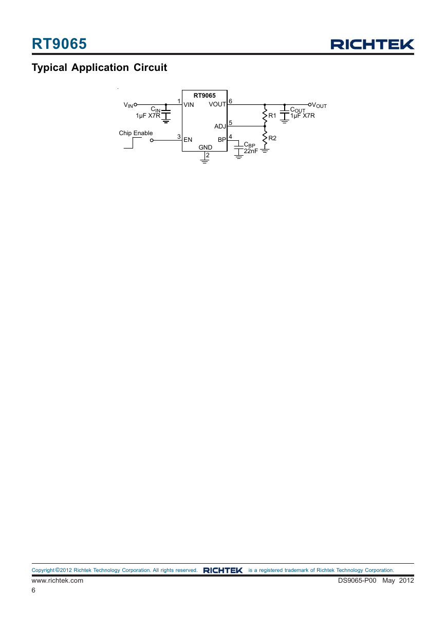
Typical Application Circuit
VIN
CIN
1µF X7R
Chip Enable
RT9065
VIN
VOUT
1
ADJ
BP
3
EN
GND
2
6
5
4
R1
R2
CBP
22nF
VOUT
COUT
1µF X7R
©
Copyright 2012 Richtek Technology Corporation. All rights reserved. is a registered trademark of Richtek Technology Corporation.
www.richtek.com
6
DS9065-P00 May 2012
�
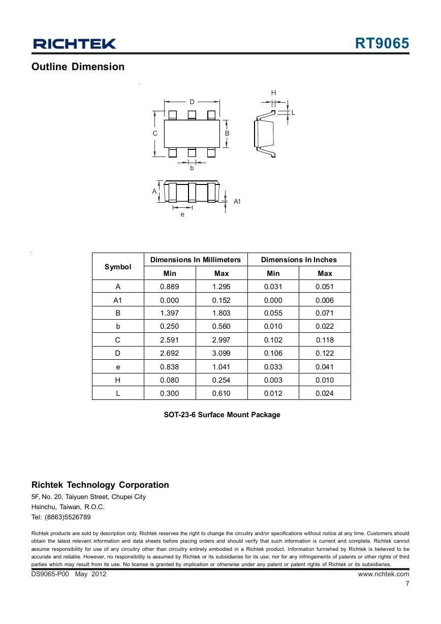
Outline Dimension
RT9065
H
L
C
A
D
b
e
B
A1
Symbol
A
A1
B
b
C
D
e
H
L
Dimensions In Millimeters
Dimensions In Inches
Min
0.889
0.000
1.397
0.250
2.591
2.692
0.838
0.080
0.300
Max
1.295
0.152
1.803
0.560
2.997
3.099
1.041
0.254
0.610
Min
0.031
0.000
0.055
0.010
0.102
0.106
0.033
0.003
0.012
Max
0.051
0.006
0.071
0.022
0.118
0.122
0.041
0.010
0.024
SOT-23-6 Surface Mount Package
Richtek Technology Corporation
5F, No. 20, Taiyuen Street, Chupei City
Hsinchu, Taiwan, R.O.C.
Tel: (8863)5526789
Richtek products are sold by description only. Richtek reserves the right to change the circuitry and/or specifications without notice at any time. Customers should
obtain the latest relevant information and data sheets before placing orders and should verify that such information is current and complete. Richtek cannot
assume responsibility for use of any circuitry other than circuitry entirely embodied in a Richtek product. Information furnished by Richtek is believed to be
accurate and reliable. However, no responsibility is assumed by Richtek or its subsidiaries for its use; nor for any infringements of patents or other rights of third
parties which may result from its use. No license is granted by implication or otherwise under any patent or patent rights of Richtek or its subsidiaries.
DS9065-P00 May 2012
www.richtek.com
7
�
RT9065
Datasheet Revision History
Version
P00
Data
Page No.
2012/5/25
Item
Description
first edition
©
Copyright 2012 Richtek Technology Corporation. All rights reserved. is a registered trademark of Richtek Technology Corporation.
www.richtek.com
8
DS9065-P00 May 2012
�


 2023年江西萍乡中考道德与法治真题及答案.doc
 2012年重庆南川中考生物真题及答案.doc
 2013年江西师范大学地理学综合及文艺理论基础考研真题.doc
 2020年四川甘孜小升初语文真题及答案I卷.doc
 2020年注册岩土工程师专业基础考试真题及答案.doc
 2023-2024学年福建省厦门市九年级上学期数学月考试题及答案.doc
 2021-2022学年辽宁省沈阳市大东区九年级上学期语文期末试题及答案.doc
 2022-2023学年北京东城区初三第一学期物理期末试卷及答案.doc
 2018上半年江西教师资格初中地理学科知识与教学能力真题及答案.doc
 2012年河北国家公务员申论考试真题及答案-省级.doc
 2020-2021学年江苏省扬州市江都区邵樊片九年级上学期数学第一次质量检测试题及答案.doc
 2022下半年黑龙江教师资格证中学综合素质真题及答案.doc