SOLUTIONS MANUAL
OPERATING SYSTEMS:
INTERNALS AND DESIGN PRINCIPLES
FIFTH EDITION
WILLIAM STALLINGS
Copyright 2004: William Stallings
�
© 2004 by William Stallings
All rights reserved. No part of this document may be reproduced, in any
form or by any means, or posted on the Internet, without permission in
writing from the author.
-2-
�
NOTICE
This manual contains solutions to all of the review questions and
homework problems in Operating Systems, Fifth Edition. If you spot an
error in a solution or in the wording of a problem, I would greatly
appreciate it if you would forward the information via email to me at
ws@shore.net. An errata sheet for this manual, if needed, is available at
ftp://shell.shore.net/members/w/s/ws/S/
W.S.
-3-
�
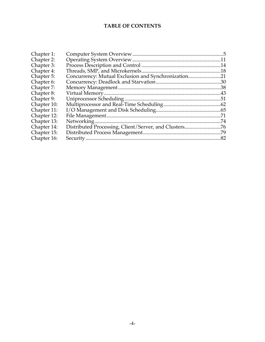
TABLE OF CONTENTS
Computer System Overview......................................................................5
Chapter 1:
Operating System Overview....................................................................11
Chapter 2:
Process Description and Control .............................................................14
Chapter 3:
Threads, SMP, and Microkernels.............................................................18
Chapter 4:
Concurrency: Mutual Exclusion and Synchronization.........................21
Chapter 5:
Concurrency: Deadlock and Starvation..................................................30
Chapter 6:
Memory Management...............................................................................38
Chapter 7:
Virtual Memory..........................................................................................43
Chapter 8:
Uniprocessor Scheduling..........................................................................51
Chapter 9:
Chapter 10: Multiprocessor and Real-Time Scheduling............................................62
Chapter 11:
I/O Management and Disk Scheduling..................................................65
Chapter 12:
File Management........................................................................................71
Chapter 13: Networking.................................................................................................74
Distributed Processing, Client/Server, and Clusters............................76
Chapter 14:
Chapter 15:
Distributed Process Management............................................................79
Chapter 16:
Security........................................................................................................82
-4-
�
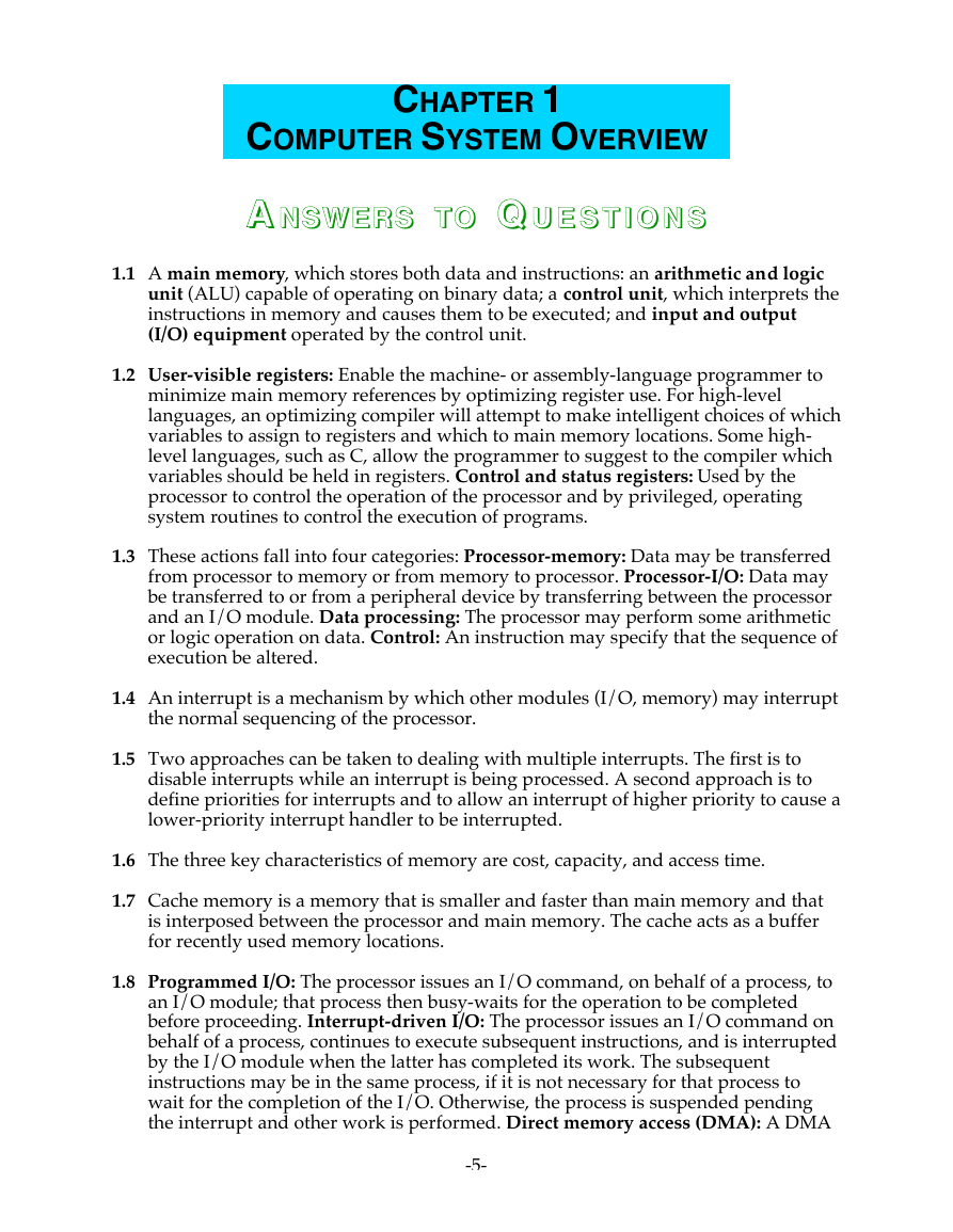
CHAPTER 1
COMPUTER SYSTEM OVERVIEW
AA NSWERS TO
NSWERS TO QQ U E S T I O N S
U E S T I O N S
1.1 A main memory, which stores both data and instructions: an arithmetic and logic
unit (ALU) capable of operating on binary data; a control unit, which interprets the
instructions in memory and causes them to be executed; and input and output
(I/O) equipment operated by the control unit.
1.2 User-visible registers: Enable the machine- or assembly-language programmer to
minimize main memory references by optimizing register use. For high-level
languages, an optimizing compiler will attempt to make intelligent choices of which
variables to assign to registers and which to main memory locations. Some high-
level languages, such as C, allow the programmer to suggest to the compiler which
variables should be held in registers. Control and status registers: Used by the
processor to control the operation of the processor and by privileged, operating
system routines to control the execution of programs.
1.3 These actions fall into four categories: Processor-memory: Data may be transferred
from processor to memory or from memory to processor. Processor-I/O: Data may
be transferred to or from a peripheral device by transferring between the processor
and an I/O module. Data processing: The processor may perform some arithmetic
or logic operation on data. Control: An instruction may specify that the sequence of
execution be altered.
1.4 An interrupt is a mechanism by which other modules (I/O, memory) may interrupt
the normal sequencing of the processor.
1.5 Two approaches can be taken to dealing with multiple interrupts. The first is to
disable interrupts while an interrupt is being processed. A second approach is to
define priorities for interrupts and to allow an interrupt of higher priority to cause a
lower-priority interrupt handler to be interrupted.
1.6 The three key characteristics of memory are cost, capacity, and access time.
1.7 Cache memory is a memory that is smaller and faster than main memory and that
is interposed between the processor and main memory. The cache acts as a buffer
for recently used memory locations.
1.8 Programmed I/O: The processor issues an I/O command, on behalf of a process, to
an I/O module; that process then busy-waits for the operation to be completed
before proceeding. Interrupt-driven I/O: The processor issues an I/O command on
behalf of a process, continues to execute subsequent instructions, and is interrupted
by the I/O module when the latter has completed its work. The subsequent
instructions may be in the same process, if it is not necessary for that process to
wait for the completion of the I/O. Otherwise, the process is suspended pending
the interrupt and other work is performed. Direct memory access (DMA): A DMA
-5-
�
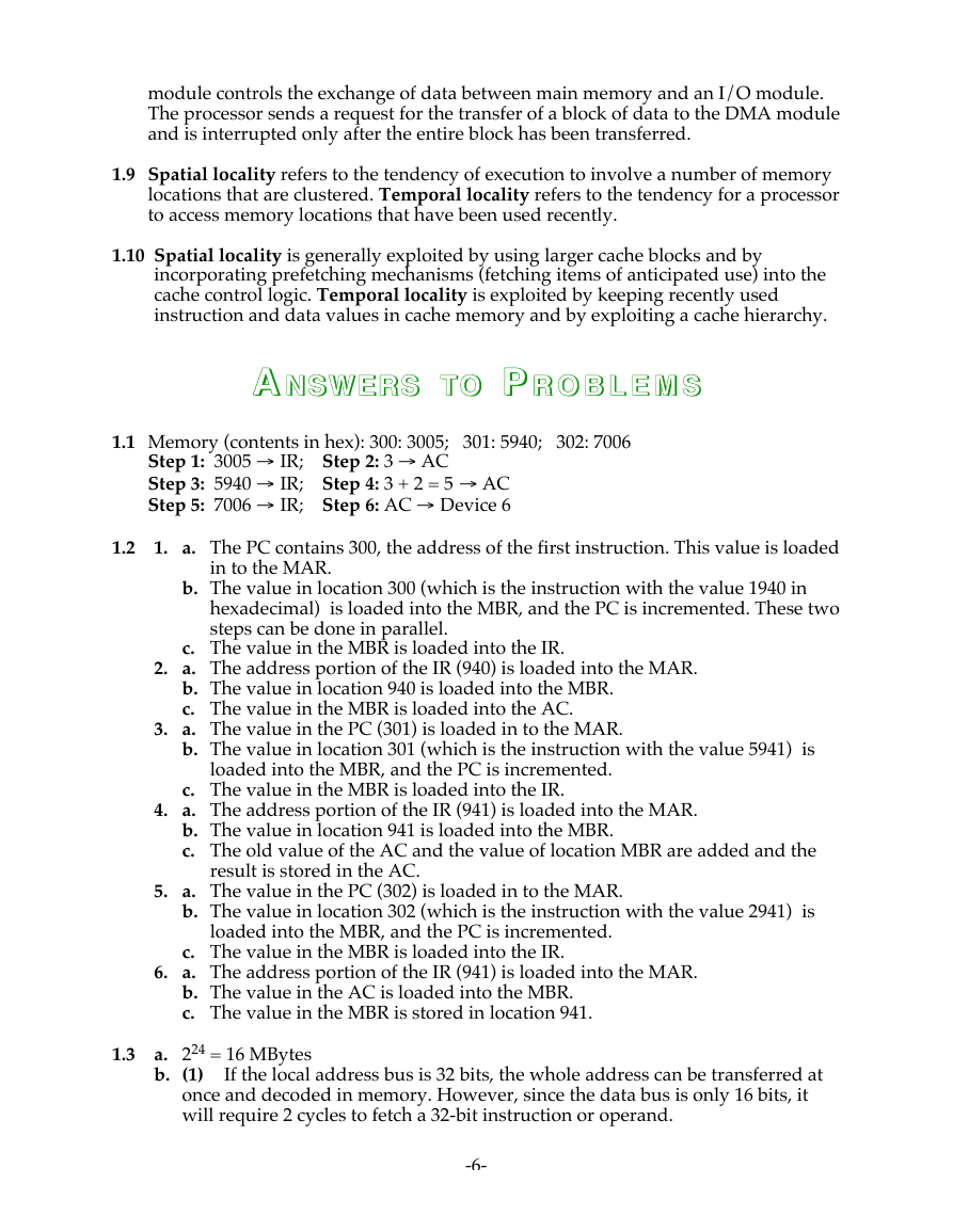
module controls the exchange of data between main memory and an I/O module.
The processor sends a request for the transfer of a block of data to the DMA module
and is interrupted only after the entire block has been transferred.
1.9 Spatial locality refers to the tendency of execution to involve a number of memory
locations that are clustered. Temporal locality refers to the tendency for a processor
to access memory locations that have been used recently.
1.10 Spatial locality is generally exploited by using larger cache blocks and by
incorporating prefetching mechanisms (fetching items of anticipated use) into the
cache control logic. Temporal locality is exploited by keeping recently used
instruction and data values in cache memory and by exploiting a cache hierarchy.
AA NSWERS TO
NSWERS TO PP R O B L E M S
R O B L E M S
1.1 Memory (contents in hex): 300: 3005; 301: 5940; 302: 7006
Step 1: 3005 → IR; Step 2: 3 → AC
Step 3: 5940 → IR; Step 4: 3 + 2 = 5 → AC
Step 5: 7006 → IR; Step 6: AC → Device 6
1. a. The PC contains 300, the address of the first instruction. This value is loaded
b. The value in location 300 (which is the instruction with the value 1940 in
in to the MAR.
hexadecimal) is loaded into the MBR, and the PC is incremented. These two
steps can be done in parallel.
2. a. The address portion of the IR (940) is loaded into the MAR.
c. The value in the MBR is loaded into the IR.
b. The value in location 940 is loaded into the MBR.
c. The value in the MBR is loaded into the AC.
3. a. The value in the PC (301) is loaded in to the MAR.
b. The value in location 301 (which is the instruction with the value 5941) is
loaded into the MBR, and the PC is incremented.
c. The value in the MBR is loaded into the IR.
b. The value in location 941 is loaded into the MBR.
c. The old value of the AC and the value of location MBR are added and the
4. a. The address portion of the IR (941) is loaded into the MAR.
1.2
1.3
result is stored in the AC.
5. a. The value in the PC (302) is loaded in to the MAR.
loaded into the MBR, and the PC is incremented.
b. The value in location 302 (which is the instruction with the value 2941) is
c. The value in the MBR is loaded into the IR.
b. The value in the AC is loaded into the MBR.
c. The value in the MBR is stored in location 941.
6. a. The address portion of the IR (941) is loaded into the MAR.
a. 224 = 16 MBytes
b. (1)
If the local address bus is 32 bits, the whole address can be transferred at
once and decoded in memory. However, since the data bus is only 16 bits, it
will require 2 cycles to fetch a 32-bit instruction or operand.
-6-
�
(2) The 16 bits of the address placed on the address bus can't access the whole
memory. Thus a more complex memory interface control is needed to latch the
first part of the address and then the second part (since the microprocessor will
end in two steps). For a 32-bit address, one may assume the first half will
decode to access a "row" in memory, while the second half is sent later to access
a "column" in memory. In addition to the two-step address operation, the
microprocessor will need 2 cycles to fetch the 32 bit instruction/operand.
c. The program counter must be at least 24 bits. Typically, a 32-bit microprocessor
will have a 32-bit external address bus and a 32-bit program counter, unless on-
chip segment registers are used that may work with a smaller program counter.
If the instruction register is to contain the whole instruction, it will have to be
32-bits long; if it will contain only the op code (called the op code register) then
it will have to be 8 bits long.
1.4 In cases (a) and (b), the microprocessor will be able to access 216 = 64K bytes; the
only difference is that with an 8-bit memory each access will transfer a byte, while
with a 16-bit memory an access may transfer a byte or a 16-byte word. For case (c),
separate input and output instructions are needed, whose execution will generate
separate "I/O signals" (different from the "memory signals" generated with the
execution of memory-type instructions); at a minimum, one additional output pin
will be required to carry this new signal. For case (d), it can support 28 = 256 input
and 28 = 256 output byte ports and the same number of input and output 16-bit
ports; in either case, the distinction between an input and an output port is defined
by the different signal that the executed input or output instruction generated.
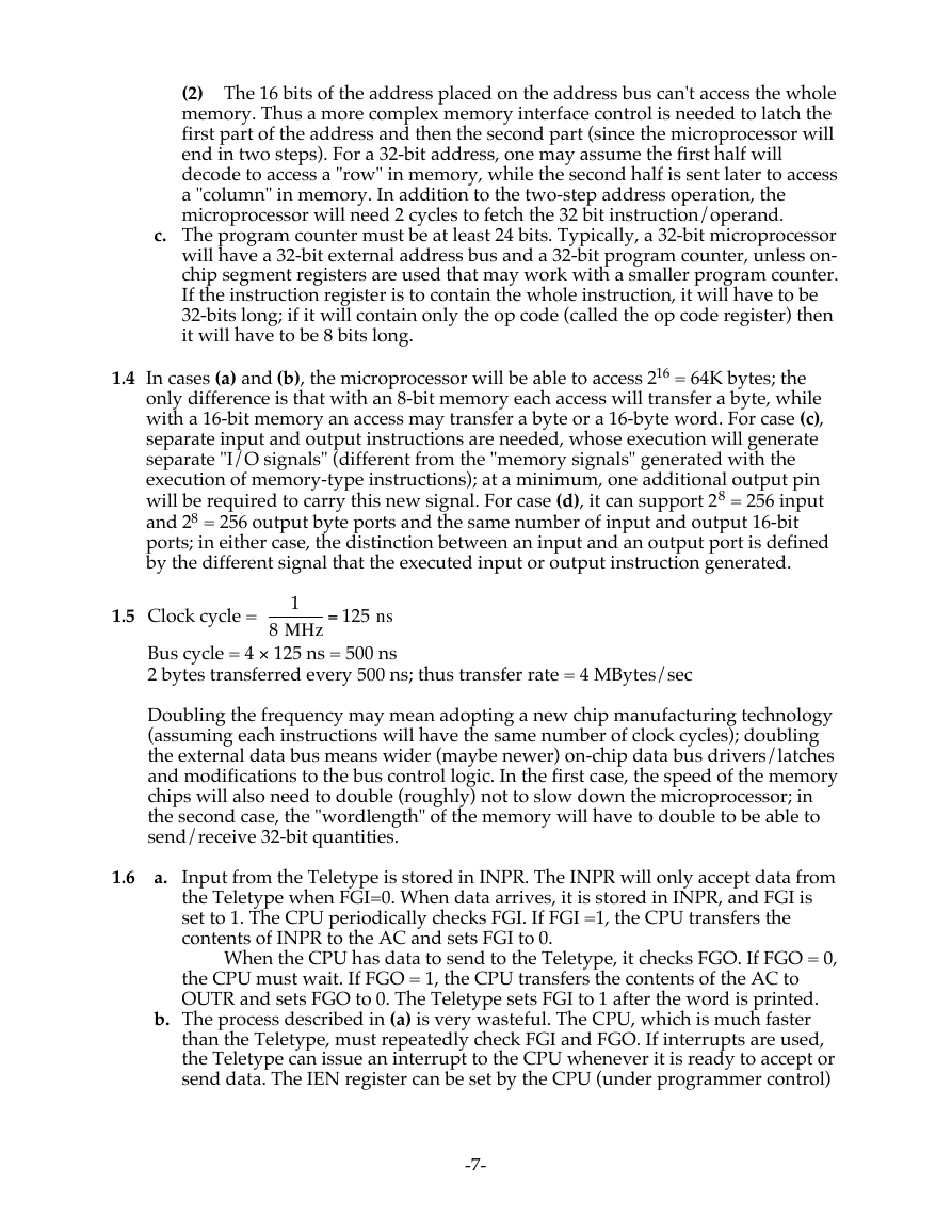
1
1.5 Clock cycle =
8 MHz = 125 ns
Bus cycle = 4 × 125 ns = 500 ns
2 bytes transferred every 500 ns; thus transfer rate = 4 MBytes/sec
Doubling the frequency may mean adopting a new chip manufacturing technology
(assuming each instructions will have the same number of clock cycles); doubling
the external data bus means wider (maybe newer) on-chip data bus drivers/latches
and modifications to the bus control logic. In the first case, the speed of the memory
chips will also need to double (roughly) not to slow down the microprocessor; in
the second case, the "wordlength" of the memory will have to double to be able to
send/receive 32-bit quantities.
a. Input from the Teletype is stored in INPR. The INPR will only accept data from
1.6
When the CPU has data to send to the Teletype, it checks FGO. If FGO = 0,
the Teletype when FGI=0. When data arrives, it is stored in INPR, and FGI is
set to 1. The CPU periodically checks FGI. If FGI =1, the CPU transfers the
contents of INPR to the AC and sets FGI to 0.
the CPU must wait. If FGO = 1, the CPU transfers the contents of the AC to
OUTR and sets FGO to 0. The Teletype sets FGI to 1 after the word is printed.
b. The process described in (a) is very wasteful. The CPU, which is much faster
than the Teletype, must repeatedly check FGI and FGO. If interrupts are used,
the Teletype can issue an interrupt to the CPU whenever it is ready to accept or
send data. The IEN register can be set by the CPU (under programmer control)
-7-
�
1.7 If a processor is held up in attempting to read or write memory, usually no damage
occurs except a slight loss of time. However, a DMA transfer may be to or from a
device that is receiving or sending data in a stream (e.g., disk or tape), and cannot
be stopped. Thus, if the DMA module is held up (denied continuing access to main
memory), data will be lost.
1.8 Let us ignore data read/write operations and assume the processor only fetches
instructions. Then the processor needs access to main memory once every
microsecond. The DMA module is transferring characters at a rate of 1200
characters per second, or one every 833 µs. The DMA therefore "steals" every 833rd
1
cycle. This slows down the processor approximately
833 ×100% = 0.12%
1.9
a. The processor can only devote 5% of its time to I/O. Thus the maximum I/O
instruction execution rate is 106 × 0.05 = 50,000 instructions per second. The I/O
transfer rate is therefore 25,000 words/second.
b. The number of machine cycles available for DMA control is
106(0.05 × 5 + 0.95 × 2) = 2.15 × 10⁶
If we assume that the DMA module can use all of these cycles, and ignore any
setup or status-checking time, then this value is the maximum I/O transfer
rate.
1.10 a. A reference to the first instruction is immediately followed by a reference to the
b. The ten accesses to a[i] within the inner for loop which occur within a short
second.
interval of time.
1.11 Define
Ci = Average cost per bit, memory level i
Si = Size of memory level i
Ti = Time to access a word in memory level i
Hi = Probability that a word is in memory i and in no higher-level memory
Bi = Time to transfer a block of data from memory level (i + 1) to memory level i
Let cache be memory level 1; main memory, memory level 2; and so on, for a total
of N levels of memory. Then
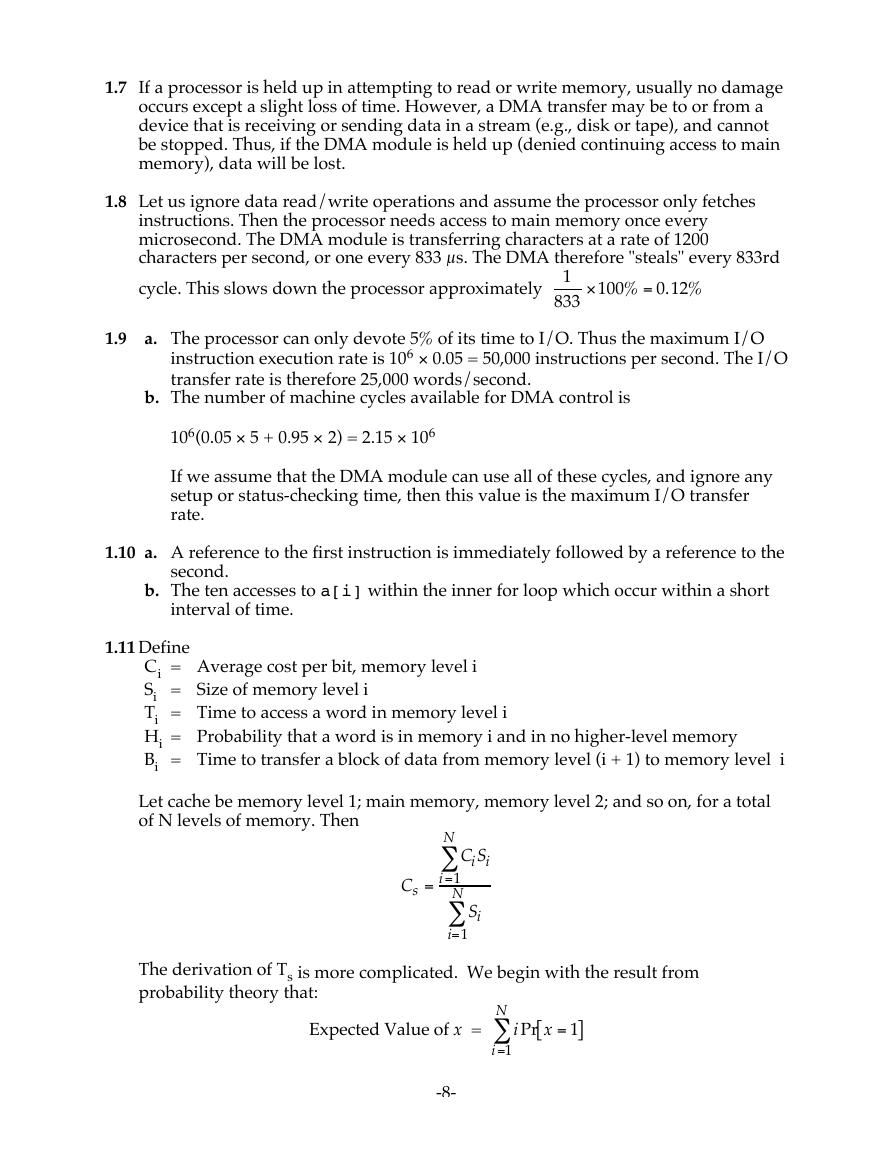
N
CiSi
∑
i =1
N
∑
i=1
Si
Cs =
The derivation of Ts is more complicated. We begin with the result from
probability theory that:
Expected Value of x =
-8-
N
∑
i =1
iPr x = 1
]
[
�


 2023年江西萍乡中考道德与法治真题及答案.doc
 2012年重庆南川中考生物真题及答案.doc
 2013年江西师范大学地理学综合及文艺理论基础考研真题.doc
 2020年四川甘孜小升初语文真题及答案I卷.doc
 2020年注册岩土工程师专业基础考试真题及答案.doc
 2023-2024学年福建省厦门市九年级上学期数学月考试题及答案.doc
 2021-2022学年辽宁省沈阳市大东区九年级上学期语文期末试题及答案.doc
 2022-2023学年北京东城区初三第一学期物理期末试卷及答案.doc
 2018上半年江西教师资格初中地理学科知识与教学能力真题及答案.doc
 2012年河北国家公务员申论考试真题及答案-省级.doc
 2020-2021学年江苏省扬州市江都区邵樊片九年级上学期数学第一次质量检测试题及答案.doc
 2022下半年黑龙江教师资格证中学综合素质真题及答案.doc