Computer Organization and Architecture
Course Design
Author:
Student Number:
Project Name: A Parallel Output Controller(POC)
Date: March 14, 2013
1
�
Contents
1 Purpose . . . . . . . . . . . . . . . . . . . . . . . . . . . . . . . . . . . . . 3
2 Tasks . . . . . . . . . . . . . . . . . . . . . . . . . . . . . . . . . . . . . . 3
3 The Overall Design Expressed in the Top Module
Form . . . . . . . . 4
3.1 Composition and Functions . . . . . . . . . . . . . . . . . . . . . . 4
3.2 Connection of the Top Level Modules . . . . . . . . . . . . . . . . 5
3.3 Block Design . . . . . . . . . . . . . . . . . . . . . . . . . . . . . . . 5
3.3.1 POC Block Design . . . . . . . . . . . . . . . . . . . . . . . 5
3.3.2 Printer Block Design . . . . . . . . . . . . . . . . . . . . . . 6
4 Design Description of the Simulation Input
Waveforms . . . . . . . . 7
5 Simulation Results . . . . . . . . . . . . . . . . . . . . . . . . . . . . . . 7
6 Conclusions and Discussions . . . . . . . . . . . . . . . . . . . . . . . .8
6.1 Conclusions . . . . . . . . . . . . . . . . . . . . . . . . . . . . . . . 8
6.2 Discussions . . . . . . . . . . . . . . . . . . . . . . . . . . . . . . . 8
Appendix . . . . . . . . . . . . . . . . . . . . . . . . . . . . . . . . . . . .9
2
�
1 Purpose
The purpose of this project is to design and simulate a parallel output
controller(POC) which acts an interface between system bus and printer.
TheAltera’s Maxplus II EDA tool is recommended and provided for
simulation.Please refer to William,Stallings.” Computer Organization
and Architecture,Designing for Performance”, P.65-75; P.185-190.
2 Tasks
POC is one of the most common I/O modules, namely the parallel output
controller. It plays the role of an interface between the computer system
bus and the peripheral (such as a printer or other output devices).
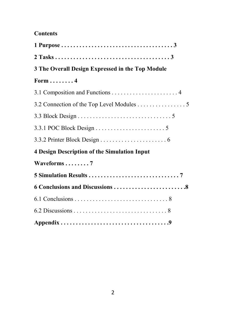
Figure 1: Printer Connection
Figure 1 shows the connecting of a printer to the system bus through the POC. The
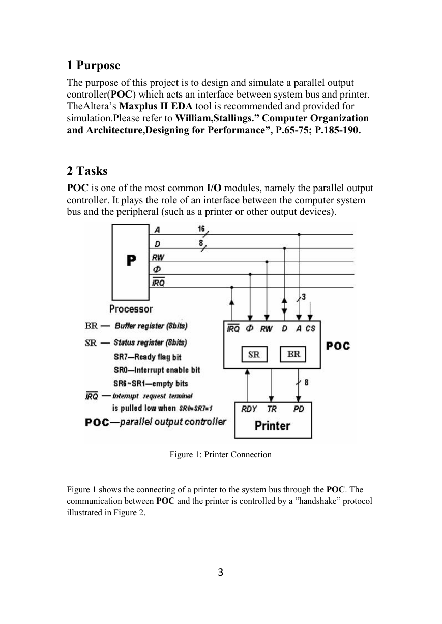
communication between POC and the printer is controlled by a ”handshake” protocol
illustrated in Figure 2.
3
�
Figure 2: The handshake-timing diagram between POC and the printer
The handshaking process is described as follows: When the printer is
ready to receive a character, it holds RDY=1.The POC must then hold a
character at PD (parallel data) port and produce a pulse at the terminal
TR (transfer request).The printer will change RDY to 0, take the
character at PD and hold the RDY at 0 until the character has been
printed (e.g. 5 or 10ms), then set RDY=1 again when it is ready to
receive the next character. (Suppose the printer has only a one
character ”buffer” register, so that each character must be printed before
the next character is sent).
3 The Overall Design Expressed in the Top Module
Form
3.1 Composition and Functions
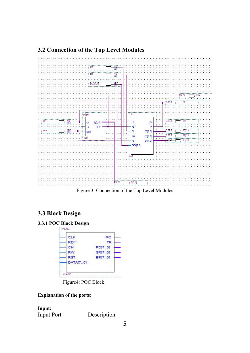
My design of the top level circuit consists of the following blocks:
POC:The parallel output controller work as the interface between the
CPU and the printer. When the printer asks for data transfer, it set SR to
sends an interrupt request signal to the CPU. Then it store the data
received from CPU in BR and generate a pulse signal TR to the printer.
Finally it transfer the data to the printer and wait for the next request.
Printer:The printer is also virtual for simulation. It generates the RDY
signal in cycle to the POC using a down counting counter 74193.
4
�
3.2 Connection of the Top Level Modules
Figure 3: Connection of the Top Level Modules
3.3 Block Design
3.3.1 POC Block Design
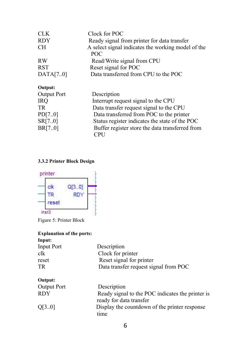
Figure4: POC Block
Explanation of the ports:
Input:
Input Port
Description
5
�
CLK
RDY
CH
RW
RST
DATA[7..0]
Output:
Output Port
IRQ
TR
PD[7..0]
SR[7..0]
BR[7..0]
Clock for POC
Ready signal from printer for data transfer
A select signal indicates the working model of the
POC
Read/Write signal from CPU
Reset signal for POC
Data transferred from CPU to the POC
Description
Interrupt request signal to the CPU
Data transfer request signal to the CPU
Data transferred from POC to the printer
Status register indicates the state of the POC
Buffer register store the data transferred from
CPU
3.3.2 Printer Block Design
Figure 5: Printer Block
Explanation of the ports:
Input:
Input Port
clk
reset
TR
Output:
Output Port
RDY
Q[3..0]
Description
Clock for printer
Reset signal for printer
Data transfer request signal from POC
Description
Ready signal to the POC indicates the printer is
ready for data transfer
Display the countdown of the printer response
time
6
�
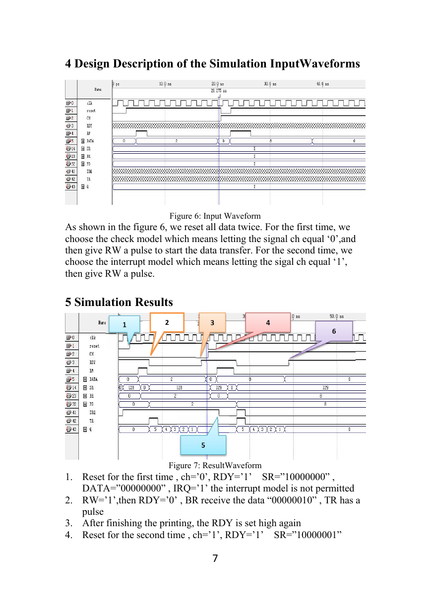
4 Design Description of the Simulation InputWaveforms
Figure 6: Input Waveform
As shown in the figure 6, we reset all data twice. For the first time, we
choose the check model which means letting the signal ch equal ‘0’,and
then give RW a pulse to start the data transfer. For the second time, we
choose the interrupt model which means letting the sigal ch equal ‘1’,
then give RW a pulse.
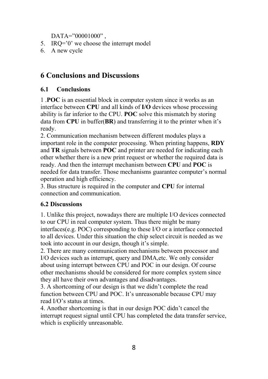
5 Simulation Results
2
Figure 7: ResultWaveform
1. Reset for the first time , ch=’0’, RDY=’1’ SR=”10000000” ,
DATA=”00000000” , IRQ=’1’ the interrupt model is not permitted
2. RW=’1’,then RDY=’0’ , BR receive the data “00000010” , TR has a
pulse
3. After finishing the printing, the RDY is set high again
4. Reset for the second time , ch=’1’, RDY=’1’ SR=”10000001”
7
�
DATA=”00001000” ,
IRQ=’0’ we choose the interrupt model
5.
6. A new cycle
6 Conclusions and Discussions
6.1 Conclusions
1 .POC is an essential block in computer system since it works as an
interface between CPU and all kinds of I/O devices whose processing
ability is far inferior to the CPU. POC solve this mismatch by storing
data from CPU in buffer(BR) and transferring it to the printer when it’s
ready.
2. Communication mechanism between different modules plays a
important role in the computer processing. When printing happens, RDY
and TR signals between POC and printer are needed for indicating each
other whether there is a new print request or whether the required data is
ready. And then the interrupt mechanism between CPU and POC is
needed for data transfer. Those mechanisms guarantee computer’s normal
operation and high efficiency.
3. Bus structure is required in the computer and CPU for internal
connection and communication.
6.2 Discussions
1. Unlike this project, nowadays there are multiple I/O devices connected
to our CPU in real computer system. Thus there might be many
interfaces(e.g. POC) corresponding to these I/O or a interface connected
to all devices. Under this situation the chip select circuit is needed as we
took into account in our design, though it’s simple.
2. There are many communication mechanisms between processor and
I/O devices such as interrupt, query and DMA,etc. We only consider
about using interrupt between CPU and POC in our design. Of course
other mechanisms should be considered for more complex system since
they all have their own advantages and disadvantages.
3. A shortcoming of our design is that we didn’t complete the read
function between CPU and POC. It’s unreasonable because CPU may
read I/O’s status at times.
4. Another shortcoming is that in our design POC didn’t cancel the
interrupt request signal until CPU has completed the data transfer service,
which is explicitly unreasonable.
8
�


 2023年江西萍乡中考道德与法治真题及答案.doc
 2012年重庆南川中考生物真题及答案.doc
 2013年江西师范大学地理学综合及文艺理论基础考研真题.doc
 2020年四川甘孜小升初语文真题及答案I卷.doc
 2020年注册岩土工程师专业基础考试真题及答案.doc
 2023-2024学年福建省厦门市九年级上学期数学月考试题及答案.doc
 2021-2022学年辽宁省沈阳市大东区九年级上学期语文期末试题及答案.doc
 2022-2023学年北京东城区初三第一学期物理期末试卷及答案.doc
 2018上半年江西教师资格初中地理学科知识与教学能力真题及答案.doc
 2012年河北国家公务员申论考试真题及答案-省级.doc
 2020-2021学年江苏省扬州市江都区邵樊片九年级上学期数学第一次质量检测试题及答案.doc
 2022下半年黑龙江教师资格证中学综合素质真题及答案.doc