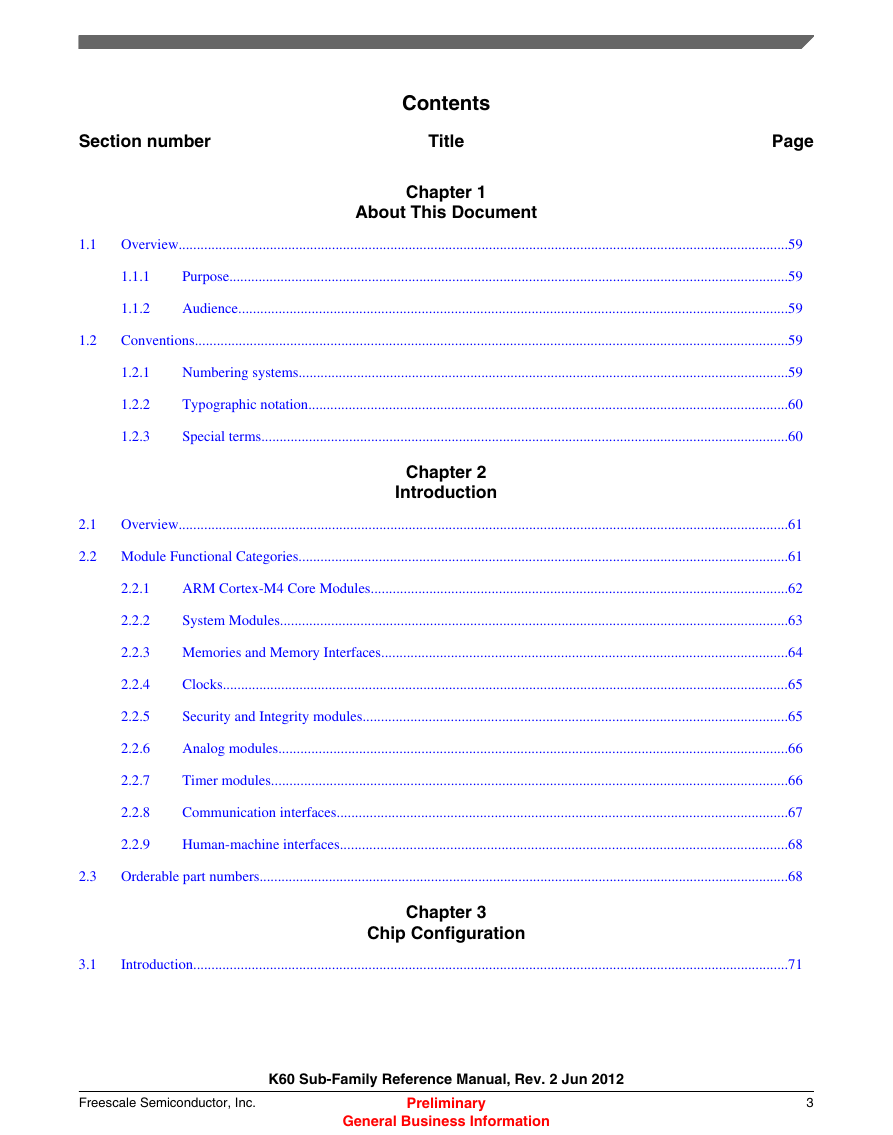
Chapter 1: About This Document
Overview
Purpose
Audience
Conventions
Numbering systems
Typographic notation
Special terms
Chapter 2: Introduction
Overview
Module Functional Categories
ARM Cortex-M4 Core Modules
System Modules
Memories and Memory Interfaces
Clocks
Security and Integrity modules
Analog modules
Timer modules
Communication interfaces
Human-machine interfaces
Orderable part numbers
Chapter 3: Chip Configuration
Introduction
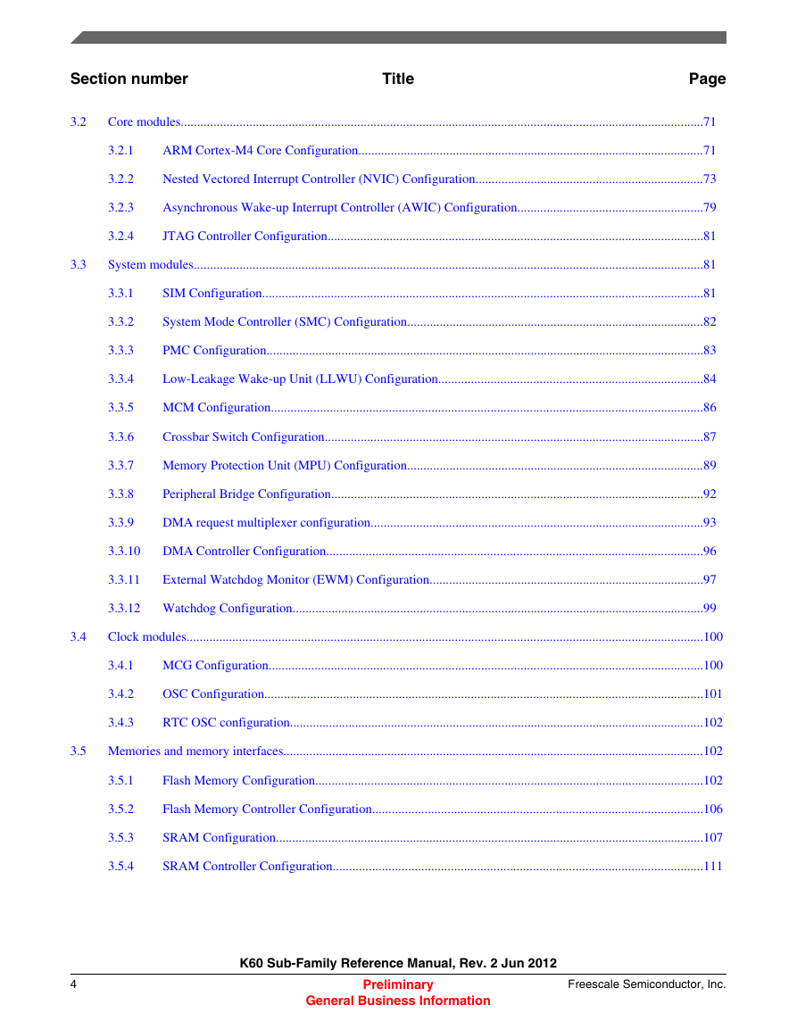
Core modules
ARM Cortex-M4 Core Configuration
Buses, interconnects, and interfaces
System Tick Timer
Debug facilities
Core privilege levels
Nested Vectored Interrupt Controller (NVIC) Configuration
Interrupt priority levels
Non-maskable interrupt
Interrupt channel assignments
Determining the bitfield and register location for configuring a particular interrupt
Asynchronous Wake-up Interrupt Controller (AWIC) Configuration
Wake-up sources
JTAG Controller Configuration
System modules
SIM Configuration
System Mode Controller (SMC) Configuration
PMC Configuration
Low-Leakage Wake-up Unit (LLWU) Configuration
Wake-up Sources
MCM Configuration
Crossbar Switch Configuration
Crossbar Switch Master Assignments
Crossbar Switch Slave Assignments
PRS register reset values
Memory Protection Unit (MPU) Configuration
MPU Slave Port Assignments
MPU Logical Bus Master Assignments
MPU Access Violation Indications
Reset Values for RGD0 Registers
Write Access Restrictions for RGD0 Registers
Peripheral Bridge Configuration
Number of peripheral bridges
Memory maps
MPRA register
AIPS_Lite MPRA register reset value
PACR registers
AIPS_Lite PACRE-P register reset values
DMA request multiplexer configuration
DMA MUX request sources
DMA transfers via PIT trigger
DMA Controller Configuration
External Watchdog Monitor (EWM) Configuration
EWM clocks
EWM low-power modes
EWM_OUT pin state in low power modes
Watchdog Configuration
WDOG clocks
WDOG low-power modes
Clock modules
MCG Configuration
OSC Configuration
OSC modes of operation with MCG
RTC OSC configuration
Memories and memory interfaces
Flash Memory Configuration
Flash memory types
Flash Memory Sizes
Flash Memory Size Considerations
Flash Memory Map
Flash Security
Flash Modes
Erase All Flash Contents
FTFL_FOPT Register
Flash Memory Controller Configuration
Number of masters
Program Flash Swap
SRAM Configuration
SRAM sizes
SRAM Arrays
SRAM retention in low power modes
SRAM accesses
SRAM arbitration and priority control
SRAM Controller Configuration
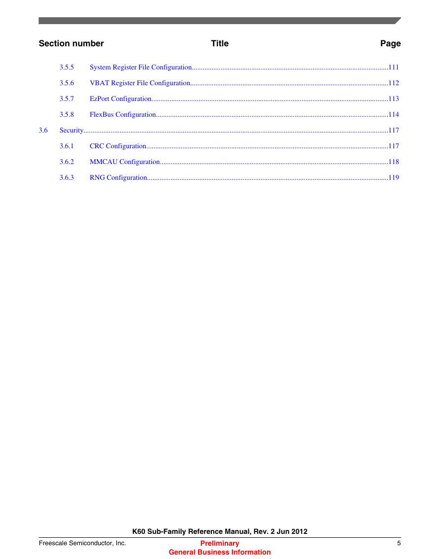
System Register File Configuration
System Register file
VBAT Register File Configuration
VBAT register file
EzPort Configuration
JTAG instruction
Flash Option Register (FOPT)
FlexBus Configuration
FlexBus clocking
FlexBus signal multiplexing
FlexBus CSCR0 reset value
FlexBus Security
FlexBus line transfers
Security
CRC Configuration
MMCAU Configuration
RNG Configuration
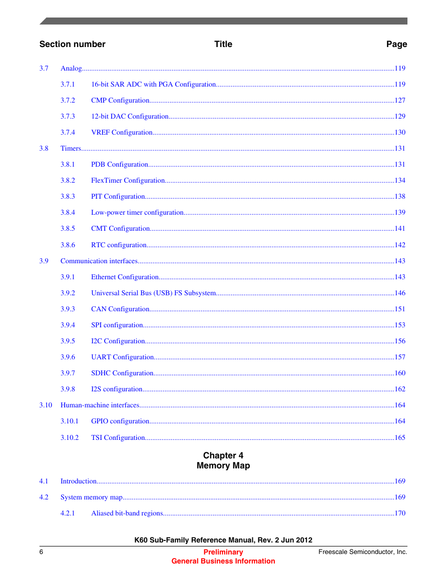
Analog
16-bit SAR ADC with PGA Configuration
ADC instantiation information
DMA Support on ADC
Connections/channel assignment
ADC0 Connections/Channel Assignment
ADC1 Connections/Channel Assignment
ADC Channels MUX Selection
ADC Hardware Interleaved Channels
ADC and PGA Reference Options
ADC triggers
Alternate clock
ADC low-power modes
PGA Integration
CMP Configuration
CMP input connections
CMP external references
External window/sample input
12-bit DAC Configuration
12-bit DAC Overview
12-bit DAC Output
12-bit DAC Reference
VREF Configuration
VREF Overview
Timers
PDB Configuration
PDB Instantiation
PDB Module Interconnections
Back-to-back acknowledgement connections
PDB Interval Trigger Connections to DAC
DAC External Trigger Input Connections
Pulse-Out Connection
Pulse-Out Enable Register Implementation
FlexTimer Configuration
Instantiation Information
External Clock Options
Fixed frequency clock
FTM Interrupts
FTM Fault Detection Inputs
FTM Hardware Triggers
Input capture options for FTM module instances
FTM output triggers for other modules
FTM Global Time Base
FTM BDM and debug halt mode
PIT Configuration
PIT/DMA Periodic Trigger Assignments
PIT/ADC Triggers
Low-power timer configuration
LPTMR prescaler/glitch filter clocking options
LPTMR pulse counter input options
CMT Configuration
Instantiation Information
IRO Drive Strength
RTC configuration
RTC_CLKOUT signal
Communication interfaces
Ethernet Configuration
Ethernet Clocking Options
RMII Clocking
IEEE 1588 Timers
Ethernet Operation in Low Power Modes
Ethernet Doze Mode
Ethernet Interrupts
Ethernet event signal
Universal Serial Bus (USB) FS Subsystem
USB Wakeup
USB Power Distribution
USB power management
USB controller configuration
USB DCD Configuration
USB Voltage Regulator Configuration
CAN Configuration
Number of FlexCAN modules
Reset value of MDIS bit
Number of message buffers
FlexCAN Clocking
FlexCAN Interrupts
FlexCAN Operation in Low Power Modes
FlexCAN Doze Mode
SPI configuration
SPI Modules Configuration
SPI clocking
Number of CTARs
TX FIFO size
RX FIFO Size
Number of PCS signals
SPI Operation in Low Power Modes
Using GPIO Interrupt to Wake from stop mode
SPI Doze Mode
SPI Interrupts
SPI clocks
I2C Configuration
Number of I2C modules
UART Configuration
UART configuration information
UART wakeup
UART interrupts
SDHC Configuration
SDHC clocking
SD bus pullup/pulldown constraints
I2S configuration
Instantiation information
I2S/SAI clocking
I2S/SAI operation in low power modes
Human-machine interfaces
GPIO configuration
GPIO access protection
Number of GPIO signals
TSI Configuration
Number of inputs
TSI module functionality in MCU operation modes
TSI clocks
TSI Interrupts
Shield drive signal
Chapter 4: Memory Map
Introduction
System memory map
Aliased bit-band regions
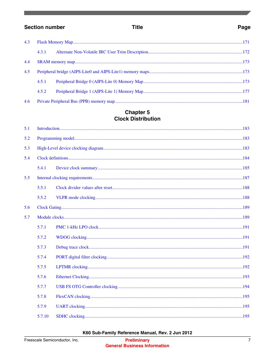
Flash Memory Map
Alternate Non-Volatile IRC User Trim Description
SRAM memory map
Peripheral bridge (AIPS-Lite0 and AIPS-Lite1) memory maps
Peripheral Bridge 0 (AIPS-Lite 0) Memory Map
Peripheral Bridge 1 (AIPS-Lite 1) Memory Map
Private Peripheral Bus (PPB) memory map
Chapter 5: Clock Distribution
Introduction
Programming model
High-Level device clocking diagram
Clock definitions
Device clock summary
Internal clocking requirements
Clock divider values after reset
VLPR mode clocking
Clock Gating
Module clocks
PMC 1-kHz LPO clock
WDOG clocking
Debug trace clock
PORT digital filter clocking
LPTMR clocking
Ethernet Clocking
USB FS OTG Controller clocking
FlexCAN clocking
UART clocking
SDHC clocking
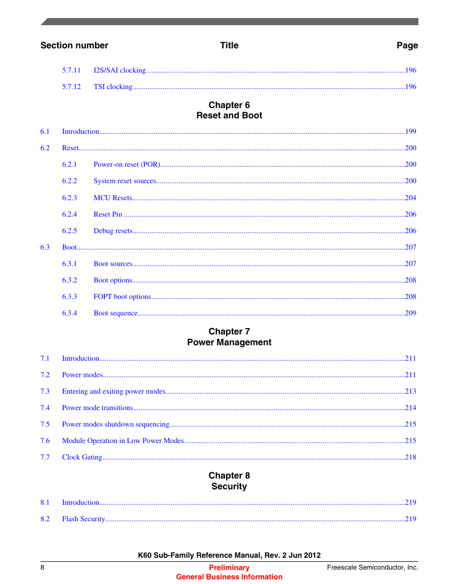
I2S/SAI clocking
TSI clocking
Chapter 6: Reset and Boot
Introduction
Reset
Power-on reset (POR)
System reset sources
External pin reset (PIN)
Reset pin filter
Low-voltage detect (LVD)
Computer operating properly (COP) watchdog timer
Low leakage wakeup (LLWU)
Multipurpose clock generator loss-of-clock (LOC)
MCG loss-of-lock (LOL) reset
Stop mode acknowledge error (SACKERR)
Software reset (SW)
Lockup reset (LOCKUP)
EzPort reset
MDM-AP system reset request
MCU Resets
Reset Pin
Debug resets
JTAG reset
nTRST reset
Resetting the Debug subsystem
Boot
Boot sources
Boot options
FOPT boot options
Boot sequence
Chapter 7: Power Management
Introduction
Power modes
Entering and exiting power modes
Power mode transitions
Power modes shutdown sequencing
Module Operation in Low Power Modes
Clock Gating
Chapter 8: Security
Introduction
Flash Security
Security Interactions with other Modules
Security interactions with FlexBus
Security Interactions with EzPort
Security Interactions with Debug
Chapter 9: Debug
Introduction
References
The Debug Port
Debug Port Pin Descriptions
System TAP connection
JTAG status and control registers
MDM-AP Control Register
MDM-AP Status Register
Debug Resets
AHB-AP
ITM
Core Trace Connectivity
Embedded Trace Macrocell v3.5 (ETM)
Coresight Embedded Trace Buffer (ETB)
TPIU
DWT
Debug in Low Power Modes
Debug & Security
Chapter 10: Signal Multiplexing and Signal Descriptions
Introduction
Signal Multiplexing Integration
Port control and interrupt module features
PCRn reset values for port A
Clock gating
Signal multiplexing constraints
Pinout
K60 Signal Multiplexing and Pin Assignments
K60 Pinouts
Module Signal Description Tables
Core Modules
System Modules
Clock Modules
Memories and Memory Interfaces
Analog
Timer Modules
Communication Interfaces
Human-Machine Interfaces (HMI)
Chapter 11: Port control and interrupts (PORT)
Introduction
Overview
Features
Modes of operation
Run mode
Wait mode
Stop mode
Debug mode
External signal description
Detailed signal description
Memory map and register definition
PORTx
PORTx_PCRn
PORTx_GPCLR
PORTx_GPCHR
PORTx_ISFR
Functional description
Pin control
Global pin control
External interrupts
Chapter 12: System Integration Module (SIM)
Introduction
Features
Memory map and register definition
SIM
SIM_SOPT1
SIM_SOPT1CFG
SIM_SOPT2
SIM_SOPT4
SIM_SOPT5
SIM_SOPT7
SIM_SDID
SIM_SCGC1
SIM_SCGC2
SIM_SCGC3
SIM_SCGC4
SIM_SCGC5
SIM_SCGC6
SIM_SCGC7
SIM_CLKDIV1
SIM_CLKDIV2
SIM_FCFG1
SIM_FCFG2
SIM_UIDH
SIM_UIDMH
SIM_UIDML
SIM_UIDL
Functional description
Chapter 13: Reset Control Module (RCM)
Introduction
Reset memory map and register descriptions
RCM
RCM_SRS0
RCM_SRS1
RCM_RPFC
RCM_RPFW
RCM_MR
Chapter 14: System Mode Controller
Introduction
Modes of operation
Memory map and register descriptions
SMC
SMC_PMPROT
SMC_PMCTRL
SMC_VLLSCTRL
SMC_PMSTAT
Functional description
Power mode transitions
Power mode entry/exit sequencing
Stop mode entry sequence
Stop mode exit sequence
Aborted stop mode entry
Transition to wait modes
Transition from stop modes to Debug mode
Run modes
RUN mode
Very-Low Power Run (VLPR) mode
Wait modes
WAIT mode
Very-Low-Power Wait (VLPW) mode
Stop modes
STOP mode
Very-Low-Power Stop (VLPS) mode
Low-Leakage Stop (LLS) mode
Very-Low-Leakage Stop (VLLSx) modes
Debug in low power modes
Chapter 15: Power Management Controller
Introduction
Features
Low-voltage detect (LVD) system
LVD reset operation
LVD interrupt operation
Low-voltage warning (LVW) interrupt operation
I/O retention
Memory map and register descriptions
PMC
PMC_LVDSC1
PMC_LVDSC2
PMC_REGSC
Chapter 16: Low-Leakage Wakeup Unit (LLWU)
Introduction
Features
Modes of operation
LLS mode
VLLS modes
Non-low leakage modes
Debug mode
Block diagram
LLWU signal descriptions
Memory map/register definition
LLWU
LLWU_PE1
LLWU_PE2
LLWU_PE3
LLWU_PE4
LLWU_ME
LLWU_F1
LLWU_F2
LLWU_F3
LLWU_FILT1
LLWU_FILT2
LLWU_RST
Functional description
LLS mode
VLLS modes
Initialization
Chapter 17: Miscellaneous Control Module (MCM)
Introduction
Features
Memory map/register descriptions
MCM
MCM_PLASC
MCM_PLAMC
MCM_CR
MCM_ISR
MCM_ETBCC
MCM_ETBRL
MCM_ETBCNT
MCM_PID
Functional description
Interrupts
Chapter 18: Crossbar Switch (AXBS)
Introduction
Features
Memory Map / Register Definition
AXBS
AXBS_PRSn
AXBS_CRSn
AXBS_MGPCRn
Functional Description
General operation
Register coherency
Arbitration
Arbitration during undefined length bursts
Fixed-priority operation
Round-robin priority operation
Priority assignment
Initialization/application information
Chapter 19: Memory Protection Unit (MPU)
Introduction
Overview
Block diagram
Features
Memory map/register definition
MPU
MPU_CESR
MPU_EARn
MPU_EDRn
MPU_RGDn_WORD0
MPU_RGDn_WORD1
MPU_RGDn_WORD2
MPU_RGDn_WORD3
MPU_RGDAACn
Functional description
Access evaluation macro
Hit determination
Privilege violation determination
Putting it all together and error terminations
Power management
Initialization information
Application information
Chapter 20: Peripheral Bridge (AIPS-Lite)
Introduction
Features
General operation
Memory map/register definition
AIPSx
AIPSx_MPRA
AIPSx_PACRn
AIPSx_PACRn
Functional description
Access support
Chapter 21: Direct Memory Access Multiplexer (DMAMUX)
Introduction
Overview
Features
Modes of operation
External signal description
Memory map/register definition
DMAMUX
DMAMUX_CHCFGn
Functional description
DMA channels with periodic triggering capability
DMA channels with no triggering capability
"Always enabled" DMA sources
Initialization/application information
Reset
Enabling and configuring sources
Chapter 22: Direct Memory Access Controller (eDMA)
Introduction
Block diagram
Block parts
Features
Modes of operation
Memory map/register definition
DMA
DMA_CR
DMA_ES
DMA_ ERQ
DMA_ EEI
DMA_CEEI
DMA_SEEI
DMA_CERQ
DMA_SERQ
DMA_CDNE
DMA_SSRT
DMA_CERR
DMA_CINT
DMA_ INT
DMA_ ERR
DMA_ HRS
DMA_DCHPRIn
DMA_TCDn_SADDR
DMA_TCDn_SOFF
DMA_TCDn_ATTR
DMA_TCDn_NBYTES_MLNO
DMA_TCDn_NBYTES_MLOFFNO
DMA_TCDn_NBYTES_MLOFFYES
DMA_TCDn_SLAST
DMA_TCDn_DADDR
DMA_TCDn_DOFF
DMA_TCDn_CITER_ELINKYES
DMA_TCDn_CITER_ELINKNO
DMA_TCDn_DLASTSGA
DMA_TCDn_CSR
DMA_TCDn_BITER_ELINKYES
DMA_TCDn_BITER_ELINKNO
Functional description
eDMA basic data flow
Error reporting and handling
Channel preemption
Performance
Initialization/application information
eDMA initialization
Programming errors
Arbitration mode considerations
Fixed channel arbitration
Round-robin channel arbitration
Performing DMA transfers (examples)
Single request
Multiple requests
Using the modulo feature
Monitoring transfer descriptor status
Testing for minor loop completion
Reading the transfer descriptors of active channels
Checking channel preemption status
Channel Linking
Dynamic programming
Dynamically changing the channel priority
Dynamic channel linking
Dynamic scatter/gather
Method 1 (channel not using major loop channel linking)
Method 2 (channel using major loop channel linking)
Chapter 23: External Watchdog Monitor (EWM)
Introduction
Features
Modes of Operation
Stop Mode
Wait Mode
Debug Mode
Block Diagram
EWM Signal Descriptions
Memory Map/Register Definition
EWM
EWM_CTRL
EWM_SERV
EWM_CMPL
EWM_CMPH
EWM_CLKPRESCALER
Functional Description
The EWM_out Signal
The EWM_in Signal
EWM Counter
EWM Compare Registers
EWM Refresh Mechanism
EWM Interrupt
Counter clock prescaler
Chapter 24: Watchdog Timer (WDOG)
Introduction
Features
Functional overview
Unlocking and updating the watchdog
Watchdog configuration time (WCT)
Refreshing the watchdog
Windowed mode of operation
Watchdog disabled mode of operation
Low-power modes of operation
Debug modes of operation
Testing the watchdog
Quick test
Byte test
Backup reset generator
Generated resets and interrupts
Memory map and register definition
WDOG
WDOG_STCTRLH
WDOG_STCTRLL
WDOG_TOVALH
WDOG_TOVALL
WDOG_WINH
WDOG_WINL
WDOG_REFRESH
WDOG_UNLOCK
WDOG_TMROUTH
WDOG_TMROUTL
WDOG_RSTCNT
WDOG_PRESC
Watchdog operation with 8-bit access
General guideline
Refresh and unlock operations with 8-bit access
Restrictions on watchdog operation
Chapter 25: Multipurpose Clock Generator (MCG)
Introduction
Features
Modes of Operation
External Signal Description
Memory Map/Register Definition
MCG
MCG_C1
MCG_C2
MCG_C3
MCG_C4
MCG_C5
MCG_C6
MCG_S
MCG_SC
MCG_ATCVH
MCG_ATCVL
MCG_C7
MCG_C8
MCG_C9
MCG_C10
Functional Description
MCG mode state diagram
MCG modes of operation
MCG mode switching
Low Power Bit Usage
MCG Internal Reference Clocks
MCG Internal Reference Clock
External Reference Clock
MCG Fixed frequency clock
MCG PLL clock
MCG Auto TRIM (ATM)
Initialization / Application information
MCG module initialization sequence
Initializing the MCG
Using a 32.768 kHz reference
MCG mode switching
Example 1: Moving from FEI to PEE mode: External Crystal = 4 MHz, MCGOUTCLK frequency = 48 MHz
Example 2: Moving from PEE to BLPI mode: MCGOUTCLK frequency =32 kHz
Example 3: Moving from BLPI to FEE mode
Chapter 26: Oscillator (OSC)
Introduction
Features and Modes
Block Diagram
OSC Signal Descriptions
External Crystal / Resonator Connections
External Clock Connections
Memory Map/Register Definitions
Functional Description
OSC Module States
Off
Oscillator Start-Up
Oscillator Stable
External Clock Mode
OSC Module Modes
Low-Frequency, High-Gain Mode
Low-Frequency, Low-Power Mode
High-Frequency, High-Gain Mode
High-Frequency, Low-Power Mode
Counter
Reference Clock Pin Requirements
Reset
Low Power Modes Operation
Interrupts
Chapter 27: RTC Oscillator
Introduction
Features and Modes
Block Diagram
RTC Signal Descriptions
EXTAL32 — Oscillator Input
XTAL32 — Oscillator Output
External Crystal Connections
Memory Map/Register Descriptions
Functional Description
Reset Overview
Interrupts
Chapter 28: Flash Memory Controller (FMC)
Introduction
Overview
Features
Modes of operation
External signal description
Memory map and register descriptions
FMC
FMC_PFAPR
FMC_PFB0CR
FMC_PFB1CR
FMC_TAGVDW0Sn
FMC_TAGVDW1Sn
FMC_TAGVDW2Sn
FMC_TAGVDW3Sn
FMC_DATAW0SnU
FMC_DATAW0SnL
FMC_DATAW1SnU
FMC_DATAW1SnL
FMC_DATAW2SnU
FMC_DATAW2SnL
FMC_DATAW3SnU
FMC_DATAW3SnL
Functional description
Wait states
Speculative reads
Initialization and application information
Chapter 29: Flash Memory Module (FTFL)
Introduction
Features
Program Flash Memory Features
FlexNVM Memory Features
Programming Acceleration RAM Features
FlexRAM Features
Other Flash Memory Module Features
Block Diagram
Glossary
External Signal Description
Memory Map and Registers
Flash Configuration Field Description
Program Flash IFR Map
Program Once Field
Data Flash IFR Map
EEPROM Data Set Size
FlexNVM Partition Code
Register Descriptions
FTFL
FTFL_FSTAT
FTFL_FCNFG
FTFL_FSEC
FTFL_FOPT
FTFL_FCCOBn
FTFL_FPROTn
FTFL_FEPROT
FTFL_FDPROT
Functional Description
Program Flash Memory Swap
Flash Protection
FlexNVM Description
FlexNVM Block Partitioning for FlexRAM
EEPROM User Perspective
EEPROM Implementation Overview
Write endurance to FlexRAM for EEPROM
Interrupts
Flash Operation in Low-Power Modes
Wait Mode
Stop Mode
Functional Modes of Operation
Flash Reads and Ignored Writes
Read While Write (RWW)
Flash Program and Erase
Flash Command Operations
Command Write Sequence
Load the FCCOB Registers
Launch the Command by Clearing CCIF
Command Execution and Error Reporting
Flash Commands
Flash Commands by Mode
Allowed Simultaneous Flash Operations
Margin Read Commands
Flash Command Description
Read 1s Block Command
Read 1s Section Command
Program Check Command
Read Resource Command
Program Longword Command
Erase Flash Block Command
Erase Flash Sector Command
Suspending an Erase Flash Sector Operation
Resuming a Suspended Erase Flash Sector Operation
Aborting a Suspended Erase Flash Sector Operation
Program Section Command
Flash Sector Programming
Read 1s All Blocks Command
Read Once Command
Program Once Command
Erase All Blocks Command
Triggering an Erase All External to the Flash Memory Module
Verify Backdoor Access Key Command
Swap Control Command
Swap State Determination
Program Partition Command
Set FlexRAM Function Command
Security
Flash Memory Access by Mode and Security
Changing the Security State
Unsecuring the Chip Using Backdoor Key Access
Reset Sequence
Chapter 30: External Bus Interface (FlexBus)
Introduction
Definition
Features
Signal descriptions
Memory Map/Register Definition
FB
FB_CSARn
FB_CSMRn
FB_CSCRn
FB_CSPMCR
Functional description
Modes of operation
Address comparison
Address driven on address bus
Connecting address/data lines
Bit ordering
Data transfer signals
Signal transitions
Data-byte alignment and physical connections
Address/data bus multiplexing
FlexBus multiplexed operating modes for CSCRn[BLS]=0
FlexBus multiplexed operating modes for CSCRn[BLS]=1
Data transfer states
FlexBus Timing Examples
Basic Read Bus Cycle
Basic Write Bus Cycle
Bus Cycle Sizing
Bus Cycle Sizing—Byte Transfer, 8-bit Device, No Wait States
Bus Cycle Sizing—Word Transfer, 16-bit Device, No Wait States
Bus Cycle Sizing—Longword Transfer, 32-bit Device, No Wait States
Timing Variations
Wait States
Address Setup and Hold
Burst cycles
Enabling and inhibiting burst
Transfer size and port size translation
32-bit-Read burst from 8-Bit port 2-1-1-1 (no wait states)
32-bit-Write burst to 8-Bit port 3-1-1-1 (no wait states)
32-bit-write burst-inhibited to 8-bit port (no wait states)
32-bit-read burst from 8-bit port 3-2-2-2 (one wait state)
32-bit-write burst to 8-bit port 3-2-2-2 (one wait state)
32-bit-read burst from 8-bit port 3-1-1-1 (address setup and hold)
32-bit-write burst to 8-bit port 3-1-1-1 (address setup and hold)
Extended Transfer Start/Address Latch Enable
Bus errors
Initialization/Application Information
Initializing a chip-select
Reconfiguring a chip-select
Chapter 31: EzPort
Overview
Introduction
Features
Modes of operation
External signal description
EzPort Clock (EZP_CK)
EzPort Chip Select (EZP_CS)
EzPort Serial Data In (EZP_D)
EzPort Serial Data Out (EZP_Q)
Command definition
Command descriptions
Write Enable
Write Disable
Read Status Register
Read Data
Read Data at High Speed
Section Program
Sector Erase
Bulk Erase
EzPort Reset Chip
Write FCCOB Registers
Read FCCOB Registers at High Speed
Write FlexRAM
Read FlexRAM
Read FlexRAM at High Speed
Flash memory map for EzPort access
Chapter 32: Cyclic Redundancy Check (CRC)
Introduction
Features
Block diagram
Modes of operation
Run mode
Low-power modes (Wait or Stop)
Memory map and register descriptions
CRC
CRC_CRC
CRC_GPOLY
CRC_CTRL
Functional description
CRC initialization/reinitialization
CRC calculations
16-bit CRC
32-bit CRC
Transpose feature
Types of transpose
CRC result complement
Chapter 33: Memory-Mapped Cryptographic Acceleration Unit (MMCAU)
Introduction
MMCAU Block Diagram
Overview
Features
Memory map/register definition
CAU
CAU_CASR
CAU_CAA
CAU_CAn
Functional description
MMCAU programming model
Direct loads
Indirect loads
Indirect stores
MMCAU integrity checks
Address integrity checks
Data integrity checks
CAU commands
Coprocessor No Operation (CNOP)
Load Register (LDR)
Store Register (STR)
Add to Register (ADR)
Reverse and Add to Register (RADR)
Add Register to Accumulator (ADRA)
Exclusive Or (XOR)
Rotate Left (ROTL)
Move Register to Accumulator (MVRA)
Move Accumulator to Register (MVAR)
AES Substitution (AESS)
AES Inverse Substitution (AESIS)
AES Column Operation (AESC)
AES Inverse Column Operation (AESIC)
AES Shift Rows (AESR)
AES Inverse Shift Rows (AESIR)
DES Round (DESR)
DES Key setup (DESK)
Hash Function (HASH)
Secure Hash Shift (SHS)
Message Digest Shift (MDS)
Secure Hash Shift 2 (SHS2)
Illegal command (ILL)
Application/initialization information
Code example
Assembler equate values
Chapter 34: Random Number Generator Accelerator (RNGA)
Introduction
Overview
Modes of operation
Memory map and register definition
RNG
RNG_CR
RNG_SR
RNG_ER
RNG_OR
Functional description
RNGA Output Register
RNGA Core/Control Logic Block
RNGA Control Block
Core Engine
Initialization/application information
Chapter 35: Analog-to-Digital Converter (ADC)
Introduction
Features
Block diagram
ADC Signal Descriptions
Analog Power (VDDA)
Analog Ground (VSSA)
Voltage Reference Select
Analog Channel Inputs (ADx)
Differential Analog Channel Inputs (DADx)
Register definition
ADCx
ADCx_SC1n
ADCx_CFG1
ADCx_CFG2
ADCx_Rn
ADCx_CVn
ADCx_SC2
ADCx_SC3
ADCx_OFS
ADCx_PG
ADCx_MG
ADCx_CLPD
ADCx_CLPS
ADCx_CLP4
ADCx_CLP3
ADCx_CLP2
ADCx_CLP1
ADCx_CLP0
ADCx_PGA
ADCx_CLMD
ADCx_CLMS
ADCx_CLM4
ADCx_CLM3
ADCx_CLM2
ADCx_CLM1
ADCx_CLM0
Functional description
PGA functional description
Clock select and divide control
Voltage reference selection
Hardware trigger and channel selects
Conversion control
Initiating conversions
Completing conversions
Aborting conversions
Power control
Sample time and total conversion time
Conversion time examples
Typical conversion time configuration
Long conversion time configuration
Short conversion time configuration
Hardware average function
Automatic compare function
Calibration function
User-defined offset function
Temperature sensor
MCU wait mode operation
MCU Normal Stop mode operation
Normal Stop mode with ADACK disabled
Normal Stop mode with ADACK enabled
MCU Low-Power Stop mode operation
Initialization information
ADC module initialization example
Initialization sequence
Pseudo-code example
Application information
External pins and routing
Analog supply pins
Analog voltage reference pins
Analog input pins
Sources of error
Sampling error
Pin leakage error
Noise-induced errors
Code width and quantization error
Linearity errors
Code jitter, non-monotonicity, and missing codes
Chapter 36: Comparator (CMP)
Introduction
CMP features
6-bit DAC key features
ANMUX key features
CMP, DAC and ANMUX diagram
CMP block diagram
Memory map/register definitions
CMPx
CMPx_CR0
CMPx_CR1
CMPx_FPR
CMPx_SCR
CMPx_DACCR
CMPx_MUXCR
CMP functional description
CMP functional modes
Disabled mode (# 1)
Continuous mode (#s 2A & 2B)
Sampled, Non-Filtered mode (#s 3A & 3B)
Sampled, Filtered mode (#s 4A & 4B)
Windowed mode (#s 5A & 5B)
Windowed/Resampled mode (# 6)
Windowed/Filtered mode (#7)
Power modes
Wait mode operation
Stop mode operation
Low-Leakage mode operation
Startup and operation
Low-pass filter
Enabling filter modes
Latency issues
CMP interrupts
CMP DMA support
Digital-to-analog converter block diagram
DAC functional description
Voltage reference source select
DAC resets
DAC clocks
DAC interrupts
Chapter 37: 12-bit Digital-to-Analog Converter (DAC)
Introduction
Features
Block diagram
Memory map/register definition
DACx
DACx_DATnL
DACx_DATnH
DACx_SR
DACx_C0
DACx_C1
DACx_C2
Functional description
DAC data buffer operation
DAC data buffer interrupts
Modes of DAC data buffer operation
DMA operation
Resets
Low-Power mode operation
Chapter 38: Voltage Reference (VREFV1)
Introduction
Overview
Features
Modes of Operation
VREF Signal Descriptions
Memory Map and Register Definition
VREF
VREF_TRM
VREF_SC
Functional Description
Voltage Reference Disabled, SC[VREFEN] = 0
Voltage Reference Enabled, SC[VREFEN] = 1
SC[MODE_LV]=00
SC[MODE_LV] = 01
SC[MODE_LV] = 10
SC[MODE_LV] = 11
Initialization/Application Information
Chapter 39: Programmable Delay Block (PDB)
Introduction
Features
Implementation
Back-to-back acknowledgment connections
DAC External Trigger Input Connections
Block diagram
Modes of operation
PDB signal descriptions
Memory map and register definition
PDBx
PDBx_SC
PDBx_MOD
PDBx_CNT
PDBx_IDLY
PDBx_CHnC1
PDBx_CHnS
PDBx_CHnDLY0
PDBx_CHnDLY1
PDBx_DACINTCn
PDBx_DACINTn
PDBx_POEN
PDBx_POnDLY
Functional description
PDB pre-trigger and trigger outputs
PDB trigger input source selection
DAC interval trigger outputs
Pulse-Out's
Updating the delay registers
Interrupts
DMA
Application information
Impact of using the prescaler and multiplication factor on timing resolution
Chapter 40: FlexTimer Module (FTM)
Introduction
FlexTimer philosophy
Features
Modes of operation
Block diagram
FTM signal descriptions
Memory map and register definition
Memory map
Register descriptions
FTMx
FTMx_SC
FTMx_CNT
FTMx_MOD
FTMx_CnSC
FTMx_CnV
FTMx_CNTIN
FTMx_STATUS
FTMx_MODE
FTMx_SYNC
FTMx_OUTINIT
FTMx_OUTMASK
FTMx_COMBINE
FTMx_DEADTIME
FTMx_EXTTRIG
FTMx_POL
FTMx_FMS
FTMx_FILTER
FTMx_FLTCTRL
FTMx_QDCTRL
FTMx_CONF
FTMx_FLTPOL
FTMx_SYNCONF
FTMx_INVCTRL
FTMx_SWOCTRL
FTMx_PWMLOAD
Functional description
Clock source
Counter clock source
Prescaler
Counter
Up counting
Up-down counting
Free running counter
Counter reset
When the TOF bit is set
Input Capture mode
Filter for Input Capture mode
Output Compare mode
Edge-Aligned PWM (EPWM) mode
Center-Aligned PWM (CPWM) mode
Combine mode
Asymmetrical PWM
Complementary mode
Registers updated from write buffers
CNTIN register update
MOD register update
CnV register update
PWM synchronization
Hardware trigger
Software trigger
Boundary cycle and loading points
MOD register synchronization
CNTIN register synchronization
C(n)V and C(n+1)V register synchronization
OUTMASK register synchronization
INVCTRL register synchronization
SWOCTRL register synchronization
FTM counter synchronization
Inverting
Software output control
Deadtime insertion
Deadtime insertion corner cases
Output mask
Fault control
Automatic fault clearing
Manual fault clearing
Fault inputs polarity control
Polarity control
Initialization
Features priority
Channel trigger output
Initialization trigger
Capture Test mode
DMA
Dual Edge Capture mode
One-Shot Capture mode
Continuous Capture mode
Pulse width measurement
Period measurement
Read coherency mechanism
Quadrature Decoder mode
Quadrature Decoder boundary conditions
BDM mode
Intermediate load
Global time base (GTB)
Enabling the global time base (GTB)
Reset overview
FTM Interrupts
Timer Overflow Interrupt
Channel (n) Interrupt
Fault Interrupt
Chapter 41: Periodic Interrupt Timer (PIT)
Introduction
Block diagram
Features
Signal description
Memory map/register description
PIT
PIT_MCR
PIT_LDVALn
PIT_CVALn
PIT_TCTRLn
PIT_TFLGn
Functional description
General operation
Timers
Debug mode
Interrupts
Chained timers
Initialization and application information
Example configuration for chained timers
Chapter 42: Low-Power Timer (LPTMR)
Introduction
Features
Modes of operation
LPTMR signal descriptions
Detailed signal descriptions
Memory map and register definition
LPTMRx
LPTMRx_CSR
LPTMRx_PSR
LPTMRx_CMR
LPTMRx_CNR
Functional description
LPTMR power and reset
LPTMR clocking
LPTMR prescaler/glitch filter
Prescaler enabled
Prescaler bypassed
Glitch filter
Glitch filter bypassed
LPTMR compare
LPTMR counter
LPTMR hardware trigger
LPTMR interrupt
Chapter 43: Carrier Modulator Transmitter (CMT)
Introduction
Features
Block diagram
Modes of operation
Wait mode operation
Stop mode operation
Normal Stop mode operation
Low-Power Stop mode operation
CMT external signal descriptions
CMT_IRO — Infrared Output
Memory map/register definition
CMT
CMT_CGH1
CMT_CGL1
CMT_CGH2
CMT_CGL2
CMT_OC
CMT_MSC
CMT_CMD1
CMT_CMD2
CMT_CMD3
CMT_CMD4
CMT_PPS
CMT_DMA
Functional description
Clock divider
Carrier generator
Modulator
Time mode
Baseband mode
FSK mode
Extended space operation
EXSPC operation in Time mode
EXSPC operation in FSK mode
CMT interrupts and DMA
Chapter 44: Real Time Clock (RTC)
Introduction
Features
Modes of operation
RTC Signal Descriptions
RTC clock output
RTC wakeup pin
Register definition
RTC
RTC_TSR
RTC_TPR
RTC_TAR
RTC_TCR
RTC_CR
RTC_SR
RTC_LR
RTC_IER
RTC_WAR
RTC_RAR
Functional description
Power, clocking, and reset
Oscillator control
Software reset
Supervisor access
Time counter
Compensation
Time alarm
Update mode
Register lock
Access control
Interrupt
Chapter 45: 10/100-Mbps Ethernet MAC (ENET)
Introduction
Overview
Features
Ethernet MAC features
IP protocol performance optimization features
IEEE 1588 features
Block diagram
External signal description
Memory map/register definition
ENET
ENET_EIR
ENET_EIMR
ENET_RDAR
ENET_TDAR
ENET_ECR
ENET_MMFR
ENET_MSCR
ENET_MIBC
ENET_RCR
ENET_TCR
ENET_PALR
ENET_PAUR
ENET_OPD
ENET_IAUR
ENET_IALR
ENET_GAUR
ENET_GALR
ENET_TFWR
ENET_RDSR
ENET_TDSR
ENET_MRBR
ENET_RSFL
ENET_RSEM
ENET_RAEM
ENET_RAFL
ENET_TSEM
ENET_TAEM
ENET_TAFL
ENET_TIPG
ENET_FTRL
ENET_TACC
ENET_RACC
ENET_ATCR
ENET_ATVR
ENET_ATOFF
ENET_ATPER
ENET_ATCOR
ENET_ATINC
ENET_ATSTMP
ENET_TGSR
ENET_TCSRn
ENET_TCCRn
Statistic event counters
Functional description
Ethernet MAC frame formats
Pause Frames
Magic packets
IP and higher layers frame format
Ethernet types
IPv4 datagram format
IPv6 datagram format
Internet Control Message Protocol (ICMP) datagram format
User Datagram Protocol (UDP) datagram format
TCP datagram format
IEEE 1588 message formats
Transport encapsulation
UDP/IP
Native Ethernet (PTPv2)
PTP header
PTPv1 header
PTPv2 header
MAC receive
Collision detection in half-duplex mode
Preamble processing
MAC address check
Unicast address check
Multicast and unicast address resolution
Broadcast address reject
Miss-bit implementation
Frame length/type verification: payload length check
Frame length/type verification: frame length check
VLAN frames processing
Pause frame termination
CRC check
Frame padding removal
MAC transmit
Frame payload padding
MAC address insertion
CRC-32 generation
Inter-packet gap (IPG)
Collision detection and handling — half-duplex operation only
Full-duplex flow control operation
Remote device congestion
Local device/FIFO congestion
Magic packet detection
Sleep mode
Magic packet detection
Wakeup
IP accelerator functions
Checksum calculation
Additional padding processing
32-bit Ethernet payload alignment
Receive processing
Transmit processing
Received frame discard
IPv4 fragments
IPv6 support
Receive processing
Transmit processing
Resets and stop controls
Hardware reset
Soft reset
Hardware freeze
Graceful stop
Graceful transmit stop (GTS)
Graceful receive stop (GRS)
Graceful stop interrupt (GRA)
IEEE 1588 functions
Adjustable timer module
Adjustable timer implementation
Transmit timestamping
Receive timestamping
Time synchronization
FIFO thresholds
Receive FIFO
Transmit FIFO
Loopback options
Legacy buffer descriptors
Legacy receive buffer descriptor
Legacy transmit buffer descriptor
Enhanced buffer descriptors
Enhanced receive buffer descriptor
Enhanced transmit buffer descriptor
Client FIFO application interface
Data structure description
Data structure examples
Frame status
FIFO protection
Transmit FIFO underflow
Transmit FIFO overflow
Receive FIFO overflow
PHY management interface
MDIO frame format
MDIO clock generation
MDIO operation
Ethernet interfaces
RMII interface
MII Interface — transmit
Transmit with collision — half-duplex
MII interface — receive
Chapter 46: Universal Serial Bus OTG Controller (USBOTG)
Introduction
USB
USB On-The-Go
USB-FS Features
Functional description
Data Structures
Programmers interface
Buffer Descriptor Table
RX vs. TX as a USB target device or USB host
Addressing BDT entries
Buffer Descriptors (BDs)
USB transaction
Memory map/Register definitions
USBx
USBx_PERID
USBx_IDCOMP
USBx_REV
USBx_ADDINFO
USBx_OTGISTAT
USBx_OTGICR
USBx_OTGSTAT
USBx_OTGCTL
USBx_ISTAT
USBx_INTEN
USBx_ERRSTAT
USBx_ERREN
USBx_STAT
USBx_CTL
USBx_ADDR
USBx_BDTPAGE1
USBx_FRMNUML
USBx_FRMNUMH
USBx_TOKEN
USBx_SOFTHLD
USBx_BDTPAGE2
USBx_BDTPAGE3
USBx_ENDPTn
USBx_USBCTRL
USBx_OBSERVE
USBx_CONTROL
USBx_USBTRC0
USBx_USBFRMADJUST
OTG and Host mode operation
Host Mode Operation Examples
On-The-Go operation
OTG dual role A device operation
OTG dual role B device operation
Chapter 47: USB Device Charger Detection Module (USBDCD)
Preface
References
Acronyms and abbreviations
Glossary
Introduction
Block diagram
Features
Modes of operation
Module signal descriptions
Memory map/Register definition
USBDCD
USBDCD_CONTROL
USBDCD_CLOCK
USBDCD_STATUS
USBDCD_TIMER0
USBDCD_TIMER1
USBDCD_TIMER2
Functional description
The charger detection sequence
Initial System Conditions
VBUS contact detection
Data pin contact detection
Debouncing the data pin contact
Success in detecting data pin contact (phase completion)
Charging port detection
Standard host port
Charging port
Error in charging port detection
Charger type detection
Dedicated charging port
Charging host port
Charger detection sequence timeout
Interrupts and events
Interrupt Handling
Resets
Hardware resets
Software reset
Initialization information
Application information
External pullups
Dead or weak battery
Handling unplug events
Chapter 48: USB Voltage Regulator
Introduction
Overview
Features
Modes of Operation
USB Voltage Regulator Module Signal Descriptions
Chapter 49: CAN (FlexCAN)
Introduction
Overview
FlexCAN module features
Modes of operation
FlexCAN signal descriptions
CAN Rx
CAN Tx
Memory map/register definition
FlexCAN memory mapping
CANx
CANx_MCR
CANx_CTRL1
CANx_TIMER
CANx_RXMGMASK
CANx_RX14MASK
CANx_RX15MASK
CANx_ECR
CANx_ESR1
CANx_IMASK1
CANx_IFLAG1
CANx_CTRL2
CANx_ESR2
CANx_CRCR
CANx_RXFGMASK
CANx_RXFIR
CANx_RXIMRn
Message buffer structure
Rx FIFO structure
Functional description
Transmit process
Arbitration process
Lowest-number Mailbox first
Highest-priority Mailbox first
Local Priority disabled
Local Priority enabled
Arbitration process (continued)
Receive process
Matching process
Move process
Move-in
Move-out
Data coherence
Transmission abort mechanism
Mailbox inactivation
Mailbox lock mechanism
Rx FIFO
CAN protocol related features
Remote frames
Overload frames
Time stamp
Protocol timing
Arbitration and matching timing
Clock domains and restrictions
Modes of operation details
Freeze mode
Module Disable mode
Stop mode
Interrupts
Bus interface
Initialization/application information
FlexCAN initialization sequence
Chapter 50: Serial Peripheral Interface (SPI)
Introduction
Block Diagram
Features
SPI Configuration
Modes of Operation
Master Mode
Slave Mode
Module Disable Mode
External Stop Mode
Debug Mode
Module signal descriptions
PCS0/SS — Peripheral Chip Select/Slave Select
PCS1 – PCS3 — Peripheral Chip Selects 1 – 3
PCS4 — Peripheral Chip Select 4
SIN — Serial Input
SOUT — Serial Output
SCK — Serial Clock
Memory Map/Register Definition
SPI x
SPI x_MCR
SPI x_TCR
SPI x_CTARn
SPI x_CTARn_SLAVE
SPI x_SR
SPI x_RSER
SPI x_PUSHR
SPI x_PUSHR_SLAVE
SPI x_POPR
SPI x_TXFRn
SPI x_RXFRn
Functional description
Start and Stop of module transfers
Serial Peripheral Interface (SPI) configuration
Master mode
Slave mode
FIFO disable operation
Transmit First In First Out (TX FIFO) buffering mechanism
Filling the TX FIFO
Draining the TX FIFO
Receive First In First Out (RX FIFO) buffering mechanism
Filling the RX FIFO
Draining the RX FIFO
Module baud rate and clock delay generation
Baud rate generator
PCS to SCK Delay (tCSC)
After SCK Delay (tASC)
Delay after Transfer (tDT)
Transfer formats
Classic SPI Transfer Format (CPHA = 0)
Classic SPI Transfer Format (CPHA = 1)
Continuous Selection Format
Continuous Serial Communications Clock
Slave Mode Operation Constraints
Interrupts/DMA requests
End of Queue Interrupt Request
Transmit FIFO Fill Interrupt or DMA Request
Transfer Complete Interrupt Request
Transmit FIFO Underflow Interrupt Request
Receive FIFO Drain Interrupt or DMA Request
Receive FIFO Overflow Interrupt Request
Power saving features
Stop mode (External Stop mode)
Module Disable mode
Initialization/application information
How to manage queues
Switching Master and Slave mode
Initializing Module in Master/Slave Modes
Baud rate settings
Delay settings
Calculation of FIFO pointer addresses
Address Calculation for the First-in Entry and Last-in Entry in the TX FIFO
Address Calculation for the First-in Entry and Last-in Entry in the RX FIFO
Chapter 51: Inter-Integrated Circuit (I2C)
Introduction
Features
Modes of operation
Block diagram
I2C signal descriptions
Memory map and register descriptions
I2Cx
I2Cx_A1
I2Cx_F
I2Cx_C1
I2Cx_S
I2Cx_D
I2Cx_C2
I2Cx_FLT
I2Cx_RA
I2Cx_SMB
I2Cx_A2
I2Cx_SLTH
I2Cx_SLTL
Functional description
I2C protocol
START signal
Slave address transmission
Data transfers
STOP signal
Repeated START signal
Arbitration procedure
Clock synchronization
Handshaking
Clock stretching
I2C divider and hold values
10-bit address
Master-transmitter addresses a slave-receiver
Master-receiver addresses a slave-transmitter
Address matching
System management bus specification
Timeouts
SCL low timeout
SCL high timeout
CSMBCLK TIMEOUT MEXT and CSMBCLK TIMEOUT SEXT
FAST ACK and NACK
Resets
Interrupts
Byte transfer interrupt
Address detect interrupt
Exit from low-power/stop modes
Arbitration lost interrupt
Timeout interrupt in SMBus
Programmable input glitch filter
Address matching wakeup
DMA support
Initialization/application information
Chapter 52: Universal Asynchronous Receiver/Transmitter (UART)
Introduction
Features
Modes of operation
Run mode
Wait mode
Stop mode
UART signal descriptions
Detailed signal descriptions
Memory map and registers
UARTx
UARTx_BDH
UARTx_BDL
UARTx_C1
UARTx_C2
UARTx_S1
UARTx_S2
UARTx_C3
UARTx_D
UARTx_MA1
UARTx_MA2
UARTx_C4
UARTx_C5
UARTx_ED
UARTx_MODEM
UARTx_IR
UARTx_PFIFO
UARTx_CFIFO
UARTx_SFIFO
UARTx_TWFIFO
UARTx_TCFIFO
UARTx_RWFIFO
UARTx_RCFIFO
UARTx_C7816
UARTx_IE7816
UARTx_IS7816
UARTx_WP7816T0
UARTx_WP7816T1
UARTx_WN7816
UARTx_WF7816
UARTx_ET7816
UARTx_TL7816
UARTx_C6
UARTx_PCTH
UARTx_PCTL
UARTx_IE0
UARTx_SDTH
UARTx_SDTL
UARTx_PRE
UARTx_TPL
UARTx_IE
UARTx_WB
UARTx_S3
UARTx_S4
UARTx_RPL
UARTx_RPREL
UARTx_CPW
UARTx_RIDTH
UARTx_RIDTL
UARTx_TIDTH
UARTx_TIDTL
UARTx_RB1TH
UARTx_RB1TL
UARTx_TB1TH
UARTx_TB1TL
UARTx_PROG_REG
UARTx_STATE_REG
Functional description
CEA709.1-B
CEA709.1-B packet cycle
Packet cycle and delay calculations
Clock resynchronization
Data sampling
Initial clock synchronization
Priority packet preemption
Collision detection
Transmitter
Transmitter character length
Transmission bit order
Character transmission
Transmitting break characters
Idle characters
Hardware flow control
Transceiver driver enable
Receiver
Receiver character length
Receiver bit ordering
Character reception
Framing errors
Receiving break characters
Hardware flow control
Infrared decoder
Start bit detection
Noise filtering
Low-bit detection
High-bit detection
Baud rate tolerance
Slow data tolerance
Fast data tolerance
Receiver wakeup
Idle input line wakeup (C1[WAKE] = 0)
Address mark wakeup (C1[WAKE] = 1)
Match address operation
Baud rate generation
Data format (non ISO-7816)
Eight-bit configuration
Nine-bit configuration
Timing examples
Eight-bit format with parity disabled
Eight-bit format with parity enabled
Nine-bit format with parity disabled
Nine-bit format with parity enabled
Non-memory mapped tenth bit for parity
Single-wire operation
Loop operation
ISO-7816/smartcard support
Initial characters
Protocol T = 0
Protocol T = 1
Wait time and guard time parameters
Baud rate generation
UART restrictions in ISO-7816 operation
Infrared interface
Infrared transmit encoder
Infrared receive decoder
Reset
System level interrupt sources
RXEDGIF description
RxD edge detect sensitivity
Clearing RXEDGIF interrupt request
Exit from low-power modes
DMA operation
Application information
Transmit/receive data buffer operation
ISO-7816 initialization sequence
Transmission procedure for (C7816[TTYPE] = 0)
Transmission procedure for (C7816[TTYPE] = 1)
Initialization sequence (non ISO-7816)
Overrun (OR) flag implications
Overrun operation
Overrun NACK considerations
Match address registers
Modem feature
Ready-to-receive using RTS
Transceiver driver enable using RTS
IrDA minimum pulse width
Clearing 7816 wait timer (WT, BWT, CWT) interrupts
Legacy and reverse compatibility considerations
Chapter 53: Secured digital host controller (SDHC)
Introduction
Overview
Supported types of cards
SDHC block diagram
Features
Modes and operations
SDHC signal descriptions
Memory map and register definition
SDHC
SDHC_DSADDR
SDHC_BLKATTR
SDHC_CMDARG
SDHC_XFERTYP
SDHC_CMDRSP0
SDHC_CMDRSP1
SDHC_CMDRSP2
SDHC_CMDRSP3
SDHC_DATPORT
SDHC_PRSSTAT
SDHC_PROCTL
SDHC_SYSCTL
SDHC_IRQSTAT
SDHC_IRQSTATEN
SDHC_IRQSIGEN
SDHC_AC12ERR
SDHC_HTCAPBLT
SDHC_WML
SDHC_FEVT
SDHC_ADMAES
SDHC_ADSADDR
SDHC_VENDOR
SDHC_MMCBOOT
SDHC_HOSTVER
Functional description
Data buffer
Write operation sequence
Read operation sequence
Data buffer and block size
Dividing large data transfer
External DMA request
DMA crossbar switch interface
Internal DMA request
DMA burst length
Crossbar switch master interface
ADMA engine
ADMA concept and descriptor format
ADMA interrupt
ADMA error
SD protocol unit
SD transceiver
SD clock & monitor
Command agent
Data agent
Clock and reset manager
Clock generator
SDIO card interrupt
Interrupts in 1-bit mode
Interrupt in 4-bit mode
Card interrupt handling
Card insertion and removal detection
Power management and wakeup events
Setting wakeup events
MMC fast boot
Boot operation
Alternative boot operation
Initialization/application of SDHC
Command send and response receive basic operation
Card Identification mode
Card detect
Reset
Voltage validation
Card registry
Card access
Block write
Normal write
Write with pause
Block read
Normal read
Read with pause
Suspend resume
Suspend
Resume
ADMA usage
Transfer error
CRC error
Internal DMA error
ADMA error
Auto CMD12 error
Card interrupt
Switch function
Query, enabl,e and disable SDIO high-speed mode
Query, enable, and disable SD high-speed mode
Query, enable, and disable MMC high-speed mode
Set MMC bus width
ADMA operation
ADMA1 operation
ADMA2 operation
Fast boot operation
Normal fast boot flow
Alternative fast boot flow
Fast boot application case in DMA mode
Commands for MMC/SD/SDIO/CE-ATA
Software restrictions
Initialization active
Software polling procedure
Suspend operation
Data length setting
(A)DMA address setting
Data port access
Change clock frequency
Multi-block read
Chapter 54: Integrated Interchip Sound (I2S) / Synchronous Audio Interface (SAI)
Introduction
Features
Block diagram
Modes of operation
External signals
Memory map and register definition
I2Sx
I2Sx_TCSR
I2Sx_TCR1
I2Sx_TCR2
I2Sx_TCR3
I2Sx_TCR4
I2Sx_TCR5
I2Sx_TDRn
I2Sx_TFRn
I2Sx_TMR
I2Sx_RCSR
I2Sx_RCR1
I2Sx_RCR2
I2Sx_RCR3
I2Sx_RCR4
I2Sx_RCR5
I2Sx_RDRn
I2Sx_RFRn
I2Sx_RMR
I2Sx_MCR
I2Sx_MDR
Functional description
SAI clocking
SAI resets
Synchronous modes
Frame sync configuration
Data FIFO
Data alignment
FIFO pointers
Word mask register
Interrupts and DMA requests
FIFO data ready flag
FIFO warning flag
FIFO error flag
Sync error flag
Word start flag
Chapter 55: General-Purpose Input/Output (GPIO)
Introduction
Features
Modes of operation
GPIO signal descriptions
Detailed signal description
Memory map and register definition
GPIOx
GPIOx_PDOR
GPIOx_PSOR
GPIOx_PCOR
GPIOx_PTOR
GPIOx_PDIR
GPIOx_PDDR
Functional description
General-purpose input
General-purpose output
Chapter 56: Touch sense input (TSI)
Introduction
Features
Overview
Electrode capacitance measurement unit
Electrode scan unit
Touch detection unit
Modes of operation
TSI disabled mode
TSI active mode
TSI low-power mode
Block diagram
TSI signal descriptions
TSI_IN[15:0]
Memory map and register definition
TSIx
TSIx_GENCS
TSIx_SCANC
TSIx_PEN
TSIx_WUCNTR
TSIx_CNTRn
TSIx_THRESHOLD
Functional description
Capacitance measurement
TSI electrode oscillator
Electrode oscillator and counter module control
TSI reference oscillator
TSI measurement result
Electrode scan unit
Active electrodes
Scan trigger
Software trigger mode
Periodic scan control
Active mode periodic scan
Low-power mode scan
End-of-scan interrupt
Over-run interrupt
Touch detection unit
Capacitance change threshold
Out-of-range interrupt
Error interrupt
Application information
TSI module sensitivity
TSI module initialization
Initialization sequence
Chapter 57: JTAG Controller (JTAGC)
Introduction
Block diagram
Features
Modes of operation
Reset
IEEE 1149.1-2001 defined test modes
Bypass mode
External signal description
TCK—Test clock input
TDI—Test data input
TDO—Test data output
TMS—Test mode select
Register description
Instruction register
Bypass register
Device identification register
Boundary scan register
Functional description
JTAGC reset configuration
IEEE 1149.1-2001 (JTAG) Test Access Port
TAP controller state machine
Enabling the TAP controller
Selecting an IEEE 1149.1-2001 register
JTAGC block instructions
IDCODE instruction
SAMPLE/PRELOAD instruction
SAMPLE instruction
EXTEST External test instruction
HIGHZ instruction
CLAMP instruction
BYPASS instruction
Boundary scan
Initialization/Application information
Appendix A: Release Notes for Revision 2
General changes throughout document
About This Document chapter changes
Introduction chapter changes
Chip Configuration chapter changes
Memory Map chapter changes
Clock Distribution chapter changes
Reset and Boot chapter changes
Power Management chapter changes
Security chapter changes
Debug chapter changes
Signal Multiplexing and Signal Descriptions chapter changes
PORT changes
SIM changes
RCM changes
PMC changes
LLWU changes
MCM changes
Crossbar switch chapter changes
MPU changes
AIPS-Lite changes
DMAMUX changes
DMA changes
EWM changes
WDOG changes
MCG changes
OSC changes
RTC Oscillator changes
FMC changes
FTFL changes
FlexBus changes
EzPort changes
CRC changes
MMCAU changes
RNGA chapter changes
ADC changes
CMP changes
DAC changes
VREF changes
PDB changes
FTM changes
PIT changes
LPTMR changes
CMT changes
RTC changes
ENET changes
USB changes
USBDCD changes
USB VREG changes
FlexCAN changes
DSPI chapter changes
I2C changes
UART changes
SDHC changes
GPIO changes
TSI changes
JTAG Controller changes



 2023年江西萍乡中考道德与法治真题及答案.doc
 2012年重庆南川中考生物真题及答案.doc
 2013年江西师范大学地理学综合及文艺理论基础考研真题.doc
 2020年四川甘孜小升初语文真题及答案I卷.doc
 2020年注册岩土工程师专业基础考试真题及答案.doc
 2023-2024学年福建省厦门市九年级上学期数学月考试题及答案.doc
 2021-2022学年辽宁省沈阳市大东区九年级上学期语文期末试题及答案.doc
 2022-2023学年北京东城区初三第一学期物理期末试卷及答案.doc
 2018上半年江西教师资格初中地理学科知识与教学能力真题及答案.doc
 2012年河北国家公务员申论考试真题及答案-省级.doc
 2020-2021学年江苏省扬州市江都区邵樊片九年级上学期数学第一次质量检测试题及答案.doc
 2022下半年黑龙江教师资格证中学综合素质真题及答案.doc