C H A P T E R
5
T H E C M O S I N V E R T E R
Quantification of integrity, performance, and energy metrics of an inverter
Optimization of an inverter design
5.1 Exercises and Design Problems
5.4.2 Propagation Delay: First-Order
5.2 The Static CMOS Inverter — An Intuitive
Perspective
5.3 Evaluating the Robustness of the CMOS
Inverter: The Static Behavior
5.3.1 Switching Threshold
5.3.2 Noise Margins
5.3.3 Robustness Revisited
5.4 Performance of CMOS Inverter: The Dynamic
Behavior
5.4.1 Computing the Capacitances
Analysis
5.4.3 Propagation Delay from a Design
Perspective
5.5
Power, Energy, and Energy-Delay
5.5.1 Dynamic Power Consumption
5.5.2 Static Consumption
5.5.3 Putting It All Together
5.5.4 Analyzing Power Consumption Using
SPICE
5.6
Perspective: Technology Scaling and its
Impact on the Inverter Metrics
180
�
Section 5.1
Exercises and Design Problems
181
5.1 Exercises and Design Problems
1.
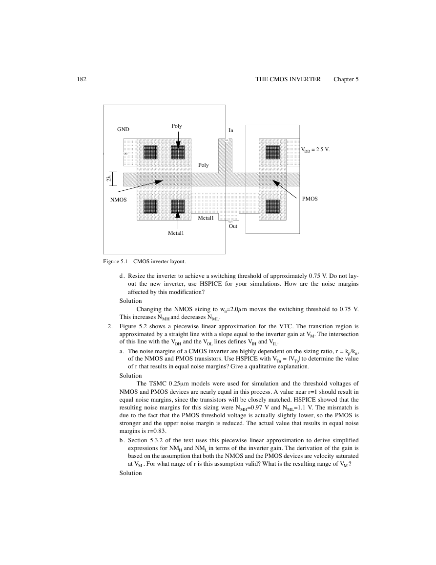
[M, SPICE, 3.3.2] The layout of a static CMOS inverter is given in Figure 5.1. (λ = 0.125
µm).
a. Determine the sizes of the NMOS and PMOS transistors.
Solution
The sizes are wn=1.0µm, ln=0.25µm, wp=0.5µm, and lp=0.25 µm.
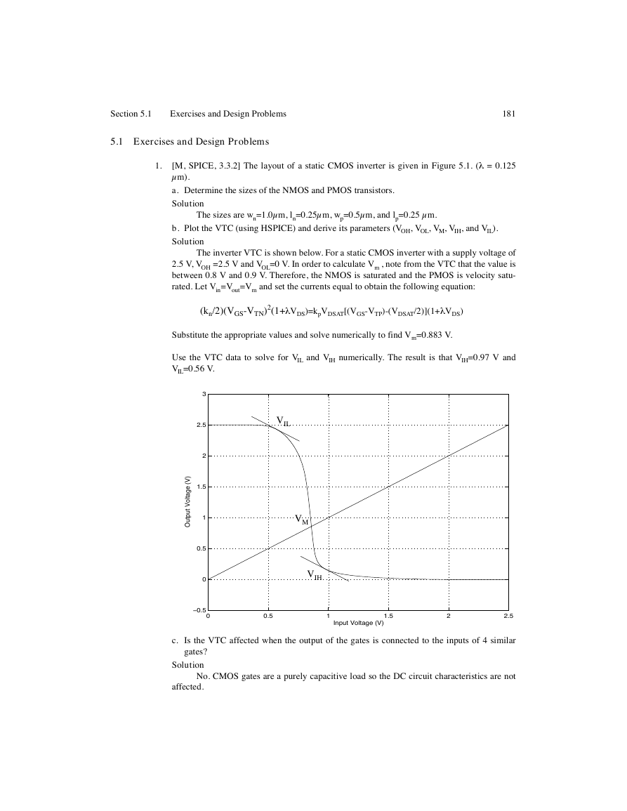
b. Plot the VTC (using HSPICE) and derive its parameters (VOH, VOL, VM, VIH, and VIL).
Solution
The inverter VTC is shown below. For a static CMOS inverter with a supply voltage of
2.5 V, VOH =2.5 V and VOL=0 V. In order to calculate Vm , note from the VTC that the value is
between 0.8 V and 0.9 V. Therefore, the NMOS is saturated and the PMOS is velocity satu-
rated. Let Vin=Vout=Vm and set the currents equal to obtain the following equation:
(kn/2)(VGS-VTN)2(1+λVDS)=kpVDSAT[(VGS-VTP)-(VDSAT/2)](1+λVDS)
Substitute the appropriate values and solve numerically to find Vm=0.883 V.
Use the VTC data to solve for VIL and VIH numerically. The result is that VIH=0.97 V and
VIL=0.56 V.
)
V
(
e
g
a
t
l
o
V
t
u
p
t
u
O
3
2.5
2
1.5
1
0.5
0
−0.5
0
VIL
VM
VIH
0.5
1
1.5
2
2.5
Input Voltage (V)
c.
Is the VTC affected when the output of the gates is connected to the inputs of 4 similar
gates?
Solution
No. CMOS gates are a purely capacitive load so the DC circuit characteristics are not
affected.
�
182
THE CMOS INVERTER
Chapter 5
GND
Poly
In
λ
2
NMOS
Poly
Metal1
Out
Metal1
VDD = 2.5 V.
PMOS
Figure 5.1 CMOS inverter layout.
d. Resize the inverter to achieve a switching threshold of approximately 0.75 V. Do not lay-
out the new inverter, use HSPICE for your simulations. How are the noise margins
affected by this modification?
Solution
Changing the NMOS sizing to wn=2.0µm moves the switching threshold to 0.75 V.
This increases NMH and decreases NML.
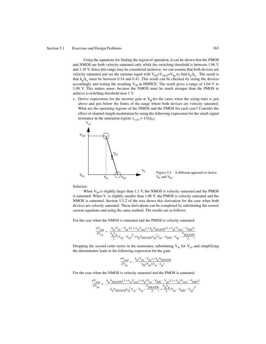
2. Figure 5.2 shows a piecewise linear approximation for the VTC. The transition region is
approximated by a straight line with a slope equal to the inverter gain at VM. The intersection
of this line with the VOH and the VOL lines defines VIH and VIL.
a. The noise margins of a CMOS inverter are highly dependent on the sizing ratio, r = kp/kn,
of the NMOS and PMOS transistors. Use HSPICE with VTn = |VTp| to determine the value
of r that results in equal noise margins? Give a qualitative explanation.
Solution
The TSMC 0.25µm models were used for simulation and the threshold voltages of
NMOS and PMOS devices are nearly equal in this process. A value near r=1 should result in
equal noise margins, since the transistors will be closely matched. HSPICE showed that the
resulting noise margins for this sizing were NMH=0.97 V and NML=1.1 V. The mismatch is
due to the fact that the PMOS threshold voltage is actually slightly lower, so the PMOS is
stronger and the upper noise margin is reduced. The actual value that results in equal noise
margins is r=0.83.
b. Section 5.3.2 of the text uses this piecewise linear approximation to derive simplified
expressions for NMH and NML in terms of the inverter gain. The derivation of the gain is
based on the assumption that both the NMOS and the PMOS devices are velocity saturated
at VM . For what range of r is this assumption valid? What is the resulting range of VM ?
Solution
�
Section 5.1
Exercises and Design Problems
183
Using the equations for finding the region of operation, it can be shown that the PMOS
and NMOS are both velocity saturated only while the switching threshold is between 1.06 V
and 1.10 V. Since this range may be considered inclusive, we can assume that both devices are
velocity saturated and set the currents equal with VIN=VOUT=VM to find kp/kn . The result is
that kp/kn must be between 0.34 and 0.41. This result can be checked by sizing the devices
accordingly and testing the resulting VM in HSPICE. The result gives a range of 1.04 V to
1.09 V. This makes sense, because the NMOS must be much stronger than the PMOS to
achieve a switching threshold near 1 V.
c. Derive expressions for the inverter gain at VM for the cases when the sizing ratio is just
above and just below the limits of the range where both devices are velocity saturated.
What are the operating regions of the NMOS and the PMOS for each case? Consider the
effect of channel-length modulation by using the following expression for the small-signal
resistance in the saturation region: ro,sat = 1/(λID).
Vout
VOH
VOL
Solution:
VM
VIL
VIH
Vin
Figure 5.2 A different approach to derive
VIL and VIH.
When VM is slightly larger than 1.1 V, the NMOS is velocity saturated and the PMOS
is saturated. When V‘ is slightly smaller than 1.06 V, the PMOS is velocity saturated and the
NMOS is saturated. Section 5.3.2 of the text shows this derivation for the case when both
devices are velocity saturated. These derivations can be completed by substituting the correct
current equations and using the same method. The results are as follows:
For the case when the NMOS is saturated and the PMOS is velocity saturated:
dVout
---------------
dVin
–=
–
) 1 λ
+(
(
(
)
–
kn Vin Vtn
p Vout VDD
------------------------------------------------------------------------------------------------------------------------------------------------------------------------
λ
VDSATP
kn
-----------------------
------------ Vin Vtn
2
+(
kpVDSATP 1 λ
λ
p Vin VDD
kpVDSATP
nVout
Vtp
)2
+
+
–
–
–
2
–
n
)
)
(
Dropping the second order terms in the numerator, substituting Vm for Vin, and simplifying
the denominator leads to the following expression for the gain:
dVout
---------------
dVin
–=
kn Vm Vtn
kpVDSATP
-----------------------------------------------------------------------
λ
p–
ID Vm
n
–
(
)
(
)
+
) λ
(
For the case when the NMOS is velocity saturated and the PMOS is saturated:
dVout
---------------
dVin
–=
)
)
)
+(
knVDSATN 1 λ
---------------------------------------------------------------------------------------------------------------------------------------------------------------------------------------
λ
(
p Vout VDD
)2
kp Vin VDD
VDSATN
------------------------
–
Vtp
λ
kp
p
------------ Vin VDD
2
nVout
n Vin Vtn
knVDSATN
) 1 λ
+(
Vtp
+
+
–
–
–
2
–
–
–
(
(
�
184
THE CMOS INVERTER
Chapter 5
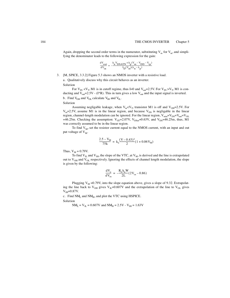
Again, dropping the second order terms in the numerator, substituting Vm for Vin, and simpli-
fying the denominator leads to the following expression for the gain:
dVout
---------------
dVin
–=
)
knVDSATN kp Vm VDD
Vtp
------------------------------------------------------------------------------------------
+
–
–
λ
p–
)
(
) λ
(
n
(
ID Vm
3.
[M, SPICE, 3.3.2] Figure 5.3 shows an NMOS inverter with a resistive load.
a. Qualitatively discuss why this circuit behaves as an inverter.
Solution
For VIN
VT, M1 is con-
ducting and Vout=2.5V - (I*R). This in turn gives a low Vout and the input signal is inverted.
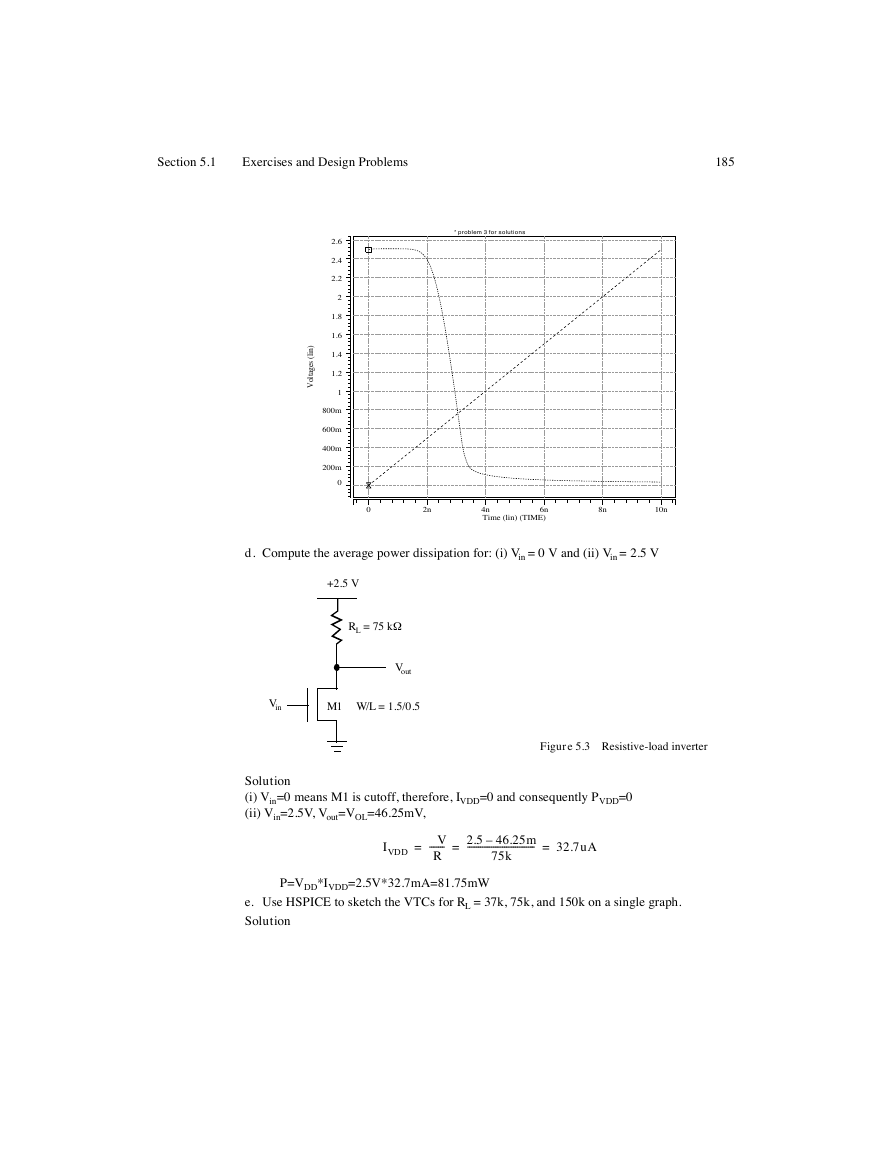
b. Find VOH and VOL calculate VIH and VIL.
Solution
Assuming negligable leakage, when VinSection 5.1
Exercises and Design Problems
185
* problem 3 for solutions
2.6
2.4
2.2
2
1.8
1.6
1.4
1.2
1
800m
600m
400m
200m
0
)
n
i
l
(
s
e
g
a
t
l
o
V
0
2n
4n
6n
Time (lin) (TIME)
8n
10n
d. Compute the average power dissipation for: (i) Vin = 0 V and (ii) Vin = 2.5 V
+2.5 V
RL = 75 kΩ
Vout
Vin
M1 W/L = 1.5/0.5
Figure 5.3 Resistive-load inverter
Solution
(i) Vin=0 means M1 is cutoff, therefore, IVDD=0 and consequently PVDD=0
(ii) Vin=2.5V, Vout=VOL=46.25mV,
IVDD
=
∆V
-------
R
=
2.5
–
46.25m
-------------------------------
75k
=
32.7uA
P=VDD*IVDD=2.5V*32.7mA=81.75mW
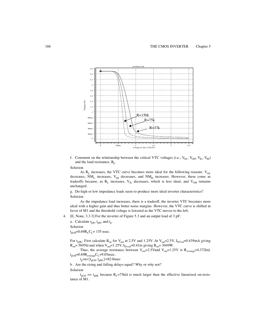
e. Use HSPICE to sketch the VTCs for RL = 37k, 75k, and 150k on a single graph.
Solution
�
186
THE CMOS INVERTER
Chapter 5
2.6
2.4
2.2
2
1.8
1.6
1.4
1.2
1
800m
600m
400m
200m
0
)
n
i
l
(
s
e
g
a
t
l
o
V
* problem 5.3e
R=150k
R=75k
R=37k
0
500m
1
1.5
Voltage X (lin) (VOLTS)
2
2.5
f. Comment on the relationship between the critical VTC voltages (i.e., VOL, VOH, VIL, VIH)
and the load resistance, RL.
Solution
As RL increases, the VTC curve becomes more ideal for the following reasons: VOL
decreases, NML increases, VIH decreases, and NMH increases. However, these come as
tradeoffs because, as RL increases, VIL decreases, which is less ideal, and VOH remains
unchanged.
g. Do high or low impedance loads seem to produce more ideal inverter characteristics?
Solution
As the impedance load increases, there is a tradeoff, the inverter VTC becomes more
ideal with a higher gain and thus better noise margins. However, the VTC curve is shifted in
favor of M1 and the threshold voltage is lowered as the VTC moves to the left.
[E, None, 3.3.3] For the inverter of Figure 5.3 and an output load of 3 pF:
a. Calculate tplh, tphl, and tp.
Solution
tpLH=0.69RLCL= 155 nsec.
4.
For tpHL: First calculate Ron for Vout at 2.5V and 1.25V. At Vout=2.5V, IDVsat=0.439mA giving
Ron= 5695Ω and when Vout=1.25V, IDvsat=0.41m giving Ron= 3049W.
Thus, the average resistance between Vout=2.5Vand Vout=1.25V is Raverage=4.372kΩ.
tpLH=0.69RaverageCL=9.05nsec.
tp=av{tpLH, tpHL}=82.0nsec
b. Are the rising and falling delays equal? Why or why not?
Solution
tpLH >> tpHL because RL=75kΩ is much larger than the effective linearized on-resis-
tance of M1.
�
Section 5.1
Exercises and Design Problems
187
c. Compute the static and dynamic power dissipation assuming the gate is clocked as fast as
possible.
Solution
Static Power:
VIN=VOL gives Vout=VOH=2.5V, thus IVDD=0A so PVDD=0W.
VIN=VOH gives Vout=VOL=46.3mV, which is in the linear region.
Calculating the current through M1 gives IVDD=32.8mA --> PVDD=82mW
Dynamic Power:
Pdyn=CL
∆V*Vdd*fmax=3pF*(2.5V-46.3mV)*2.5V*12.2MHz=0.225mW.
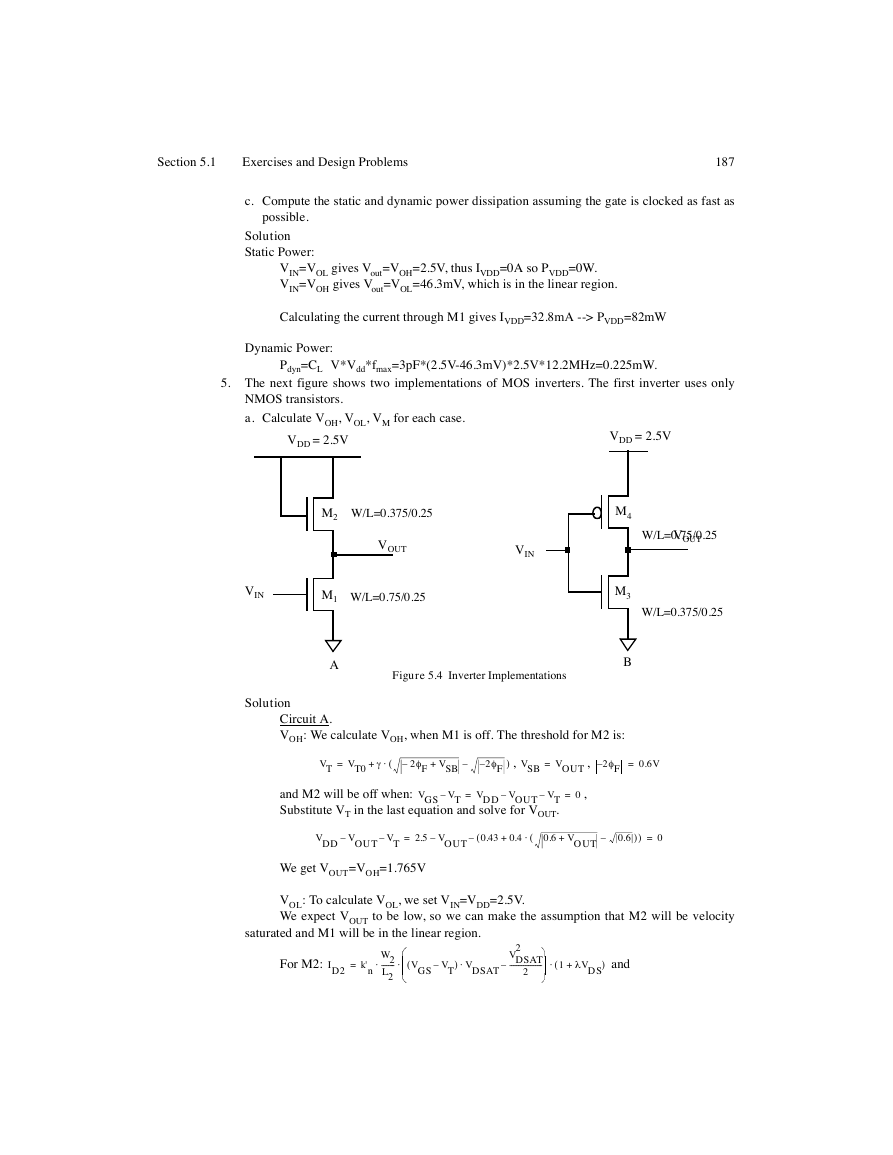
5. The next figure shows two implementations of MOS inverters. The first inverter uses only
NMOS transistors.
a. Calculate VOH, VOL, VM for each case.
VDD = 2.5V
M2
W/L=0.375/0.25
VOUT
VIN
VIN
M1
W/L=0.75/0.25
A
Figure 5.4 Inverter Implementations
VDD = 2.5V
W/L=0.75/0.25
VOUT
W/L=0.375/0.25
M4
M3
B
Solution
Circuit A.
VOH: We calculate VOH, when M1 is off. The threshold for M2 is:
VT
=
VT0
γ
⋅+
(
2φ
–
+
VSB
F
–
2φ
F–
)
,
VSB
=
VOUT
,
2φ
F–
=
0.6V
and M2 will be off when:
VT–
Substitute VT in the last equation and solve for VOUT.
VDD VOUT
–
VGS VT–
=
=
0
,
VDD VOUT
–
VT–
=
–
2.5 VOUT
–
(
0.43
+
0.4
⋅
(
+
0.6 VOUT
–
)
)
0.6
=
0
We get VOUT=VOH=1.765V
VOL: To calculate VOL, we set VIN=VDD=2.5V.
We expect VOUT to be low, so we can make the assumption that M2 will be velocity
saturated and M1 will be in the linear region.
For M2:
ID2
=
k'n
⋅
⋅
W2
--------
L2
(
VGS VT–
⋅
) VDSAT
–
2
VDSAT
-------------------
2
⋅
1 λVDS
+(
)
and
�


 2023年江西萍乡中考道德与法治真题及答案.doc
 2012年重庆南川中考生物真题及答案.doc
 2013年江西师范大学地理学综合及文艺理论基础考研真题.doc
 2020年四川甘孜小升初语文真题及答案I卷.doc
 2020年注册岩土工程师专业基础考试真题及答案.doc
 2023-2024学年福建省厦门市九年级上学期数学月考试题及答案.doc
 2021-2022学年辽宁省沈阳市大东区九年级上学期语文期末试题及答案.doc
 2022-2023学年北京东城区初三第一学期物理期末试卷及答案.doc
 2018上半年江西教师资格初中地理学科知识与教学能力真题及答案.doc
 2012年河北国家公务员申论考试真题及答案-省级.doc
 2020-2021学年江苏省扬州市江都区邵樊片九年级上学期数学第一次质量检测试题及答案.doc
 2022下半年黑龙江教师资格证中学综合素质真题及答案.doc