PX30 Datasheet Rev 1.0
Rockchip
PX30
Datasheet
Revision 1.0
April. 2018
Copyright 2018 ©Fuzhou Rockchip Electronics Co., Ltd. - 1 -
�
PX30 Datasheet Rev 1.0
Date
Revision
Revision History
Description
2018-4-2
1.0
Initial released
Copyright 2018 ©Fuzhou Rockchip Electronics Co., Ltd. - 2 -
�
PX30 Datasheet Rev 1.0
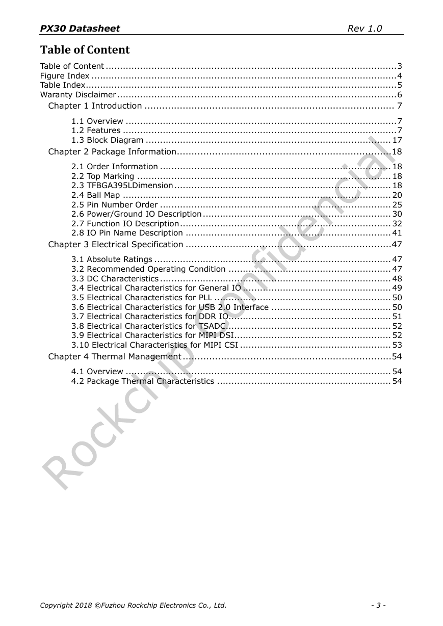
Table of Content
Table of Content ...................................................................................................... 3
Figure Index ........................................................................................................... 4
Table Index ............................................................................................................. 5
Waranty Disclaimer .................................................................................................. 6
Chapter 1 Introduction ..................................................................................... 7
1.1 Overview ............................................................................................... 7
1.2 Features ................................................................................................ 7
1.3 Block Diagram ...................................................................................... 17
Chapter 2 Package Information......................................................................... 18
2.1 Order Information ................................................................................. 18
2.2 Top Marking ......................................................................................... 18
2.3 TFBGA395LDimension ............................................................................ 18
2.4 Ball Map .............................................................................................. 20
2.5 Pin Number Order ................................................................................. 25
2.6 Power/Ground IO Description .................................................................. 30
2.7 Function IO Description .......................................................................... 32
2.8 IO Pin Name Description ........................................................................ 41
Chapter 3 Electrical Specification ...................................................................... 47
3.1 Absolute Ratings ................................................................................... 47
3.2 Recommended Operating Condition ......................................................... 47
3.3 DC Characteristics ................................................................................. 48
3.4 Electrical Characteristics for General IO .................................................... 49
3.5 Electrical Characteristics for PLL .............................................................. 50
3.6 Electrical Characteristics for USB 2.0 Interface .......................................... 50
3.7 Electrical Characteristics for DDR IO......................................................... 51
3.8 Electrical Characteristics for TSADC.......................................................... 52
3.9 Electrical Characteristics for MIPI DSI ....................................................... 52
3.10 Electrical Characteristics for MIPI CSI ..................................................... 53
Chapter 4 Thermal Management ....................................................................... 54
4.1 Overview ............................................................................................. 54
4.2 Package Thermal Characteristics ............................................................. 54
Copyright 2018 ©Fuzhou Rockchip Electronics Co., Ltd. - 3 -
�
PX30 Datasheet Rev 1.0
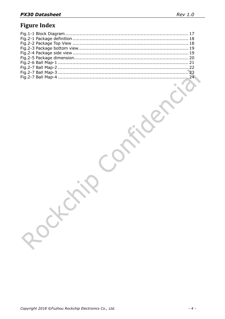
Figure Index
Fig.1-1 Block Diagram ..................................................................................... 17
Fig.2-1 Package definition ................................................................................ 18
Fig.2-2 Package Top View ................................................................................ 18
Fig.2-3 Package bottom view ............................................................................ 19
Fig.2-4 Package side view ................................................................................ 19
Fig.2-5 Package dimension ............................................................................... 20
Fig.2-6 Ball Map-1 .......................................................................................... 21
Fig.2-7 Ball Map-2 .......................................................................................... 22
Fig.2-7 Ball Map-3 .......................................................................................... 23
Fig.2-7 Ball Map-4 .......................................................................................... 24
Copyright 2018 ©Fuzhou Rockchip Electronics Co., Ltd. - 4 -
�
PX30 Datasheet Rev 1.0
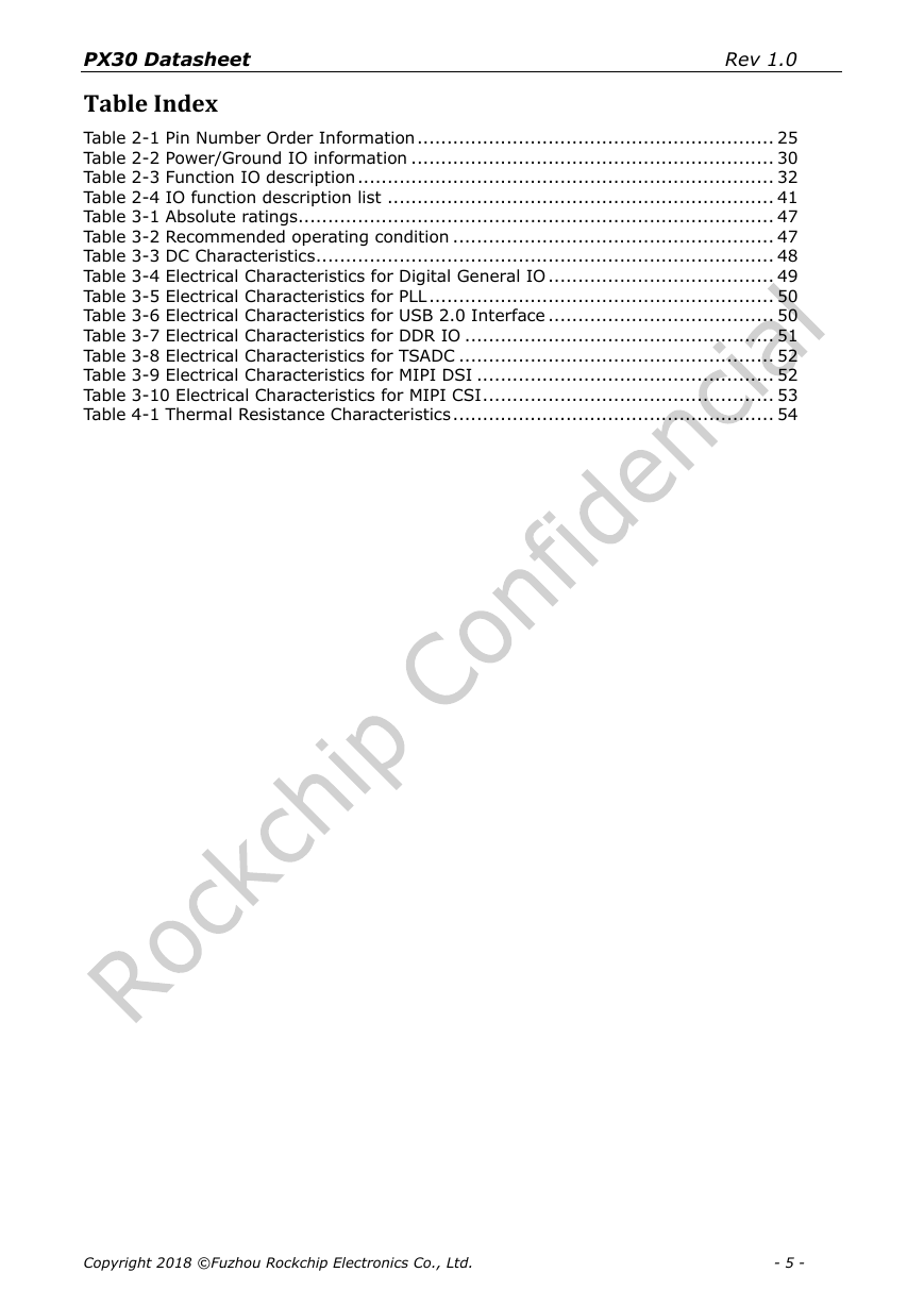
Table Index
Table 2-1 Pin Number Order Information ............................................................ 25
Table 2-2 Power/Ground IO information ............................................................. 30
Table 2-3 Function IO description ...................................................................... 32
Table 2-4 IO function description list ................................................................. 41
Table 3-1 Absolute ratings................................................................................ 47
Table 3-2 Recommended operating condition ...................................................... 47
Table 3-3 DC Characteristics ............................................................................. 48
Table 3-4 Electrical Characteristics for Digital General IO ...................................... 49
Table 3-5 Electrical Characteristics for PLL .......................................................... 50
Table 3-6 Electrical Characteristics for USB 2.0 Interface ...................................... 50
Table 3-7 Electrical Characteristics for DDR IO .................................................... 51
Table 3-8 Electrical Characteristics for TSADC ..................................................... 52
Table 3-9 Electrical Characteristics for MIPI DSI .................................................. 52
Table 3-10 Electrical Characteristics for MIPI CSI ................................................. 53
Table 4-1 Thermal Resistance Characteristics ...................................................... 54
Copyright 2018 ©Fuzhou Rockchip Electronics Co., Ltd. - 5 -
�
PX30 Datasheet Rev 1.0
Waranty Disclaimer
Rockchip Electronics Co., Ltd makes no warranty, representation or guarantee (expressed, implied, statutory, or otherwise) by
or with respect to anything in this document, and shall not be liable for any implied warranties of non-infringement,
merchantability or fitness for a particular purpose or for any indirect, special or consequential damages.
Information furnished is believed to be accurate and reliable. However, Rockchip Electronics Co., Ltd assumes no responsibility
for the consequences of use of such information or for any infringement of patents or other rights of third parties that may result
from its use.
Rockchip Electronics Co., Ltd’s products are not designed, intended, or authorized for using as components in systems intended
for surgical implant into the body, or other applications intended to support or sustain life, or for any other application in which
the failure of the Rockchip Electronics Co., Ltd’s product could create a situation where personal injury or death may occur,
should buyer purchase or use Rockchip Electronics Co., Ltd’s products for any such unintended or unauthorized application,
buyers shall indemnify and hold Rockchip Electronics Co., Ltd and its officers, employees, subsidiaries, affiliates, and distributors
harmless against all claims, costs, damages, expenses, and reasonable attorney fees arising out of, either directly or indirectly,
any claim of personal injury or death that may be associated with such unintended or unauthorized use, even if such claim
alleges that Rockchip Electronics Co., Ltd was negligent regarding the design or manufacture of the part.
Copyright and Patent Right
Information in this document is provided solely to enable system and software implementers to use Rockchip Electronics Co.,
Ltd ’s products. There are no expressed or implied copyright licenses granted hereunder to design or fabricate any integrated
circuits or integrated circuits based on the information in this document.
Rockchip Electronics Co., Ltd does not convey any license under its patent rights nor the rights
of others.
All copyright and patent rights referenced in this document belong to their respective owners
and shall be subject to corresponding copyright and patent licensing requirements.
Trademarks
Rockchip and RockchipTM logo and the name of Rockchip Electronics Co., Ltd’s products are trademarks of Rockchip Electronics
Co., Ltd. and are exclusively owned by Rockchip Electronics Co., Ltd. References to other companies and their products use
trademarks owned by the respective companies and are for reference purpose only.
Confidentiality
The information contained herein (including any attachments) is confidential. The recipient hereby acknowledges the
confidentiality of this document, and except for the specific purpose, this document shall not be disclosed to any third party.
Reverse engineering or disassembly is prohibited.
ROCKCHIP ELECTRONICS CO.,LTD. RESERVES THE RIGHT TO MAKE CHANGES IN ITS PRODUCTS OR PRODUCT
SPECIFICATIONS WITH THE INTENT TO IMPROVE FUNCTION OR DESIGN AT ANY TIME AND WITHOUT NOTICE
AND IS NOT REQUIRED TO UNDATE THIS DOCUMENTATION TO REFLECT SUCH CHANGES.
Copyright © 2018 Rockchip Electronics Co., Ltd.
All rights reserved. No part of this publication may be reproduced, stored in a retrieval system, or transmitted in any form or by
any means, electric or mechanical, by photocopying, recording, or otherwise, without the prior written consent of Rockchip
Electronics Co., Ltd.
Copyright 2018 ©Fuzhou Rockchip Electronics Co., Ltd. - 6 -
�
PX30 Datasheet Rev 1.0
Chapter 1 Introduction
1.1 Overview
PX30 is a high-performance Quad-core application processor designed for personal mobile
internet device and other digital multimedia applications.
Many embedded powerful hardware engines are provided to optimize performance for
high-end application. PX30 supports almost full-format H.264 decoder by 1080p@60fps,
H.265 decoder by 1080p@60fps, also support H.264 encoder by 1080p@30fps, high-quality
JPEG encoder/decoder.
Embedded 3D GPU makes PX30 completely compatible with OpenGL ES 1.1/2.0/3.2, DirectX
11 FL9_3, OpenCL 2.0 and Vulkan 1.0. Special 2D hardware engine will maximize display
performance and provide very smoothly operation.
PX30 has high-performance external memory interface
(DDR3/DDR3L/DDR4/LPDDR2/LPDDR3) capable of sustaining demanding memory
bandwidths.
1.2 Features
The features listed below which may or may not be present in actual product, may be subject
to the third party licensing requirements. Please contact Rockchip for actual product feature
configurations and licensing requirements.
1.2.1 Microprocessor
Quad-core ARM Cortex-A35 CPU
Full implementation of the ARM architecture v8-A instruction set
ARM Neon Advanced SIMD (single instruction, multiple data) support for accelerated
media and signal processing computation
In-order pipeline with symmetric dual-issue of most instructions
ARMv8 Cryptography Extensions
256KB unified system L2 cache
TrustZone technology support
Separate power domains for CPU core system to support internal power switch and
Include VFP v3 hardware to support single and double-precision operations
Integrated 32KB L1 instruction cache, 32KB L1 data cache with 4-way set associative
externally turn on/off based on different application scenario
PD_A35_0: 1st Cortex-A35 + Neon + FPU + L1 I/D Cache
PD_A35_1: 2nd Cortex-A35 + Neon + FPU + L1 I/D Cache
PD_A35_2: 3rd Cortex-A35 + Neon + FPU + L1 I/D Cache
PD_A35_3: 4th Cortex-A35 + Neon + FPU + L1 I/D Cache
One isolated voltage domain to support DVFS
1.2.2 Memory Organization
Internal on-chip memory
BootROM
SYSTEM_SRAM in the voltage domain of VD_LOGIC
PMU_SRAM in the voltage domain of VD_PMU for low power application
External off-chip memory①
DDR3/DDR3L/DDR4/LPDDR2/LPDDR3
SPI Flash
eMMC
SD_Card
Copyright 2018 ©Fuzhou Rockchip Electronics Co., Ltd. - 7 -
�
PX30 Datasheet Rev 1.0
8bits Async Nand Flash
8bits toggle Nand Flash
8bit ONFI Nand Flash
1.2.3 Internal Memory
Internal BootRom
Support system boot from the following device:
SPI Flash interface
eMMC interface
SDMMC interface
Toggle Nand Flash
Async Nand FLash
Support system code download by the following interface:
USB OTG interface (Device mode)
SYSTEM_SRAM
Size: 16KB
PMU_SRAM
Size: 8KB
1.2.4 External Memory or Storage device
Dynamic Memory Interface (DDR3/DDR3L/DDR4/LPDDR2/LPDDR3)
Compatible with JEDEC standards
Compatible with DDR3-1600/DDR3L-1600/DDR4-1600/LPDDR2-1066
/LPDDR3-1600
Support 32-bit data width, 2 ranks (chip selects), max 4GB addressing space per rank;
total addressing space is 4GB(max) also
Low power modes, such as power-down and self-refresh for SDRAM
Compensation for board delays and variable latencies through programmable
pipelines
Programmable output and ODT impedance with dynamic PVT compensation
eMMC Interface
Compatible with standard iNAND interface
Compatible with eMMC specification 4.41, 4.51, 5.0 and 5.1
Support three data bus width: 1-bit, 4-bit or 8-bit
Support up to HS200; but not support CMD Queue
SD/MMC Interface
Compatible with SD3.0, MMC ver4.51
Data bus width is 4bits
Nand Flash Interface
Support async nand flash, each channel 8bits, up to 4 banks
Support ONFI Synchronous Flash Interface, each channel 8bits, up to 4 banks
Support Toggle Flash Interface, each channel 8bits, up to 4 banks
Support LBA nand flash in async or sync mode
Up to 70bits/1KB hardware ECC
For DDR nand flash, support DLL bypass and 1/4 or 1/8 clock adjust, maximum clock
rate is 75MHz
For async nand flash, support configurable interface timing , maximum data rate is
8bit/cycle
1.2.5 System Component
CRU (clock & reset unit)
Copyright 2018 ©Fuzhou Rockchip Electronics Co., Ltd. - 8 -
�



 2023年江西萍乡中考道德与法治真题及答案.doc
 2012年重庆南川中考生物真题及答案.doc
 2013年江西师范大学地理学综合及文艺理论基础考研真题.doc
 2020年四川甘孜小升初语文真题及答案I卷.doc
 2020年注册岩土工程师专业基础考试真题及答案.doc
 2023-2024学年福建省厦门市九年级上学期数学月考试题及答案.doc
 2021-2022学年辽宁省沈阳市大东区九年级上学期语文期末试题及答案.doc
 2022-2023学年北京东城区初三第一学期物理期末试卷及答案.doc
 2018上半年江西教师资格初中地理学科知识与教学能力真题及答案.doc
 2012年河北国家公务员申论考试真题及答案-省级.doc
 2020-2021学年江苏省扬州市江都区邵樊片九年级上学期数学第一次质量检测试题及答案.doc
 2022下半年黑龙江教师资格证中学综合素质真题及答案.doc