ADC0831A, ADC0832A, ADC0831B, ADC0832B
A/D PERIPHERALS WITH SERIAL CONTROL
SLAS006 – AUGUST 1985 – REVISED JUNE 1986
D 8-Bit Resolution
D Easy Microprocessor interface or
Stand-Alone Operation
D Operates Ratiometrically or With 5-V
Reference
D Single Channel or Multiplexed Twin
Channels With Single-Ended or Differential
Input Options
D Input Range 0 to 5 V With Single 5-V Supply
D Inputs and Outputs Are Compatible With
TTL and MOS
D Conversion Time of 32 m s at CLK = 250 kHz
D Designed to Be interchangeable With
National Semiconductor ADC0831 and
ADC0832
DEVICE
DEVICE
ADC0831
ADC0832
TOTAL UNADJUSTED ERROR
A-SUFFIX
± 1 LSB
± 1 LSB
B-SUFFIX
± 1/2 LSB
± 1/2 LSB
description
ADC0831 . . . P PACKAGE
(TOP VIEW)
CS
IN+
IN–
GND
1
2
3
4
8
7
6
5
VCC
CLK
DO
REF
ADC0832 . . . P PACKAGE
(TOP VIEW)
CS
CH0
CH1
GND
1
2
3
4
8
7
6
5
VCC/REF
CLK
DO
DI
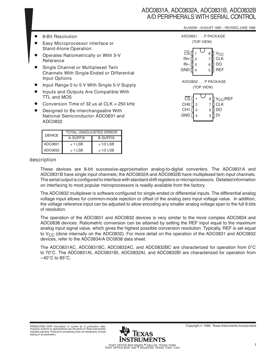
These devices are 8-bit successive-approximation analog-to-digital converters. The ADC0831A and
ADC0831B have single input channels; the ADC0832A and ADC0832B have multiplexed twin input channels.
The serial output is configured to interface with standard shift registers or microprocessors. Detailed information
on interfacing to most popular microprocessors is readily available from the factory.
The ADC0832 multiplexer is software configured for single-ended or differential inputs. The differential analog
voltage input allows for common-mode rejection or offset of the analog zero input voltage value. In addition,
the voltage reference input can be adjusted to allow encoding any smaller analog voltage span to the full 8 bits
of resolution.
The operation of the ADC0831 and ADC0832 devices is very similar to the more complex ADC0834 and
ADC0838 devices. Ratiometric conversion can be attained by setting the REF input equal to the maximum
analog input signal value, which gives the highest possible conversion resolution. Typically, REF is set equalto V
CC (done internally on the ADC0832). For more detail on the operation of the ADC0831 and ADC0832
devices, refer to the ADC0834/A DC0838 data sheet.
The ADC0831AC, ADC0831BC, ADC0832AC, and ADC0832BC are characterized for operation from 0°C
to 70°C. The ADC0831AI, ADC0831BI, ADC0832AI, and ADC0832BI are characterized for operation from
–40°C to 85°C.
PRODUCTION DATA information is current as of publication date.
Products conform to specifications per the terms of Texas Instruments
standard warranty. Production processing does not necessarily include
testing of all parameters.
Copyright 1996, Texas Instruments Incorporated
POST OFFICE BOX 655303 • DALLAS, TEXAS 75265
POST OFFICE BOX 1443 • HOUSTON, TEXAS 77251–1443
1
�
ADC0831A, ADC0832A, ADC0831B, ADC0832B
A/D PERIPHERALS WITH SERIAL CONTROL
SLAS006 – AUGUST 1985 – REVISED JUNE 1986
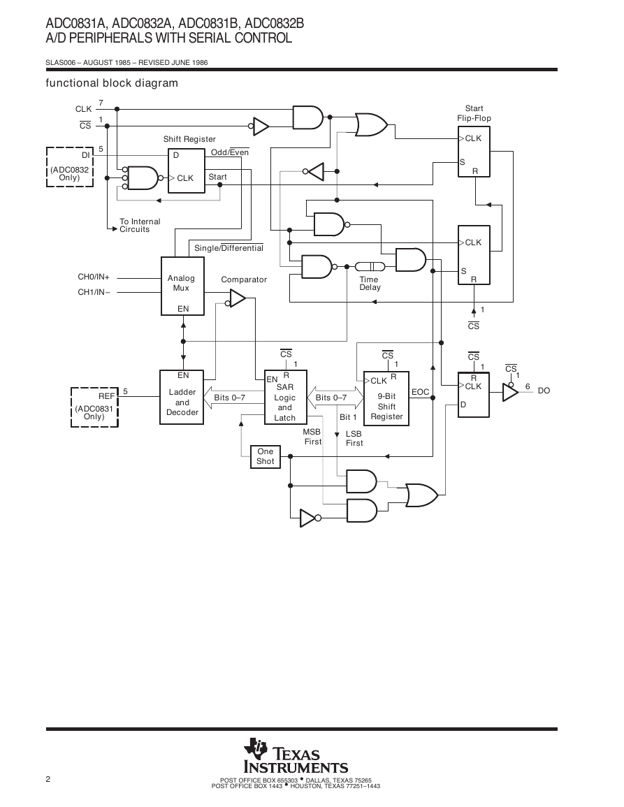
functional block diagram
7
1
5
CLK
CS
DI
(ADC0832
Only)
Shift Register
D
Odd/Even
CLK
Start
To Internal
Circuits
Single/Differential
CH0/IN+
CH1/IN –
Analog
Mux
EN
Comparator
Time
Delay
5
REF
(ADC0831
Only)
EN
Ladder
and
Decoder
Bits 0–7
CS
1
REN
SAR
Logic
and
Latch
One
Shot
CS
1
R
CLK
Bits 0–7
EOC
9-Bit
Shift
Bit 1
Register
MSB
First
LSB
First
Start
Flip-Flop
CLK
S
R
CLK
S
R
1
CS
CS
1
R
CLK
D
CS
1
6
DO
2
POST OFFICE BOX 655303 • DALLAS, TEXAS 75265
POST OFFICE BOX 1443 • HOUSTON, TEXAS 77251–1443
�
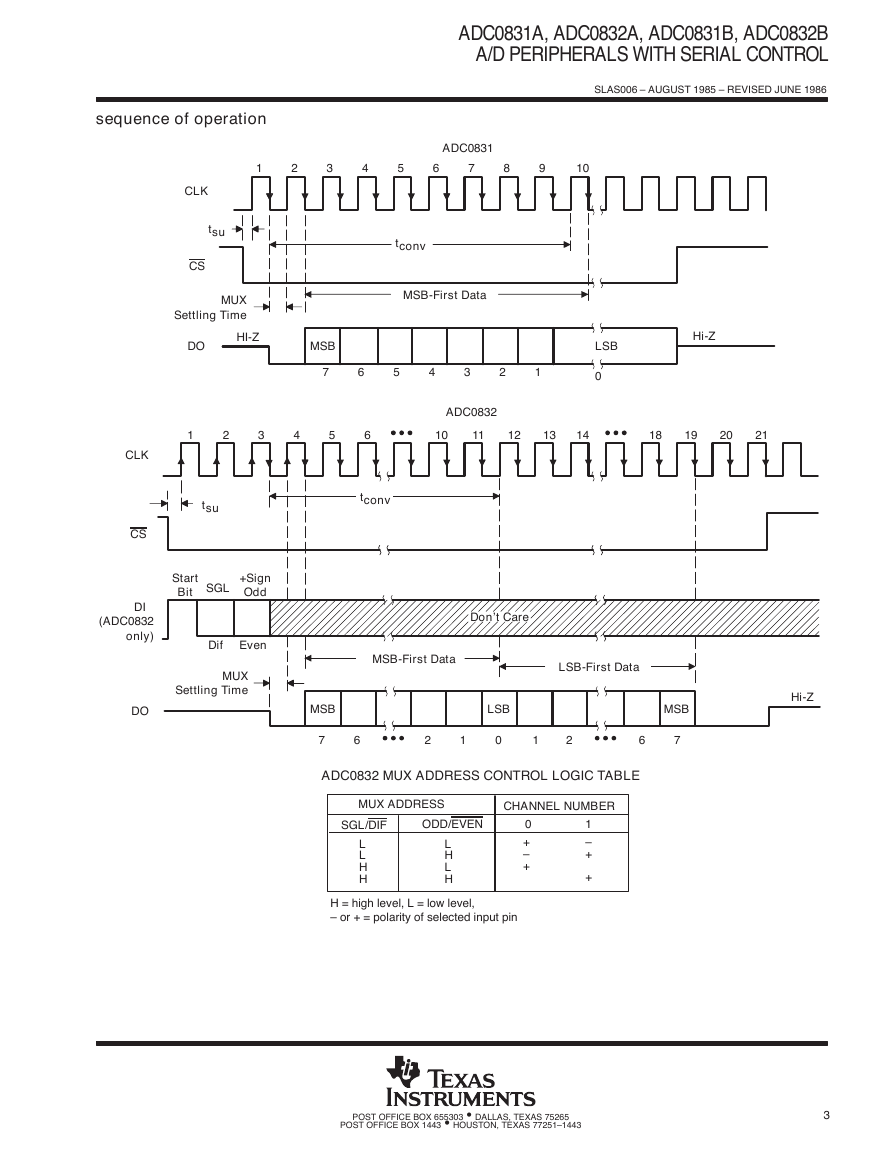
sequence of operation
ADC0831A, ADC0832A, ADC0831B, ADC0832B
A/D PERIPHERALS WITH SERIAL CONTROL
SLAS006 – AUGUST 1985 – REVISED JUNE 1986
1
2
3
4
5
6
7
8
9
10
ADC0831
CLK
tsu
CS
MUX
Settling Time
HI-Z
DO
MSB
tconv
MSB-First Data
7
6
5
4
3
2
1
ADC0832
Hi-Z
LSB
0
1
2
3
4
5
6
10
11
12
13
14
18
19
20
21
CLK
CS
DI
(ADC0832
only)
tsu
tconv
Start
Bit
SGL
+Sign
Odd
Dif
Even
MUX
Settling Time
Don’t Care
MSB-First Data
LSB-First Data
DO
MSB
LSB
MSB
Hi-Z
7
6
2
1
0
1
2
6
7
ADC0832 MUX ADDRESS CONTROL LOGIC TABLE
MUX ADDRESS
CHANNEL NUMBER
SGL/DIF
ODD/EVEN
L
L
H
H
L
H
L
H
0
+
–
+
1
–
+
+
H = high level, L = low level,
– or + = polarity of selected input pin
POST OFFICE BOX 655303 • DALLAS, TEXAS 75265
POST OFFICE BOX 1443 • HOUSTON, TEXAS 77251–1443
3
�
ADC0831A, ADC0832A, ADC0831B, ADC0832B
A/D PERIPHERALS WITH SERIAL CONTROL
SLAS006 – AUGUST 1985 – REVISED JUNE 1986
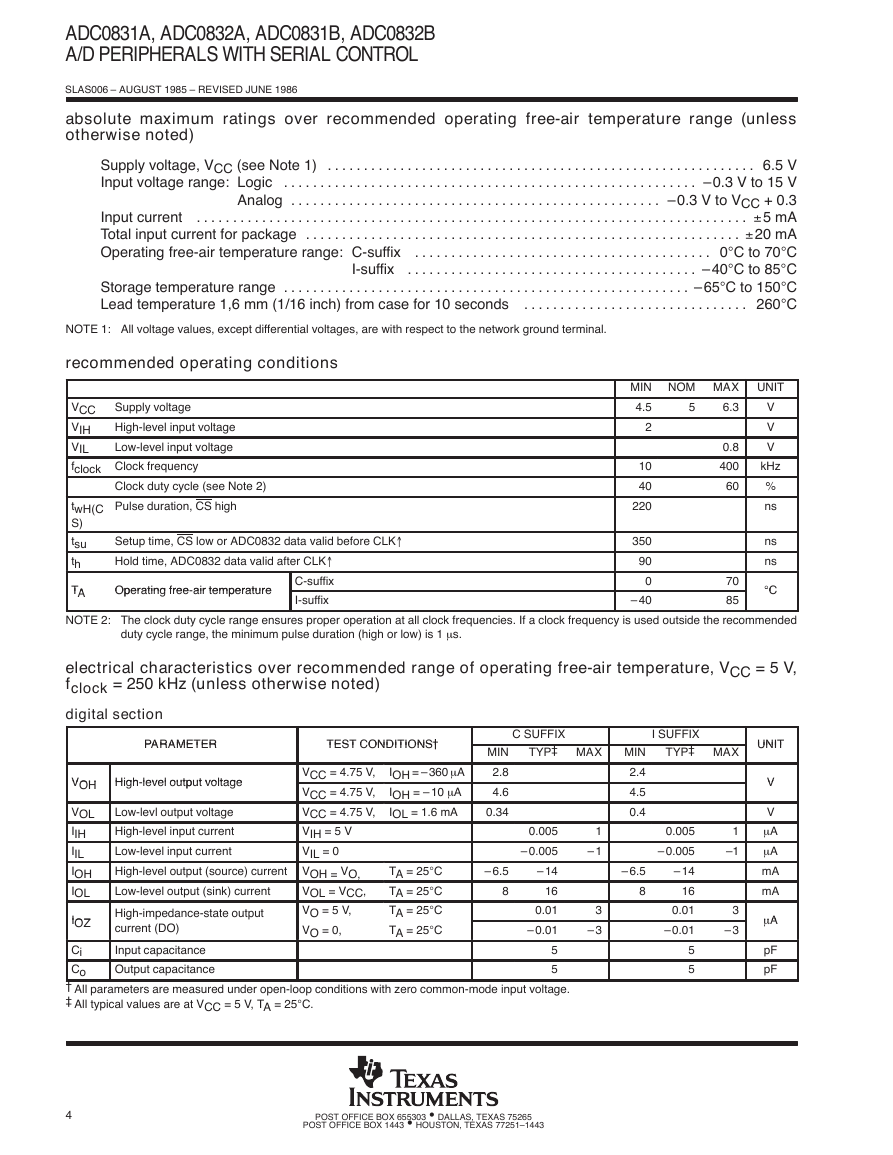
absolute maximum ratings over recommended operating free-air temperature range (unless
otherwise noted)
Supply voltage, VCC (see Note 1)
Input voltage range: Logic
. . . . . . . . . . . . . . . . . . . . . . . . . . . . . . . . . . . . . . . . . . . . . . . . . . . . . . . . . . .
. . . . . . . . . . . . . . . . . . . . . . . . . . . . . . . . . . . . . . . . . . . . . . . . . . . . . . . . .
. . . . . . . . . . . . . . . . . . . . . . . . . . . . . . . . . . . . . . . . . . . . . . . . . . .
Analog
. . . . . . . . . . . . . . . . . . . . . . . . . . . . . . . . . . . . . . . . . . . . . . . . . . . . . . . . . . . . . . . . . . . . . . . . . . . .
. . . . . . . . . . . . . . . . . . . . . . . . . . . . . . . . . . . . . . . . . . . . . . . . . . . . . . . . . . . .
Input current
Total input current for package
Operating free-air temperature range: C-suffix
I-suffix
Storage temperature range
Lead temperature 1,6 mm (1/16 inch) from case for 10 seconds
. . . . . . . . . . . . . . . . . . . . . . . . . . . . . . .
. . . . . . . . . . . . . . . . . . . . . . . . . . . . . . . . . . . . . . . . .
. . . . . . . . . . . . . . . . . . . . . . . . . . . . . . . . . . . . . . . .
. . . . . . . . . . . . . . . . . . . . . . . . . . . . . . . . . . . . . . . . . . . . . . . . . . . . . . . .
6.5 V
–0.3 V to 15 V
–0.3 V to VCC + 0.3
±5 mA
±20 mA
0°C to 70°C
–40°C to 85°C
–65°C to 150°C
260°C
NOTE 1: All voltage values, except differential voltages, are with respect to the network ground terminal.
recommended operating conditions
Supply voltage
High-level input voltage
Low-level input voltage
VCC
VIH
VIL
fclock Clock frequency
twH(C
S)
tsu
th
TA
TA
Clock duty cycle (see Note 2)
Pulse duration, CS high
Setup time, CS low or ADC0832 data valid before CLK↑
Hold time, ADC0832 data valid after CLK↑
C-suffix
I-suffix
Operating free air temperature
Operating free-air temperature
MIN NOM MAX
4.5
6.3
2
5
10
40
220
350
90
0
– 40
0.8
400
60
70
85
UNIT
V
V
V
kHz
%
ns
ns
ns
°C
°C
NOTE 2: The clock duty cycle range ensures proper operation at all clock frequencies. If a clock frequency is used outside the recommended
duty cycle range, the minimum pulse duration (high or low) is 1 m s.
electrical characteristics over recommended range of operating free-air temperature, VCC = 5 V,
fclock = 250 kHz (unless otherwise noted)
digital section
PARAMETER
PARAMETER
TEST CONDITIONS{
TEST CONDITIONS{
VOH
VOH
VOL
IIH
IIL
IOH
IOL
IOZ
IOZ
High level output voltage
High-level output voltage
VCC = 4.75 V,
VCC = 4.75 V,
VCC = 4.75 V,
VIH = 5 V
VIL = 0
Low-levl output voltage
High-level input current
Low-level input current
High-level output (source) current VOH = VO,
VOL = VCC,
Low-level output (sink) current
VO = 5 V,
VO = 0,
High-impedance-state output
current (DO)
g
IOH = – 360 m A
IOH = – 10 m A
IOL = 1.6 mA
TA = 25°C
TA = 25°C
TA = 25°C
TA = 25°C
MIN
2.8
4.6
0.34
– 6.5
8
Input capacitance
Output capacitance
Ci
Co
† All parameters are measured under open-loop conditions with zero common-mode input voltage.
‡ All typical values are at VCC = 5 V, TA = 25°C.
C SUFFIX
TYP‡ MAX
1
– 1
3
– 3
0.005
– 0.005
– 14
16
0.01
– 0.01
5
5
MIN
2.4
4.5
0.4
– 6.5
8
I SUFFIX
TYP‡ MAX
UNIT
UNIT
V
V
V
m A
m A
mA
mA
m A
m A
pF
pF
1
–1
3
– 3
0.005
– 0.005
– 14
16
0.01
– 0.01
5
5
4
POST OFFICE BOX 655303 • DALLAS, TEXAS 75265
POST OFFICE BOX 1443 • HOUSTON, TEXAS 77251–1443
�
ADC0831A, ADC0832A, ADC0831B, ADC0832B
A/D PERIPHERALS WITH SERIAL CONTROL
SLAS006 – AUGUST 1985 – REVISED JUNE 1986
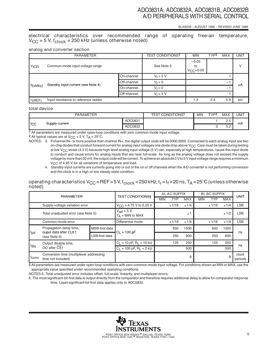
electrical characteristics over recommended range of operating
VCC = 5 V, fclock = 250 kHz (unless otherwise noted)
analog and converter section
free-air
temperature,
PARAMETER
TEST CONDITIONS†
VICR
Common-mode input voltage range
II( tdb ) Standby input current (see Note 4)
II(stdby) Standby input current (see Note 4)
On-channel
Off-channel
On-channel
Off-channel
See Note 3
VI = 5 V
VI = 0
VI = 0
VI = 5 V
MIN
– 0.05
to
VCC+ 0.05
ri(REF)
Input resistance to reference ladder
1.3
2.4
V
m A
m A
kW
1
– 1
– 1
1
5.9
TYP‡ MAX
UNIT
total device
ICC
ICC
Supply current
Supply current
PARAMETER
TEST CONDITIONS†
MIN
ADC0831
ADC0832
TYP‡ MAX
2.5
5.2
1
3
UNIT
mA
mA
† All parameters are measured under open-loop conditions with zero common-mode input voltage.
‡ All typical values are at VCC = 5 V, TA = 25°C.
NOTES: 3.
If channel IN– is more positive than channel IN+, the digital output code will be 0000 0000. Connected to each analog input are two
on-chip diodes that conduct forward current for analog input voltages one diode drop above VCC .Care must be taken during testing
at low VCC levels (4.5 V) because high-level analog input voltage (5 V) can, especially at high temperatures, cause this input diode
to conduct and cause errors for analog inputs that are near full-scale. As long as the analog voltage does not exceed the supply
voltage by more than 50 mV, the output code will be correct. To achieve an absolute 0 V to 5 V input voltage range requires a minimum
VCC of 4.95 V for all variations of temperature and load.
4. Standby input currents are currents going into or out of the on or off channels when the A/D converter is not performing conversion
and the clock is in a high or low steady-state condition.
operating characteristics VCC = REF = 5 V, fclock = 250 kHz, tr = tf = 20 ns, TA = 25°C (unless otherwise
noted)
PARAMETER
PARAMETER
TEST CONDITIONS§
TEST CONDITIONS§
tconv
clock
periods
§ All parameters are measured under open-loop conditions with zero common-mode input voltage. For conditions shown as MIN or MAX, use the
8
8
appropriate value specified under recommended operating conditions.
NOTES:5. Total unadjusted error includes offset, full-scale, linearity, and multiplexer errors.
6. The most significant-bit-first data is output directly from the comparator and therefore requires additional delay to allow for comparator response
time. Least-significant-bit-first data applies only to ADC0832.
POST OFFICE BOX 655303 • DALLAS, TEXAS 75265
POST OFFICE BOX 1443 • HOUSTON, TEXAS 77251–1443
5
Supply-voltage variation error
Total unadjusted error (see Note 5)
Common-mode error
Propagation delay time,
ouput data after CLK↑
ouput data after CLK↑
(see Note 6)
Output disable time,
,
DO after CS↑
Conversion time (multiplexer addressing
time not included)
t d
tpd
tdi
tdis
VCC = 4.75 V to 5.25 V
Vref = 5 V,
TA = MIN to MAX
Differential mode
MSB-first data
LSB-first data
CL = 100 pF
CL = 100 pF
CL = 10 pF, RL = 10 kW
CL = 100 pF, RL = 2 kW
AI, AC SUFFIX
BI, BC SUFFIX
MIN
TYP MAX
± 1/4
± 1/16
MIN
TYP MAX
± 1/4
± 1/16
± 1/16
650
250
125
± 1
± 1/4
1500
600
250
500
± 1/16
650
250
125
± 1/2
± 1/4
1500
600
250
500
UNIT
UNIT
LSB
LSB
LSB
ns
ns
ns
ns
�
ADC0831A, ADC0832A, ADC0831B, ADC0832B
A/D PERIPHERALS WITH SERIAL CONTROL
SLAS006 – AUGUST 1985 – REVISED JUNE 1986
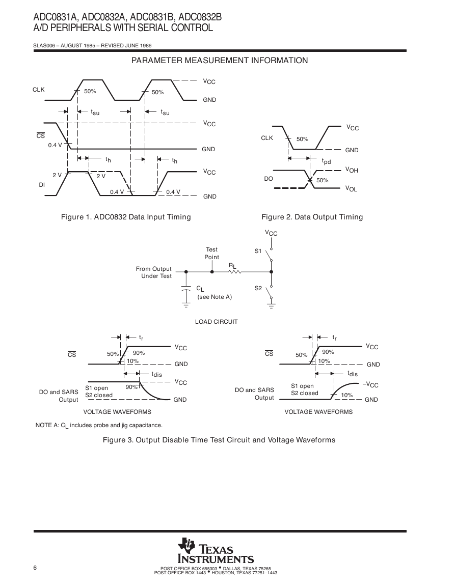
PARAMETER MEASUREMENT INFORMATION
CLK
50%
tsu
CS
0.4 V
2 V
DI
th
2 V
50%
tsu
th
VCC
GND
VCC
GND
VCC
GND
CLK
50%
DO
tpd
50%
VCC
GND
VOH
VOL
0.4 V
0.4 V
Figure 1. ADC0832 Data Input Timing
Figure 2. Data Output Timing
From Output
Under Test
VCC
S1
S2
Test
Point
RL
CL
(see Note A)
LOAD CIRCUIT
tr
CS
50%
90%
10%
DO and SARS
Output
S1 open
S2 closed
90%
tdis
VCC
GND
VCC
GND
CS
50%
tr
90%
10%
DO and SARS
Output
S1 open
S2 closed
VCC
GND
–VCC
GND
tdis
10%
VOLTAGE WAVEFORMS
VOLTAGE WAVEFORMS
NOTE A: CL includes probe and jig capacitance.
Figure 3. Output Disable Time Test Circuit and Voltage Waveforms
6
POST OFFICE BOX 655303 • DALLAS, TEXAS 75265
POST OFFICE BOX 1443 • HOUSTON, TEXAS 77251–1443
�
16
14
12
10
8
6
4
2
B
S
L
–
r
o
r
r
E
t
e
s
f
f
O
ADC0831A, ADC0832A, ADC0831B, ADC0832B
A/D PERIPHERALS WITH SERIAL CONTROL
SLAS006 – AUGUST 1985 – REVISED JUNE 1986
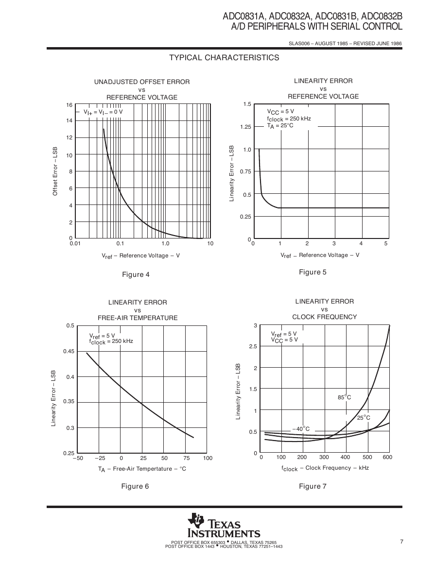
TYPICAL CHARACTERISTICS
UNADJUSTED OFFSET ERROR
vs
REFERENCE VOLTAGE
VI+ = VI – = 0 V
LINEARITY ERROR
vs
REFERENCE VOLTAGE
VCC = 5 V
fclock = 250 kHz
TA = 25°C
1.5
1.25
1.0
0.75
0.5
0.25
B
S
L
–
r
o
r
r
E
y
t
i
r
a
e
n
L
i
0
0.01
0.1
1.0
10
0
0
1
2
3
4
5
Vref – Reference Voltage – V
Vref – Reference Voltage – V
0.5
0.45
0.4
0.35
0.3
0.25
– 50
B
S
L
–
r
o
r
r
E
y
t
i
r
a
e
n
L
i
Figure 4
LINEARITY ERROR
vs
FREE-AIR TEMPERATURE
Vref = 5 V
fclock = 250 kHz
Figure 5
LINEARITY ERROR
vs
CLOCK FREQUENCY
Vref = 5 V
VCC = 5 V
85°C
25°C
– 40°C
3
2.5
2
1.5
1
0.5
B
S
L
–
r
o
r
r
E
y
t
i
r
a
e
n
L
i
0
75
– 25
TA – Free-Air Tempertature – °C
50
25
100
0
0
100
200
300
400
500
600
fclock – Clock Frequency – kHz
Figure 6
Figure 7
POST OFFICE BOX 655303 • DALLAS, TEXAS 75265
POST OFFICE BOX 1443 • HOUSTON, TEXAS 77251–1443
7
�
ADC0831A, ADC0832A, ADC0831B, ADC0832B
A/D PERIPHERALS WITH SERIAL CONTROL
SLAS006 – AUGUST 1985 – REVISED JUNE 1986
1.5
1
A
m
–
t
n
e
r
r
u
C
y
l
p
p
u
S
–
C
C
I
0.5
– 50
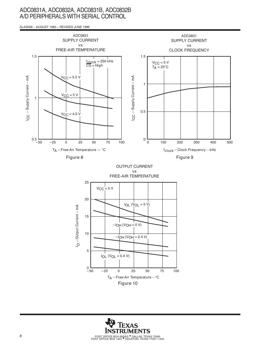
ADC0831
SUPPLY CURRENT
vs
CLOCK FREQUENCY
VCC = 5 V
TA = 25°C
ADC0831
SUPPLY CURRENT
vs
FREE-AIR TEMPERATURE
fclock = 250 kHz
CS = High
VCC = 5.5 V
VCC = 5 V
VCC = 4.5 V
1.5
1
0.5
A
m
–
t
n
e
r
r
u
C
y
l
p
p
u
S
–
C
C
I
0
– 25
TA – Free-Air Temperature — °C
50
25
Figure 8
75
100
0
0
100
200
300
400
500
fclock – Clock Frequency – kHz
Figure 9
A
m
–
t
n
e
r
r
u
C
t
u
p
t
u
O
–
O
I
OUTPUT CURRENT
vs
FREE-AIR TEMPERATURE
VCC = 5 V
IOL (VOL = 5 V)
– IOH (VOH = 0 V)
– IOH (VOH = 2.4 V)
25
20
15
10
5
IOL (VOL = 0.4 V)
0
– 50
– 25
0
25
50
75
100
TA – Free-Air Temperature – °C
Figure 10
8
POST OFFICE BOX 655303 • DALLAS, TEXAS 75265
POST OFFICE BOX 1443 • HOUSTON, TEXAS 77251–1443
�


 2023年江西萍乡中考道德与法治真题及答案.doc
 2012年重庆南川中考生物真题及答案.doc
 2013年江西师范大学地理学综合及文艺理论基础考研真题.doc
 2020年四川甘孜小升初语文真题及答案I卷.doc
 2020年注册岩土工程师专业基础考试真题及答案.doc
 2023-2024学年福建省厦门市九年级上学期数学月考试题及答案.doc
 2021-2022学年辽宁省沈阳市大东区九年级上学期语文期末试题及答案.doc
 2022-2023学年北京东城区初三第一学期物理期末试卷及答案.doc
 2018上半年江西教师资格初中地理学科知识与教学能力真题及答案.doc
 2012年河北国家公务员申论考试真题及答案-省级.doc
 2020-2021学年江苏省扬州市江都区邵樊片九年级上学期数学第一次质量检测试题及答案.doc
 2022下半年黑龙江教师资格证中学综合素质真题及答案.doc