logo资料库

TMS320C6713官方说明文档.pdf

第1页 / 共154页
第2页 / 共154页
第3页 / 共154页
第4页 / 共154页
第5页 / 共154页
第6页 / 共154页
第7页 / 共154页
第8页 / 共154页
资料共154页,剩余部分请下载后查看
SPRS294B - TMS320C6713B
Features
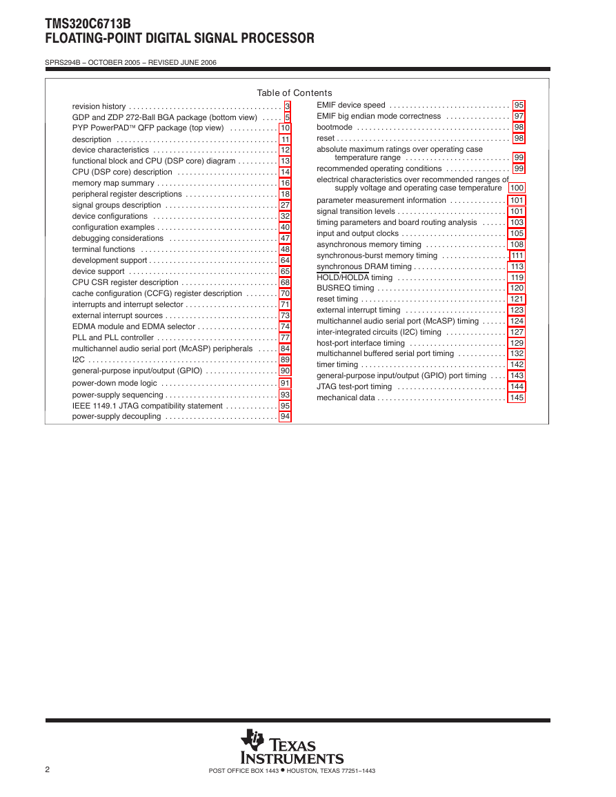
Table of Contents
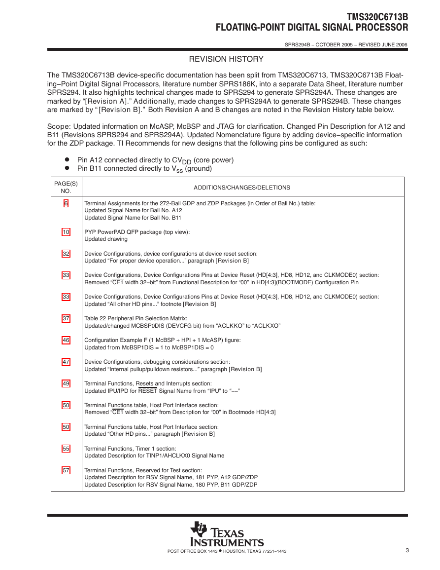
REVISION HISTORY
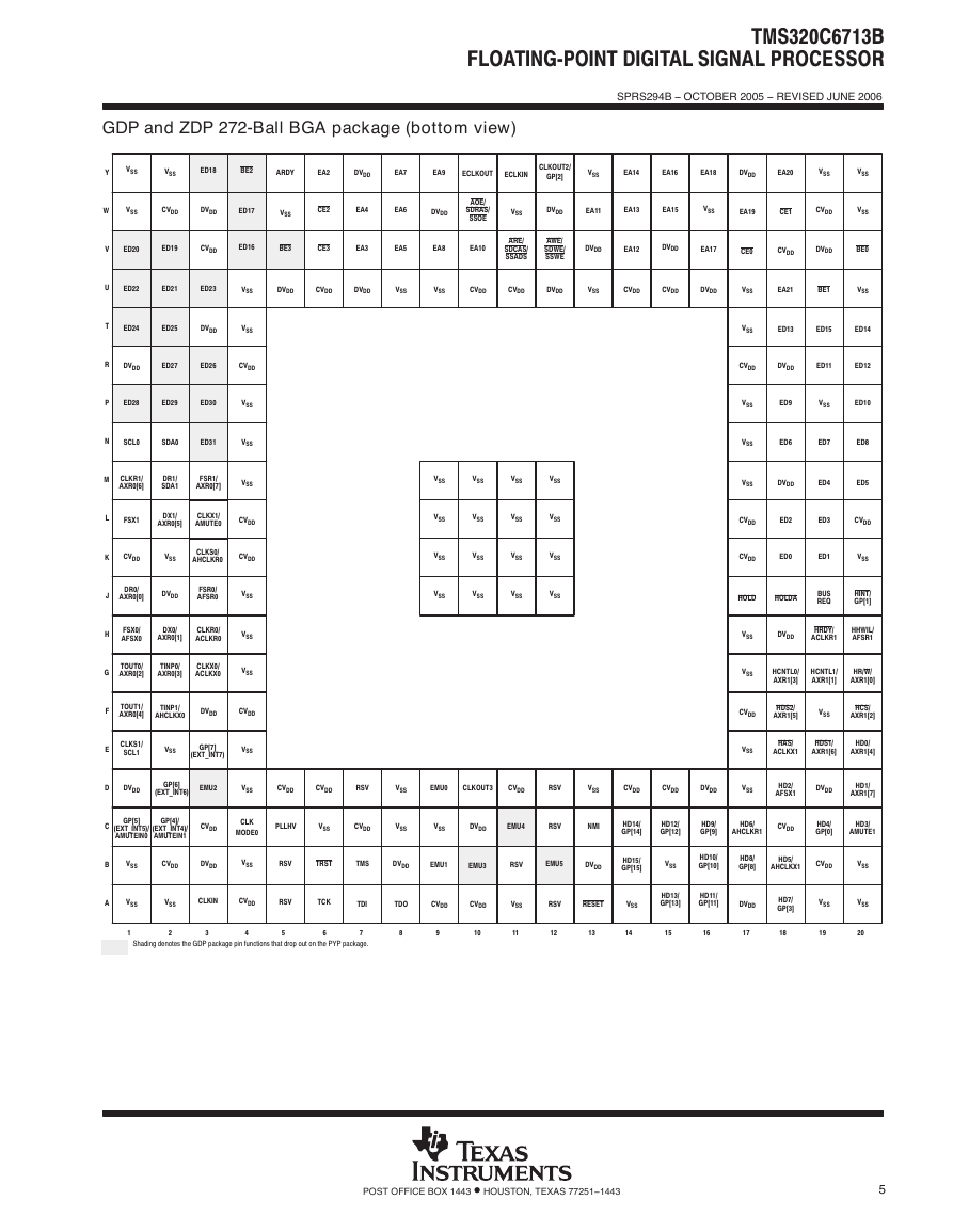
GDP and ZDP 272-Ball BGA package (bottom view)
PYP PowerPAD. QFP package (top view)
description
device characteristics
functional block and CPU (DSP core) diagram
CPU (DSP core) description
memory map summary
L2 memory structure expanded
peripheral register descriptions
signal groups description
DEVICE CONFIGURATIONS
device configurations at device reset
peripheral pin selection at device reset
peripheral selection/device configurations via the DEVCFG control register
multiplexed pins
configuration examples
debugging considerations
TERMINAL FUNCTIONS
Terminal Functions
development support
Software Development Tools:
Hardware Development Tools:
device support
device and development-support tool nomenclature
documentation support
CPU CSR register description
cache configuration (CCFG) register description
interrupts and interrupt selector
external interrupt sources
EDMA module and EDMA selector
ESEL0 Register (0x01A0 FF00)
ESEL1 Register (0x01A0 FF04)
ESEL3 Register (0x01A0 FF0C)
PLL and PLL controller
multichannel audio serial port (McASP) peripherals
McASP block diagram
multichannel time division multiplexed (TDM) synchronous transfer mode
burst transfer mode
supported bit stream formats for TDM and burst transfer modes
digital audio interface transmitter (DIT) transfer mode (transmitter only)
McASP flexible clock generators
McASP error handling and management
McASP interrupts and EDMA events
I2C
general-purpose input/output (GPIO)
power-down mode logic
triggering, wake-up, and effects
power-supply sequencing
system-level design considerations
power-supply design considerations
power-supply decoupling
IEEE 1149.1 JTAG compatibility statement
EMIF device speed
EMIF big endian mode correctness
bootmode
reset
absolute maximum ratings over operating case temperature range (unless otherwise noted)†
recommended operating conditions†
electrical characteristics over recommended ranges of supply voltage and operating case temperature† ( unless otherwise noted)
PARAMETER MEASUREMENT INFORMATION
signal transition levels
AC transient rise/fall time specifications
timing parameters and board routing analysis
INPUT AND OUTPUT CLOCKS
timing requirements for CLKIN for PYP-200 and GDP/ZDP-225†‡§ (see Figure 31)
timing requirements for CLKIN for PYP-225 and GDP/ZDP-300 †‡§ (see Figure 31)
timing requirements for CLKIN for PYPA-167, GDPA/ZDPA-200 and PYPA-200†‡§ (see Figure 31)
switching characteristics over recommended operating conditions for CLKOUT2†‡ ( see Figure 32)
switching characteristics over recommended operating conditions for CLKOUT3†§ (see Figure 33)
timing requirements for ECLKIN† (see Figure 34)
switching characteristics over recommended operating conditions for ECLKOUT‡§# (see Figure 35)
ASYNCHRONOUS MEMORY TIMING
timing requirements for asynchronous memory cycles†‡§ (see Figure 36-Figure 37)
switching characteristics over recommended operating conditions for asynchronous memory cyclesद (see Figure 36-Figure 37)
SYNCHRONOUS-BURST MEMORY TIMING
timing requirements for synchronous-burst SRAM cycles† (see Figure 38)
switching characteristics over recommended operating conditions for synchronous-burst SRAM cycles†‡ ( see Figure 38 and Figure 39)
SYNCHRONOUS DRAM TIMING
timing requirements for synchronous DRAM cycles† (see Figure 40)
switching characteristics over recommended operating conditions for synchronous DRAM cycles†‡ ( see Figure 40- Figure 46)
HOLD\/HOLDA\ TIMING
timing requirements for the HOLD\/HOLDA\ cycles† (see Figure 47)
switching characteristics over recommended operating conditions for the HOLD\/HOLDA\ cycles†‡ ( see Figure 47)
BUSREQ TIMING
switching characteristics over recommended operating conditions for the BUSREQ cycles ( see Figure 48)
RESET TIMING
timing requirements for reset†‡ (see Figure 49)
switching characteristics over recommended operating conditions during reset¶ (see Figure 49)
EXTERNAL INTERRUPT TIMING
timing requirements for external interrupts† (see Figure 50)
MULTICHANNEL AUDIO SERIAL PORT (McASP) TIMING
timing requirements for McASP (see Figure 51 and Figure 52)
switching characteristics over recommended operating conditions for McASP‡ (see Figure 51 and Figure 52)
INTER-INTEGRATED CIRCUITS (I2C) TIMING
timing requirements for I2C timings† ( see Figure 53)
switching characteristics for I2C timings† (see Figure 54)
HOST-PORT INTERFACE TIMING
timing requirements for host-port interface cycles†‡ ( see Figure 55, Figure 56, Figure 57, and Figure 58)
switching characteristics over recommended operating conditions during host-port interface cycles†‡ ( see Figure 55, Figure 56, Figure 57, and Figure 58)
MULTICHANNEL BUFFERED SERIAL PORT TIMING
timing requirements for McBSP†‡ (see Figure 59)
switching characteristics over recommended operating conditions for McBSP†‡ (see Figure 59)
timing requirements for FSR when GSYNC = 1 (see Figure 60)
timing requirements for McBSP as SPI master or slave: CLKSTP = 10b, CLKXP = 0†‡ (see Figure 61)
switching characteristics over recommended operating conditions for McBSP as SPI master or slave: CLKSTP = 10b, CLKXP = 0†‡ ( see Figure 61)
timing requirements for McBSP as SPI master or slave: CLKSTP = 11b, CLKXP = 0†‡ (see Figure 62)
switching characteristics over recommended operating conditions for McBSP as SPI master or slave: CLKSTP = 11b, CLKXP = 0†‡ ( see Figure 62)
timing requirements for McBSP as SPI master or slave: CLKSTP = 10b, CLKXP = 1†‡ (see Figure 63)
switching characteristics over recommended operating conditions for McBSP as SPI master or slave: CLKSTP = 10b, CLKXP = 1†‡ ( see Figure 63)
timing requirements for McBSP as SPI master or slave: CLKSTP = 11b, CLKXP = 1†‡ (see Figure 64)
switching characteristics over recommended operating conditions for McBSP as SPI master or slave: CLKSTP = 11b, CLKXP = 1†‡ ( see Figure 64)
TIMER TIMING
timing requirements for timer inputs† (see Figure 65)
switching characteristics over recommended operating conditions for timer outputs† ( see Figure 65)
GENERAL-PURPOSE INPUT/OUTPUT (GPIO) PORT TIMING
timing requirements for GPIO inputs†‡ (see Figure 66)
switching characteristics over recommended operating conditions for GPIO outputs†§ (see Figure 66)
JTAG TEST-PORT TIMING
timing requirements for JTAG test port (see Figure 67)
switching characteristics over recommended operating conditions for JTAG test port ( see Figure 67)
MECHANICAL DATA
thermal resistance characteristics (S-PBGA package) for GDP
thermal resistance characteristics (S-PBGA package) for ZDP
thermal resistance characteristics (S-PQFP-G208 package) for PYP
packaging information
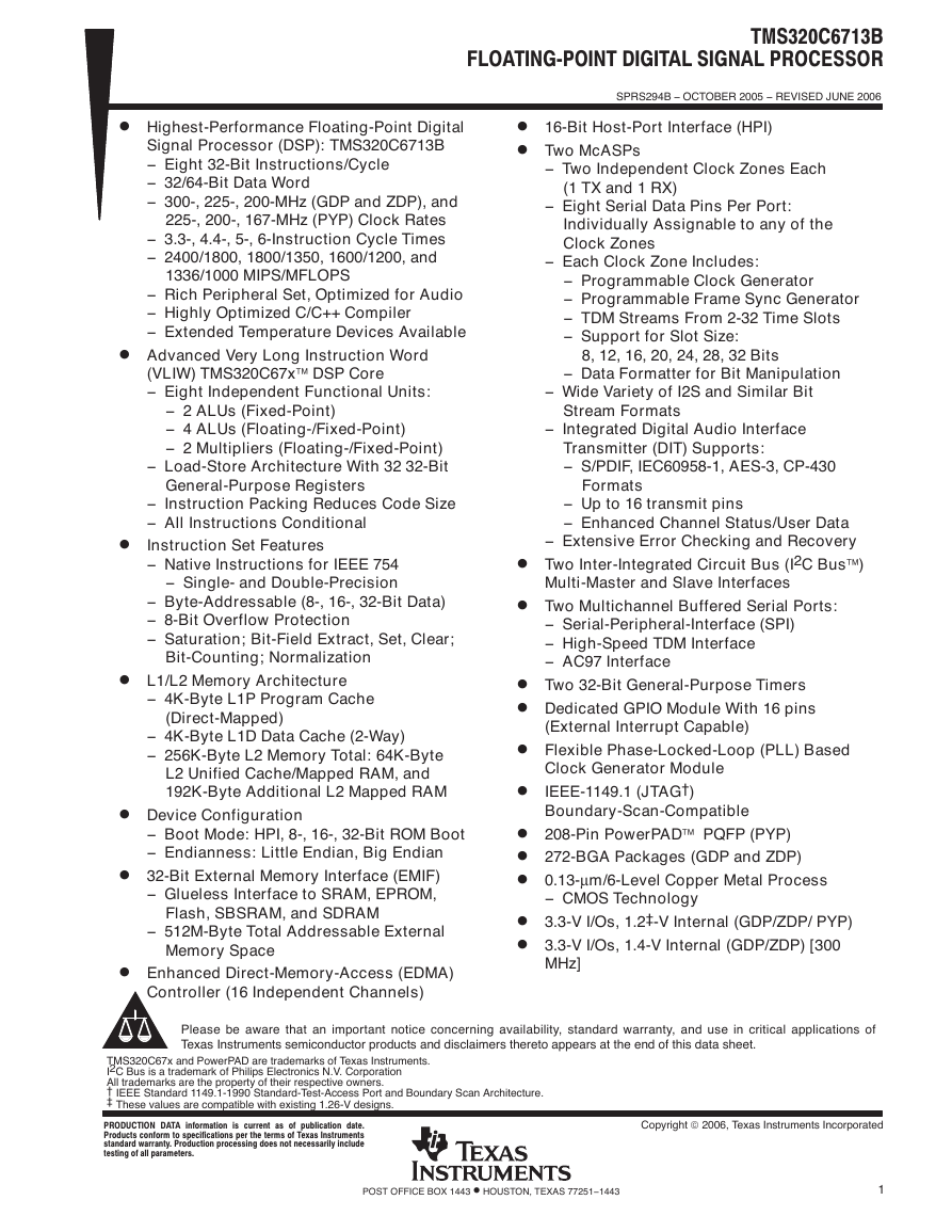
TMS320C6713B FLOATINGĆPOINT DIGITAL SIGNAL PROCESSOR SPRS294B − OCTOBER 2005 − REVISED JUNE 2006 D Highest-Performance Floating-Point Digital Signal Processor (DSP): TMS320C6713B − Eight 32-Bit Instructions/Cycle − 32/64-Bit Data Word − 300-, 225-, 200-MHz (GDP and ZDP), and 225-, 200-, 167-MHz (PYP) Clock Rates − 3.3-, 4.4-, 5-, 6-Instruction Cycle Times − 2400/1800, 1800/1350, 1600/1200, and 1336/1000 MIPS/MFLOPS − Rich Peripheral Set, Optimized for Audio − Highly Optimized C/C++ Compiler − Extended Temperature Devices Available D Advanced Very Long Instruction Word (VLIW) TMS320C67x DSP Core − Eight Independent Functional Units: − 2 ALUs (Fixed-Point) − 4 ALUs (Floating-/Fixed-Point) − 2 Multipliers (Floating-/Fixed-Point) − Load-Store Architecture With 32 32-Bit General-Purpose Registers − Instruction Packing Reduces Code Size − All Instructions Conditional D Instruction Set Features − Native Instructions for IEEE 754 − Single- and Double-Precision − Byte-Addressable (8-, 16-, 32-Bit Data) − 8-Bit Overflow Protection − Saturation; Bit-Field Extract, Set, Clear; Bit-Counting; Normalization D L1/L2 Memory Architecture − 4K-Byte L1P Program Cache (Direct-Mapped) − 4K-Byte L1D Data Cache (2-Way) − 256K-Byte L2 Memory Total: 64K-Byte L2 Unified Cache/Mapped RAM, and 192K-Byte Additional L2 Mapped RAM D Device Configuration − Boot Mode: HPI, 8-, 16-, 32-Bit ROM Boot − Endianness: Little Endian, Big Endian D 32-Bit External Memory Interface (EMIF) − Glueless Interface to SRAM, EPROM, Flash, SBSRAM, and SDRAM − 512M-Byte Total Addressable External Memory Space D Enhanced Direct-Memory-Access (EDMA) Controller (16 Independent Channels) D 16-Bit Host-Port Interface (HPI) D Two McASPs − Two Independent Clock Zones Each (1 TX and 1 RX) − Eight Serial Data Pins Per Port: Individually Assignable to any of the Clock Zones − Each Clock Zone Includes: − Programmable Clock Generator − Programmable Frame Sync Generator − TDM Streams From 2-32 Time Slots − Support for Slot Size: 8, 12, 16, 20, 24, 28, 32 Bits − Data Formatter for Bit Manipulation − Wide Variety of I2S and Similar Bit Stream Formats − Integrated Digital Audio Interface Transmitter (DIT) Supports: − S/PDIF, IEC60958-1, AES-3, CP-430 Formats − Up to 16 transmit pins − Enhanced Channel Status/User Data − Extensive Error Checking and Recovery D Two Inter-Integrated Circuit Bus (I2C Bus) Multi-Master and Slave Interfaces D Two Multichannel Buffered Serial Ports: − Serial-Peripheral-Interface (SPI) − High-Speed TDM Interface − AC97 Interface D Two 32-Bit General-Purpose Timers D Dedicated GPIO Module With 16 pins (External Interrupt Capable) D Flexible Phase-Locked-Loop (PLL) Based Clock Generator Module D IEEE-1149.1 (JTAG†) Boundary-Scan-Compatible D 208-Pin PowerPAD PQFP (PYP) D 272-BGA Packages (GDP and ZDP) D 0.13-µm/6-Level Copper Metal Process − CMOS Technology D 3.3-V I/Os, 1.2‡-V Internal (GDP/ZDP/ PYP) D 3.3-V I/Os, 1.4-V Internal (GDP/ZDP) [300 MHz] Please be aware that an important notice concerning availability, standard warranty, and use in critical applications of Texas Instruments semiconductor products and disclaimers thereto appears at the end of this data sheet. TMS320C67x and PowerPAD are trademarks of Texas Instruments. I2C Bus is a trademark of Philips Electronics N.V. Corporation All trademarks are the property of their respective owners. † IEEE Standard 1149.1-1990 Standard-Test-Access Port and Boundary Scan Architecture. ‡ These values are compatible with existing 1.26-V designs. information PRODUCTION DATA is current as of publication date. Products conform to specifications per the terms of Texas Instruments standard warranty. Production processing does not necessarily include testing of all parameters. Copyright  2006, Texas Instruments Incorporated POST OFFICE BOX 1443 • HOUSTON, TEXAS 77251−1443 1
TMS320C6713B FLOATINGĆPOINT DIGITAL SIGNAL PROCESSOR SPRS294B − OCTOBER 2005 − REVISED JUNE 2006 Table of Contents revision history GDP and ZDP 272-Ball BGA package (bottom view) PYP PowerPAD QFP package (top view) description device characteristics functional block and CPU (DSP core) diagram CPU (DSP core) description memory map summary peripheral register descriptions signal groups description device configurations configuration examples debugging considerations terminal functions development support device support CPU CSR register description cache configuration (CCFG) register description interrupts and interrupt selector external interrupt sources EDMA module and EDMA selector PLL and PLL controller multichannel audio serial port (McASP) peripherals I2C general-purpose input/output (GPIO) power-down mode logic power-supply sequencing IEEE 1149.1 JTAG compatibility statement power-supply decoupling . . . . . . . . . . . . . . . . . . . . . . . . . . . . . . . . . . . . . . . . . . . . . . . . . . . . . . . . . . . . . . . . . . . . . . . . . . . . . . . . . . . . . . . . . . . . . . . . . . . . . . . . . . . . . . . . . . . . . . . . . . . . . . . . . . . . . . . . . . . . . . . . . . . . . . . . . . . . . . . . . . . . . . . . . . . . . . . . . . . . . . . . . . . . . . . . . . . . . . . . . . . . . . . . . . . . . . . . . . . . . . . . . . . . . . . . . . . . . . . . . . . . . . . . . . . . . . . . . . . . . . . . . . . . . . . . . . . . . . . . . . . . . . . . . . . . . . . . . . . . . . . . . . . . . . . . . . . . . . . . . . . . . . . . . . . . . . . . . . . . . . . . . . . . . . . . . . . . . . . . . . . . . . . . . . . . . . . . . . . . . . . . . . . . . . . . . . . . . . . . . . . . . . . . . . . . . . . . . . . . . . . . . . . . . . . . . . . . . . . . . . . . . . . . . . . . . . . . . . . . . . . . . . . . . . . . . . . . . . . . . . . . . . . . . . . . . . . . . . . . . . . . . . . . . . . . . . . . . . . . . . . . . . . . . . . . . . . . . . . . . . . . . . . . . . . . . . . . . . . . . . . . . . . . . . . . . . . . . . . . . . . . . . . . . . . . . . . . . . . . . . . . . . . . . . . . . . . . . . . . . . . . . . . . . . . . . . . . . . . . . . . . . . . . . . . . . . . . . . . . . . . . . . . . . . . . . . . . . . . . . . . . . . . . . . . . . . . . . . . . . . . . . . . . . . . . . . . . . . . . . . . . . . . . . . . . . . 3 5 10 11 12 13 14 16 18 27 32 40 47 48 64 65 68 70 71 73 74 77 84 89 90 91 93 95 94 . . . . . . . . . . . . . . . . . . . . . . . . . . . . . . . . . . . . . . . . . . . . . . . . . . . . . . . . . . . . . . . . . . . . . . . . . . . . . . . . . . . . . . . . . . . . . . . . . . . . . . . . . . . . . . . . . . . . . . . . . . . . . . . EMIF device speed EMIF big endian mode correctness bootmode reset absolute maximum ratings over operating case 95 97 98 98 99 99 temperature range . . . . . . . . . . . . . . . . . . . . . . . . . . recommended operating conditions . . . . . . . . . . . . . . . . electrical characteristics over recommended ranges of supply voltage and operating case temperature 100 101 101 103 105 108 111 113 119 120 121 123 124 127 129 132 142 143 144 145 parameter measurement information signal transition levels timing parameters and board routing analysis input and output clocks asynchronous memory timing synchronous-burst memory timing synchronous DRAM timing HOLD/HOLDA timing BUSREQ timing reset timing external interrupt timing multichannel audio serial port (McASP) timing inter-integrated circuits (I2C) timing host-port interface timing multichannel buffered serial port timing timer timing general-purpose input/output (GPIO) port timing JTAG test-port timing mechanical data . . . . . . . . . . . . . . . . . . . . . . . . . . . . . . . . . . . . . . . . . . . . . . . . . . . . . . . . . . . . . . . . . . . . . . . . . . . . . . . . . . . . . . . . . . . . . . . . . . . . . . . . . . . . . . . . . . . . . . . . . . . . . . . . . . . . . . . . . . . . . . . . . . . . . . . . . . . . . . . . . . . . . . . . . . . . . . . . . . . . . . . . . . . . . . . . . . . . . . . . . . . . . . . . . . . . . . . . . . . . . . . . . . . . . . . . . . . . . . . . . . . . . . . . . . . . . . . . . . . . . . . . . . . . . . . . . . . . . . . . . . . . . . . . . . . . . . . . . . . . . . . . . . . . . . . . . . . . . . . . . . . . . . . . . . . . . . . . . . . . . . . . . . . . . . . . . . . . . . . . . . . . . . . . . . . . . . . . . . . . . . . . . . . . . . . . . . . . . . . . . . . . . . . . . 2 POST OFFICE BOX 1443 • HOUSTON, TEXAS 77251−1443
TMS320C6713B FLOATINGĆPOINT DIGITAL SIGNAL PROCESSOR SPRS294B − OCTOBER 2005 − REVISED JUNE 2006 REVISION HISTORY The TMS320C6713B device-specific documentation has been split from TMS320C6713, TMS320C6713B Float- ing−Point Digital Signal Processors, literature number SPRS186K, into a separate Data Sheet, literature number SPRS294. It also highlights technical changes made to SPRS294 to generate SPRS294A. These changes are marked by “[Revision A].” Additionally, made changes to SPRS294A to generate SPRS294B. These changes are marked by “[Revision B].” Both Revision A and B changes are noted in the Revision History table below. Scope: Updated information on McASP, McBSP and JTAG for clarification. Changed Pin Description for A12 and B11 (Revisions SPRS294 and SPRS294A). Updated Nomenclature figure by adding device−specific information for the ZDP package. TI Recommends for new designs that the following pins be configured as such: D Pin A12 connected directly to CVDD (core power) D Pin B11 connected directly to Vss (ground) PAGE(S) NO. ADDITIONS/CHANGES/DELETIONS 6 10 32 33 33 37 46 47 49 50 50 55 57 Terminal Assignments for the 272-Ball GDP and ZDP Packages (in Order of Ball No.) table: Updated Signal Name for Ball No. A12 Updated Signal Name for Ball No. B11 PYP PowerPAD QFP package (top view): Updated drawing Device Configurations, device configurations at device reset section: Updated “For proper device operation...” paragraph [Revision B] Device Configurations, Device Configurations Pins at Device Reset (HD[4:3], HD8, HD12, and CLKMODE0) section: Removed “CE1 width 32−bit” from Functional Description for “00” in HD[4:3](BOOTMODE) Configuration Pin Device Configurations, Device Configurations Pins at Device Reset (HD[4:3], HD8, HD12, and CLKMODE0) section: Updated “All other HD pins...” footnote [Revision B] Table 22 Peripheral Pin Selection Matrix: Updated/changed MCBSP0DIS (DEVCFG bit) from “ACLKKO” to “ACLKXO” Configuration Example F (1 McBSP + HPI + 1 McASP) figure: Updated from McBSP1DIS = 1 to McBSP1DIS = 0 Device Configurations, debugging considerations section: Updated “Internal pullup/pulldown resistors...” paragraph [Revision B] Terminal Functions, Resets and Interrupts section: Updated IPU/IPD for RESET Signal Name from “IPU” to “−−” Terminal Functions table, Host Port Interface section: Removed “CE1 width 32−bit” from Description for “00” in Bootmode HD[4:3] Terminal Functions table, Host Port Interface section: Updated “Other HD pins...” paragraph [Revision B] Terminal Functions, Timer 1 section: Updated Description for TINP1/AHCLKX0 Signal Name Terminal Functions, Reserved for Test section: Updated Description for RSV Signal Name, 181 PYP, A12 GDP/ZDP Updated Description for RSV Signal Name, 180 PYP, B11 GDP/ZDP POST OFFICE BOX 1443 • HOUSTON, TEXAS 77251−1443 3
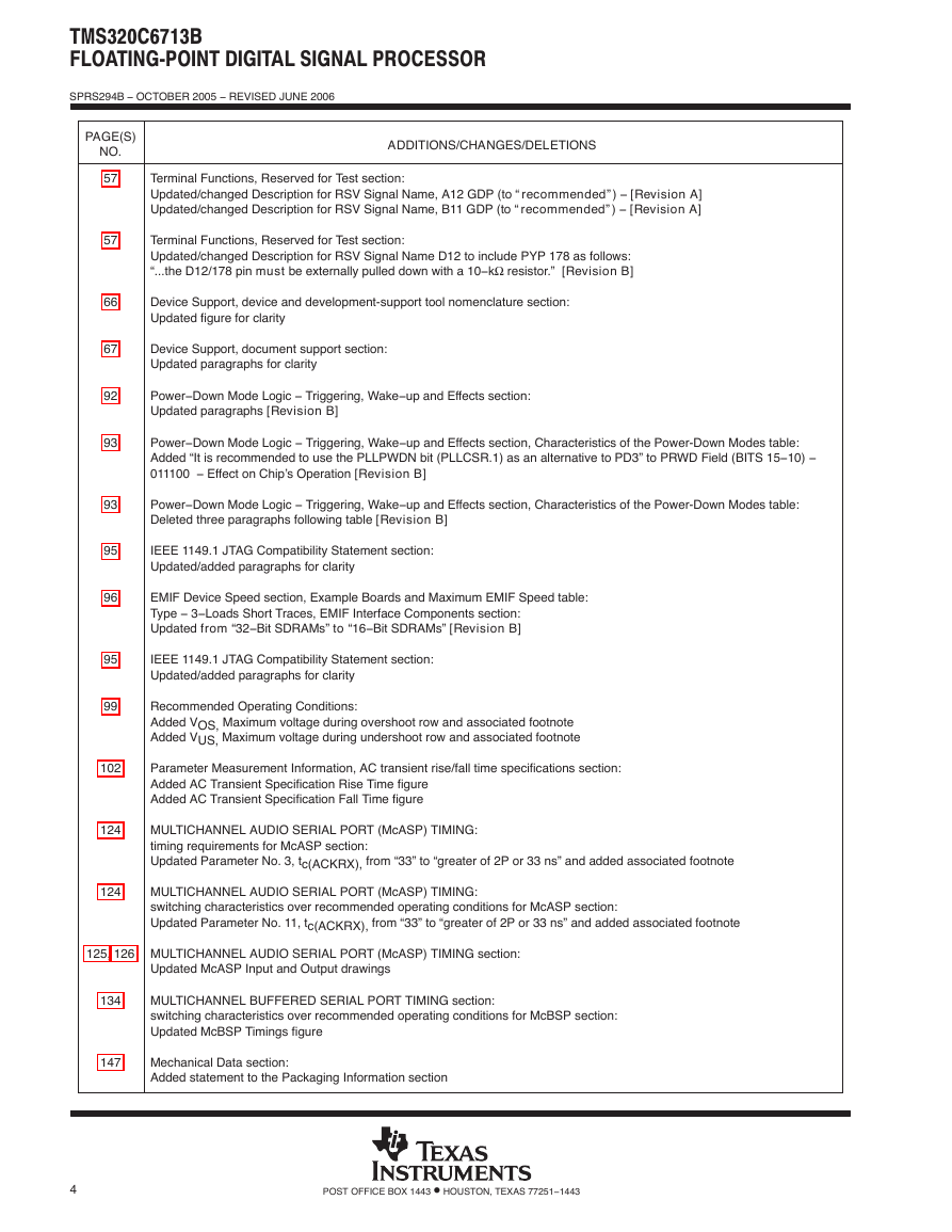
TMS320C6713B FLOATINGĆPOINT DIGITAL SIGNAL PROCESSOR SPRS294B − OCTOBER 2005 − REVISED JUNE 2006 PAGE(S) NO. 57 57 66 67 92 93 93 95 96 95 99 102 124 124 ADDITIONS/CHANGES/DELETIONS Terminal Functions, Reserved for Test section: Updated/changed Description for RSV Signal Name, A12 GDP (to “recommended”) − [Revision A] Updated/changed Description for RSV Signal Name, B11 GDP (to “recommended”) − [Revision A] Terminal Functions, Reserved for Test section: Updated/changed Description for RSV Signal Name D12 to include PYP 178 as follows: “...the D12/178 pin must be externally pulled down with a 10−kΩ resistor.” [Revision B] Device Support, device and development-support tool nomenclature section: Updated figure for clarity Device Support, document support section: Updated paragraphs for clarity Power−Down Mode Logic − Triggering, Wake−up and Effects section: Updated paragraphs [Revision B] Power−Down Mode Logic − Triggering, Wake−up and Effects section, Characteristics of the Power-Down Modes table: Added “It is recommended to use the PLLPWDN bit (PLLCSR.1) as an alternative to PD3” to PRWD Field (BITS 15−10) − 011100 − Effect on Chip’s Operation [Revision B] Power−Down Mode Logic − Triggering, Wake−up and Effects section, Characteristics of the Power-Down Modes table: Deleted three paragraphs following table [Revision B] IEEE 1149.1 JTAG Compatibility Statement section: Updated/added paragraphs for clarity EMIF Device Speed section, Example Boards and Maximum EMIF Speed table: Type − 3−Loads Short Traces, EMIF Interface Components section: Updated from “32−Bit SDRAMs” to “16−Bit SDRAMs” [Revision B] IEEE 1149.1 JTAG Compatibility Statement section: Updated/added paragraphs for clarity Recommended Operating Conditions: Added VOS, Maximum voltage during overshoot row and associated footnote Added VUS, Maximum voltage during undershoot row and associated footnote Parameter Measurement Information, AC transient rise/fall time specifications section: Added AC Transient Specification Rise Time figure Added AC Transient Specification Fall Time figure MULTICHANNEL AUDIO SERIAL PORT (McASP) TIMING: timing requirements for McASP section: Updated Parameter No. 3, tc(ACKRX), from “33” to “greater of 2P or 33 ns” and added associated footnote MULTICHANNEL AUDIO SERIAL PORT (McASP) TIMING: switching characteristics over recommended operating conditions for McASP section: Updated Parameter No. 11, tc(ACKRX), from “33” to “greater of 2P or 33 ns” and added associated footnote 125, 126 MULTICHANNEL AUDIO SERIAL PORT (McASP) TIMING section: Updated McASP Input and Output drawings 134 147 MULTICHANNEL BUFFERED SERIAL PORT TIMING section: switching characteristics over recommended operating conditions for McBSP section: Updated McBSP Timings figure Mechanical Data section: Added statement to the Packaging Information section 4 POST OFFICE BOX 1443 • HOUSTON, TEXAS 77251−1443
TMS320C6713B FLOATINGĆPOINT DIGITAL SIGNAL PROCESSOR SPRS294B − OCTOBER 2005 − REVISED JUNE 2006 GDP and ZDP 272-Ball BGA package (bottom view) Y VSS VSS ED18 BE2 ARDY EA2 DVDD EA7 EA9 ECLKOUT ECLKIN CLKOUT2/ GP[2] VSS EA14 EA16 EA18 DVDD EA20 VSS VSS W VSS CVDD DVDD ED17 VSS CE2 EA4 EA6 DVDD AOE/ SDRAS/ SSOE VSS DVDD EA11 EA13 EA15 VSS EA19 CE1 CVDD VSS V ED20 ED19 CVDD ED16 BE3 CE3 EA3 EA5 EA8 EA10 ARE/ SDCAS/ SSADS AWE/ SDWE/ SSWE DVDD EA12 DVDD EA17 CE0 CVDD DVDD BE0 U ED22 ED21 ED23 VSS DVDD CVDD DVDD VSS VSS CVDD CVDD DVDD VSS CVDD CVDD DVDD VSS EA21 BE1 VSS T R ED24 ED25 DVDD VSS DVDD ED27 ED26 CVDD P ED28 ED29 ED30 N SCL0 SDA0 ED31 M CLKR1/ AXR0[6] DR1/ SDA1 FSR1/ AXR0[7] VSS VSS VSS L FSX1 DX1/ AXR0[5] CLKX1/ AMUTE0 CVDD K CVDD VSS CLKS0/ AHCLKR0 CVDD DR0/ AXR0[0] DVDD FSR0/ AFSR0 FSX0/ AFSX0 DX0/ AXR0[1] CLKR0/ ACLKR0 TOUT0/ AXR0[2] TINP0/ AXR0[3] CLKX0/ ACLKX0 VSS VSS VSS TOUT1/ AXR0[4] TINP1/ AHCLKX0 DVDD CVDD CLKS1/ SCL1 VSS GP[7] (EXT_INT7) VSS VSS ED13 ED15 ED14 CVDD DVDD ED11 ED12 VSS ED9 VSS ED10 VSS ED6 ED7 ED8 VSS VSS VSS VSS VSS DVDD ED4 ED5 VSS VSS VSS VSS CVDD ED2 ED3 CVDD VSS VSS VSS VSS CVDD ED0 ED1 VSS VSS VSS VSS VSS HOLD HOLDA BUS REQ HINT/ GP[1] VSS DVDD HRDY/ ACLKR1 HHWIL/ AFSR1 VSS HCNTL0/ AXR1[3] HCNTL1/ AXR1[1] HR/W/ AXR1[0] CVDD HDS2/ AXR1[5] VSS HCS/ AXR1[2] VSS HAS/ ACLKX1 HDS1/ AXR1[6] HD0/ AXR1[4] J H G F E D C B A DVDD GP[6] (EXT_INT6) EMU2 VSS CVDD CVDD RSV VSS EMU0 CLKOUT3 CVDD RSV VSS CVDD CVDD DVDD VSS HD2/ AFSX1 DVDD HD1/ AXR1[7] GP[5] GP[4]/ (EXT_INT5)/ AMUTEIN0 (EXT_INT4)/ AMUTEIN1 CVDD CLK MODE0 PLLHV VSS CVDD VSS VSS DVDD EMU4 RSV NMI HD14/ GP[14] HD12/ GP[12] HD9/ GP[9] HD6/ AHCLKR1 CVDD HD4/ GP[0] HD3/ AMUTE1 VSS CVDD DVDD VSS RSV TRST TMS DVDD EMU1 EMU3 RSV EMU5 DVDD HD15/ GP[15] VSS HD10/ GP[10] HD8/ GP[8] HD5/ AHCLKX1 CVDD VSS VSS VSS CLKIN CVDD RSV TCK TDI TDO CVDD CVDD VSS RSV RESET VSS HD13/ GP[13] HD11/ GP[11] DVDD HD7/ GP[3] VSS VSS 1 2 3 4 5 6 7 8 9 10 11 12 13 14 15 16 17 18 19 20 Shading denotes the GDP package pin functions that drop out on the PYP package. POST OFFICE BOX 1443 • HOUSTON, TEXAS 77251−1443 5
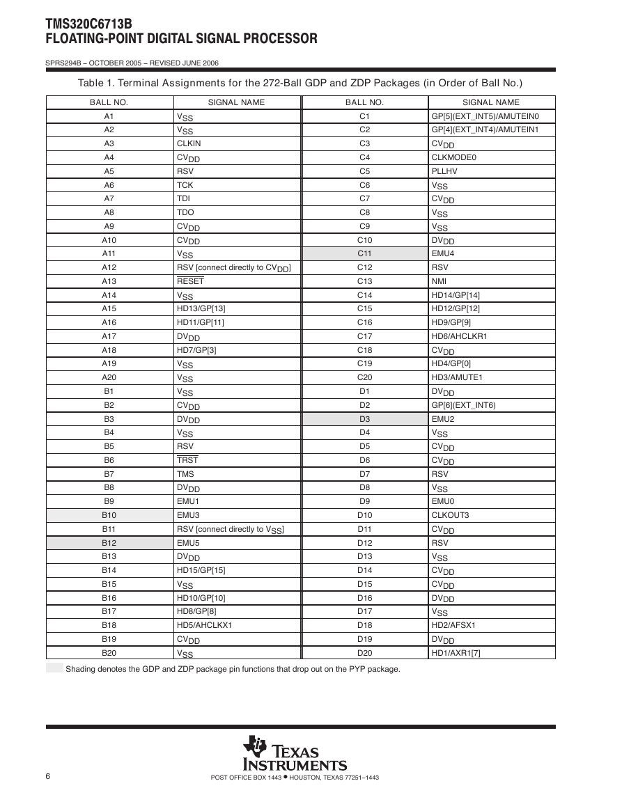
TMS320C6713B FLOATINGĆPOINT DIGITAL SIGNAL PROCESSOR SPRS294B − OCTOBER 2005 − REVISED JUNE 2006 Table 1. Terminal Assignments for the 272-Ball GDP and ZDP Packages (in Order of Ball No.) BALL NO. SIGNAL NAME BALL NO. SIGNAL NAME A1 A2 A3 A4 A5 A6 A7 A8 A9 A10 A11 A12 A13 A14 A15 A16 A17 A18 A19 A20 B1 B2 B3 B4 B5 B6 B7 B8 B9 B10 B11 B12 B13 B14 B15 B16 B17 B18 B19 B20 VSS VSS CLKIN CVDD RSV TCK TDI TDO CVDD CVDD VSS RSV [connect directly to CVDD] RESET VSS HD13/GP[13] HD11/GP[11] DVDD HD7/GP[3] VSS VSS VSS CVDD DVDD VSS RSV TRST TMS DVDD EMU1 EMU3 RSV [connect directly to VSS] EMU5 DVDD HD15/GP[15] VSS HD10/GP[10] HD8/GP[8] HD5/AHCLKX1 CVDD VSS C1 C2 C3 C4 C5 C6 C7 C8 C9 C10 C11 C12 C13 C14 C15 C16 C17 C18 C19 C20 D1 D2 D3 D4 D5 D6 D7 D8 D9 D10 D11 D12 D13 D14 D15 D16 D17 D18 D19 D20 GP[5](EXT_INT5)/AMUTEIN0 GP[4](EXT_INT4)/AMUTEIN1 CVDD CLKMODE0 PLLHV VSS CVDD VSS VSS DVDD EMU4 RSV NMI HD14/GP[14] HD12/GP[12] HD9/GP[9] HD6/AHCLKR1 CVDD HD4/GP[0] HD3/AMUTE1 DVDD GP[6](EXT_INT6) EMU2 VSS CVDD CVDD RSV VSS EMU0 CLKOUT3 CVDD RSV VSS CVDD CVDD DVDD VSS HD2/AFSX1 DVDD HD1/AXR1[7] Shading denotes the GDP and ZDP package pin functions that drop out on the PYP package. 6 POST OFFICE BOX 1443 • HOUSTON, TEXAS 77251−1443
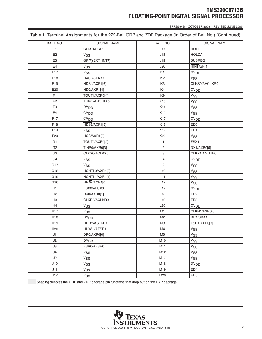
TMS320C6713B FLOATINGĆPOINT DIGITAL SIGNAL PROCESSOR SPRS294B − OCTOBER 2005 − REVISED JUNE 2006 Table 1. Terminal Assignments for the 272-Ball GDP and ZDP Package (in Order of Ball No.) (Continued) BALL NO. SIGNAL NAME BALL NO. SIGNAL NAME E1 E2 E3 E4 E17 E18 E19 E20 F1 F2 F3 F4 F17 F18 F19 F20 G1 G2 G3 G4 G17 G18 G19 G20 H1 H2 H3 H4 H17 H18 H19 H20 J1 J2 J3 J4 J9 J10 J11 J12 CLKS1/SCL1 VSS GP[7](EXT_INT7) VSS VSS HAS/ACLKX1 HDS1/AXR1[6] HD0/AXR1[4] TOUT1/AXR0[4] TINP1/AHCLKX0 DVDD CVDD CVDD HDS2/AXR1[5] VSS HCS/AXR1[2] TOUT0/AXR0[2] TINP0/AXR0[3] CLKX0/ACLKX0 VSS VSS HCNTL0/AXR1[3] HCNTL1/AXR1[1] HR/W/AXR1[0] FSX0/AFSX0 DX0/AXR0[1] CLKR0/ACLKR0 VSS VSS DVDD HRDY/ACLKR1 HHWIL/AFSR1 DR0/AXR0[0] DVDD FSR0/AFSR0 VSS VSS VSS VSS VSS J17 J18 J19 J20 K1 K2 K3 K4 K9 K10 K11 K12 K17 K18 K19 K20 L1 L2 L3 L4 L9 L10 L11 L12 L17 L18 L19 L20 M1 M2 M3 M4 M9 M10 M11 M12 M17 M18 M19 M20 HOLD HOLDA BUSREQ HINT/GP[1] CVDD VSS CLKS0/AHCLKR0 CVDD VSS VSS VSS VSS CVDD ED0 ED1 VSS FSX1 DX1/AXR0[5] CLKX1/AMUTE0 CVDD VSS VSS VSS VSS CVDD ED2 ED3 CVDD CLKR1/AXR0[6] DR1/SDA1 FSR1/AXR0[7] VSS VSS VSS VSS VSS VSS DVDD ED4 ED5 Shading denotes the GDP and ZDP package pin functions that drop out on the PYP package. POST OFFICE BOX 1443 • HOUSTON, TEXAS 77251−1443 7
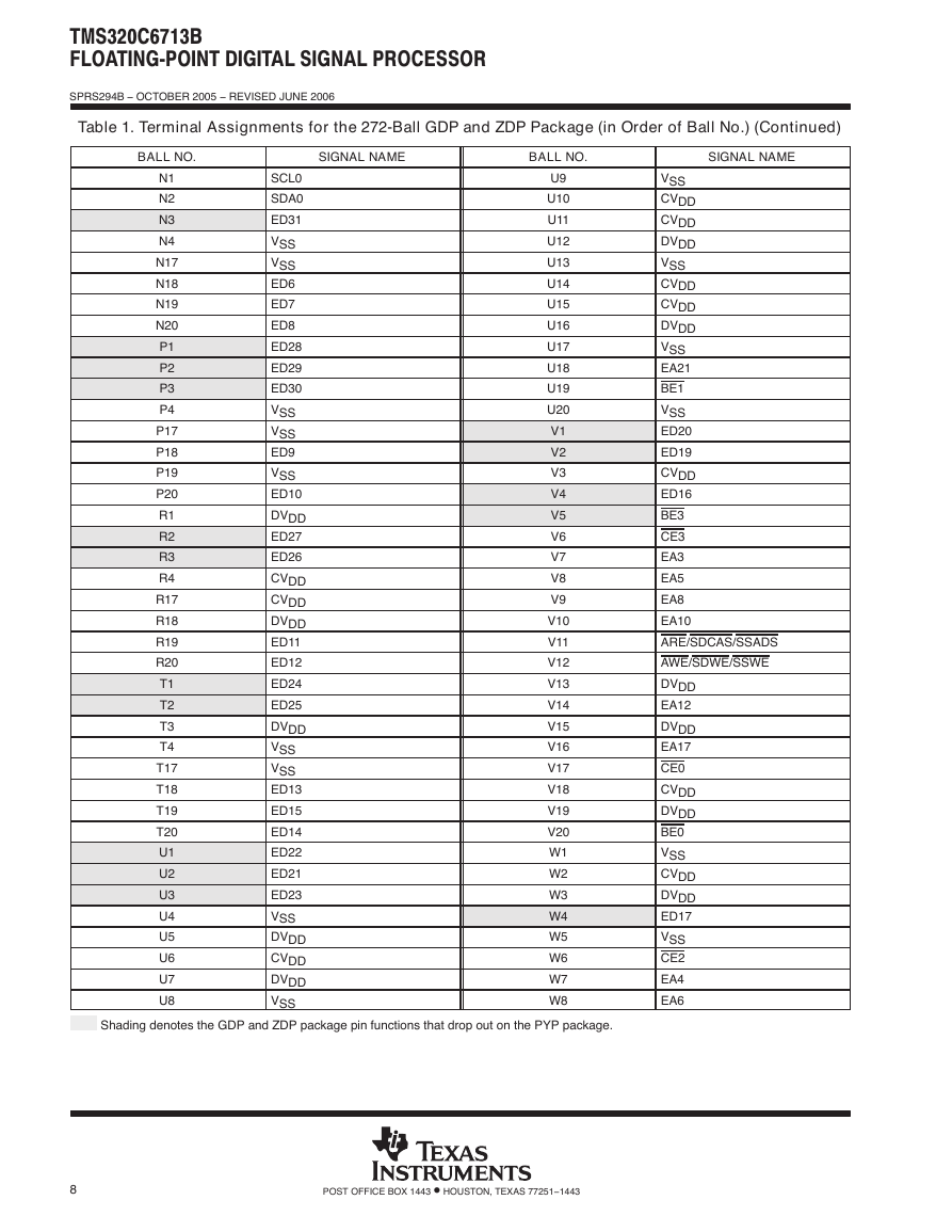
TMS320C6713B FLOATINGĆPOINT DIGITAL SIGNAL PROCESSOR SPRS294B − OCTOBER 2005 − REVISED JUNE 2006 Table 1. Terminal Assignments for the 272-Ball GDP and ZDP Package (in Order of Ball No.) (Continued) BALL NO. SIGNAL NAME BALL NO. SIGNAL NAME N1 N2 N3 N4 N17 N18 N19 N20 P1 P2 P3 P4 P17 P18 P19 P20 R1 R2 R3 R4 R17 R18 R19 R20 T1 T2 T3 T4 T17 T18 T19 T20 U1 U2 U3 U4 U5 U6 U7 U8 SCL0 SDA0 ED31 VSS VSS ED6 ED7 ED8 ED28 ED29 ED30 VSS VSS ED9 VSS ED10 DVDD ED27 ED26 CVDD CVDD DVDD ED11 ED12 ED24 ED25 DVDD VSS VSS ED13 ED15 ED14 ED22 ED21 ED23 VSS DVDD CVDD DVDD VSS U9 U10 U11 U12 U13 U14 U15 U16 U17 U18 U19 U20 V1 V2 V3 V4 V5 V6 V7 V8 V9 V10 V11 V12 V13 V14 V15 V16 V17 V18 V19 V20 W1 W2 W3 W4 W5 W6 W7 W8 VSS CVDD CVDD DVDD VSS CVDD CVDD DVDD VSS EA21 BE1 VSS ED20 ED19 CVDD ED16 BE3 CE3 EA3 EA5 EA8 EA10 ARE/SDCAS/SSADS AWE/SDWE/SSWE DVDD EA12 DVDD EA17 CE0 CVDD DVDD BE0 VSS CVDD DVDD ED17 VSS CE2 EA4 EA6 Shading denotes the GDP and ZDP package pin functions that drop out on the PYP package. 8 POST OFFICE BOX 1443 • HOUSTON, TEXAS 77251−1443
分享到:
收藏