1
�
Go register in the class website. I will close the self-registration after 2
weeks.
Website is in operation as of today.
2
�
The best way to find me is to send email to me or Fely Barrera to set up
an appointment. The phone is not very effective because I talk with
students in my office most of the time and I won’t pick up the phone when
I am talking to students.
The TA office hours are supposed to be accessible to most students. If
you have difficulty coming to the TA office hours, please let the TA or me
know and we can make arrangements.
3
�
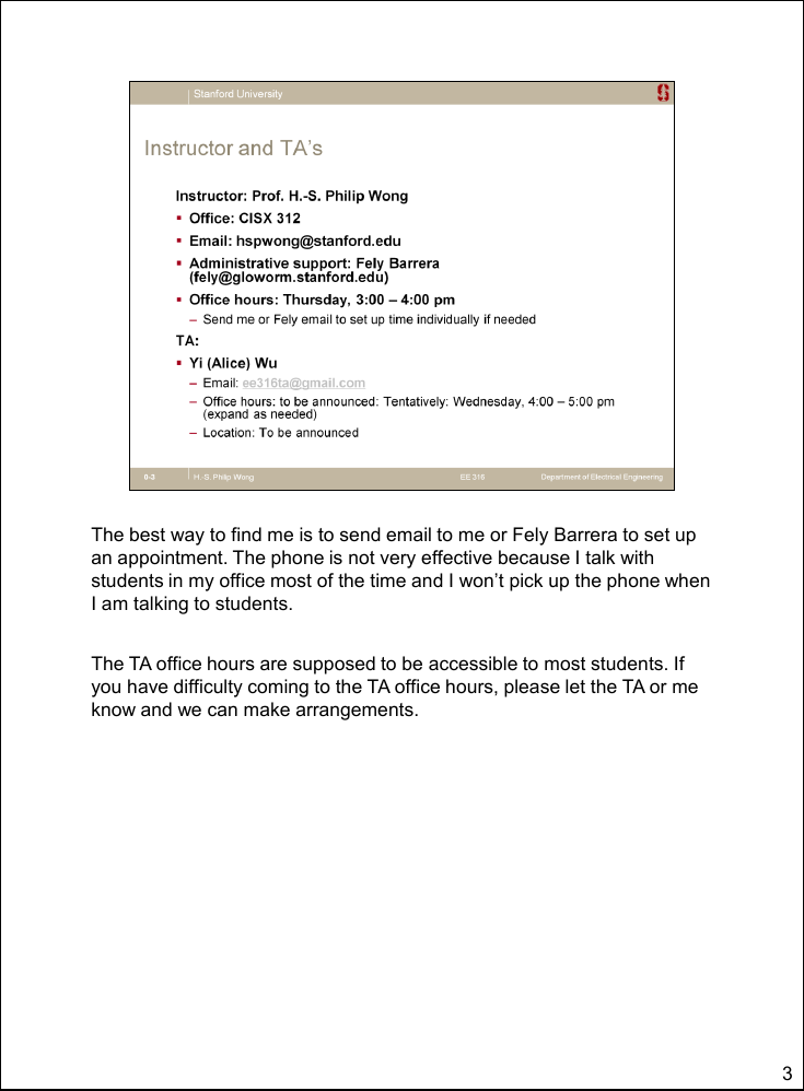
I work on device physics and device technology. Of the 16 years at IBM
Research, 13 years were on Si CMOS and 3 years were on
nanotechnology. I worked on image sensors, device modeling, double-
gate/multi-gate MOSFET, strained silicon, thin body SOI, Ge FET, carbon
nanotube FET, phase change memory, among other things. I managed
the team that explore technology options for future technology nodes. I
contributed to the chips that are in the Cell Processors in Xbox, Wii, and
PS2. At Stanford, my students continue to work on CMOS topics. Right
now, we are focusing on device performance estimation for future
technology nodes, modeling of parasitic capacitances, alternative
channel materials such as III-V compound semiconductor for the
transistor channel. For research on nanotechnology that aspires to
“replace” or complement Si CMOS, it is important to have a solid
understanding of what Si CMOS has to offer so there is a baseline for
comparison. Understanding the problems of Si CMOS is the “proving
ground” for novel technologies.
4
�
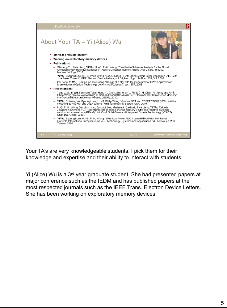
Your TA’s are very knowledgeable students. I pick them for their
knowledge and expertise and their ability to interact with students.
Yi (Alice) Wu is a 3rd year graduate student. She had presented papers at
major conference such as the IEDM and has published papers at the
most respected journals such as the IEEE Trans. Electron Device Letters.
She has been working on exploratory memory devices.
5
�
The course objectives are listed here. These are the kinds of things that
people expect you to know when you work as a device engineer in a
semiconductor company. These are also the skill you will find useful if
you are a circuit designer or a materials person because they help you
gain a better understanding of how device properties will affect circuit
performance (on the application side) and materials (in terms of what
material properties would be useful for devices). If you are a professor
who claims to know devices, then of course you should know the
materials in this class.
6
�
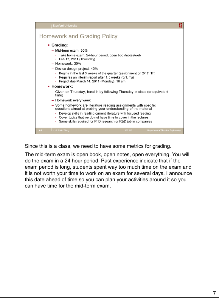
Since this is a class, we need to have some metrics for grading.
The mid-term exam is open book, open notes, open everything. You will
do the exam in a 24 hour period. Past experience indicate that if the
exam period is long, students spent way too much time on the exam and
it is not worth your time to work on an exam for several days. I announce
this date ahead of time so you can plan your activities around it so you
can have time for the mid-term exam.
7
�
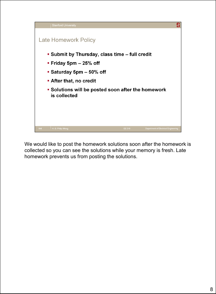
We would like to post the homework solutions soon after the homework is
collected so you can see the solutions while your memory is fresh. Late
homework prevents us from posting the solutions.
8
�



 2023年江西萍乡中考道德与法治真题及答案.doc
 2012年重庆南川中考生物真题及答案.doc
 2013年江西师范大学地理学综合及文艺理论基础考研真题.doc
 2020年四川甘孜小升初语文真题及答案I卷.doc
 2020年注册岩土工程师专业基础考试真题及答案.doc
 2023-2024学年福建省厦门市九年级上学期数学月考试题及答案.doc
 2021-2022学年辽宁省沈阳市大东区九年级上学期语文期末试题及答案.doc
 2022-2023学年北京东城区初三第一学期物理期末试卷及答案.doc
 2018上半年江西教师资格初中地理学科知识与教学能力真题及答案.doc
 2012年河北国家公务员申论考试真题及答案-省级.doc
 2020-2021学年江苏省扬州市江都区邵樊片九年级上学期数学第一次质量检测试题及答案.doc
 2022下半年黑龙江教师资格证中学综合素质真题及答案.doc