design
ideas
The best of
design ideas
8 Check it out at:
www.edn.com
Edited by Bill Travis
Steve Woodward, Chapel Hill, NC
Combine two 8-bit outputs to make one 16-bit DAC
Inexpensive, 16-bit, monolithic DACs
Combine two 8-bit outputs
to make one 16-bit DAC ..................................85
can serve almost all applications.
However, some applications require
unconventional approaches. This Design
Idea design concerns circuitry I recently
designed for a tunable-diode laser spec-
trometer for a Mars-exploration applica-
tion. The control circuitry included two
16-bit DACs that interface to the radia-
tion-hardened, 8051-variant 69RH051A
microcontroller. Because of the intend-
ed space-flight-qualified specification,
everything in the design had to consist
solely of components from the NPSL
(NASA parts-selection list). This restric-
tion posed a challenge, because, at design
finalization, the NPSL included no ap-
propriate, flight-qualified, 16-bit DACs,
and the budget included no funds for cer-
tification of new devices. I escaped from
this impasse by exploiting two fortuitous
facts: The update rate of the two DACs
was only tens of hertz, and the 69RH-
051A had a number of uncommitted, 8-
bit, 14.5-kHz PWM outputs. These out-
puts made one 16-bit DAC; a second pair
of PWM bits and an identical circuit
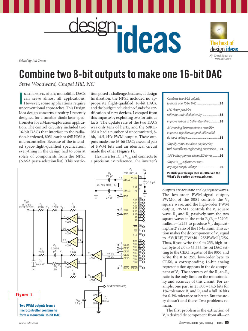
made the other (Figure 1).
Hex inverter IC1’s VCC rail connects to
a precision 5V reference. The inverter’s
LED driver provides
software-controlled intensity ..........................86
Improve roll-off of Sallen-Key filter ................88
AC-coupling instrumentation amplifier
improves rejection range of differential
dc input voltage..................................................88
Simplify computer-aided engineering
with scientific-to-engineering conversion ....94
1.5V battery powers white-LED driver ..........96
Simple VCOM adjustment uses
any logic-supply voltage ..................................96
Publish your Design Idea in EDN. See the
What’s Up section at www.edn.com.
outputs are accurate analog square waves.
The low-order PWM-signal output,
PWM0, of the 8051 controls the V3
square wave, and the high-order PWM
output, PWM1, controls the V1 square
wave. R2 and R6 passively sum the two
⫽3290/1
square waves in the ratio R2/R6
million⫽1/255 to produce V4, duplicat-
ing the 28 ratio of the 16-bit sum. This ac-
tion makes the dc component of V4 equal
to 5V(REF)(PWM0⫹255PWM1)/256.
Thus, if you write the 0 to 255, high-or-
der byte of a 0 to 65,535, 16-bit DAC set-
ting to the CEX1 register of the 8051 and
write the 0 to 255, low-order byte to
CEX0, a corresponding 16-bit analog
representation appears in the dc compo-
nent of V4. The accuracy of the R2-to-R6
ratio is the only limit on the monotonic-
ity and accuracy of this circuit. For ex-
ample, one part in 25,500⫽14.5 bits for
1%-tolerance R2 and R6 and a full 16 bits
for 0.3% tolerance or better. But the sto-
ry doesn’t end there. Two problems re-
main.
The first problem is the extraction of
V4’s desired dc component from all—or
September 30, 2004 | edn 85
VDAC
0 TO 5V
(REFERENCE)
R3
200k
V4
R2
3.92k
V1
R1
1M
3
IC1
4
HC04
10
HC04
11
IC1
12
HC04
13
IC1
V2
R4
3.92k
2
HC04
1
IC1
PWM1
PWM0
0.0056
C8
F
V3
R6
1M
9
IC1
8
HC04
R7
1M
R5
200k
C9
0.01 F
IC2
69RH051 A
5V
18
XTAL1
VDD2
C4
27 pF
14.756 MHz
Y1
19
9
XTAL2
RST
C5
27 pF
0.1 F
40
20
31
28
27
26
25
24
23
22
21
16
17
30
32
33
34
35
36
37
38
39
29
VSS
EA
A15
A14
A13
A12
A11
A10
A9
A8
WR
R0
ALE
AD7
AD6
AD5
AD4
AD3
AD2
AD1
AD0
11
10
TX0
RX0
8
7
6
5
4
CEX4
CEX3
CEX2
CEX1
CEX0
12
INTO PSEN
5
IC1
6
HC04
5V (REFERENCE)
Figure 1
Two PWM outputs from a
microcontroller combine to
form a monotonic 16-bit DAC.
www.edn.com
C1B
0.1 F
14
VCC
GND
7
IC1
HCO4
�
design
ideas
at least 15 or 16 bits⫽99.995%—of the
undesired square-wave ac ripple. The R3-
C9 lowpass filter does some of this work.
If you make C9 large enough, in princi-
ple, the filter could do the whole job. The
reason this simple approach wouldn’t
work is that, to get such a large ripple at-
tenuation of approximately 90 dB with a
single-stage RC filter would require an
approximately 300-msec time constant
and a resultant 3-sec, 16-bit settling time.
This glacial response time would be too
slow even for this undemanding applica-
tion. To speed things, the R4, R5, R7, C8
network synthesizes and then sums V2: an
inverse-polarity duplicate of V4’s 14.5-
kHz ac component. This summation ac-
tively nulls out approximately 99% of the
ripple. This nullifying action leaves such
a small residue that an approximately 2-
msec and, therefore, approximately 25-
msec-settling-time R3C9 product easily
erases it.
The other problem is compensation for
the low, but still nonzero, on-resistance of
the HC14 internal CMOS switches, so
that the resistance doesn’t perturb the
critical R2-to-R6 ratio. This issue is of no
particular concern for R6, because the R6-
to-on-resistance ratio is greater than
10,000-to-1, making any associated error
negligible. This situation is not the case
for R2, however, in which, despite the
triple-parallel gates, the R2-to-on-resist-
ance ratio is approximately 300-to-1,
which is small enough to merit attention.
Load-cancellation resistor R1 provides
such attention. R1 sums a current into the
R2 driving node that, because it is equal in
magnitude but opposite in phase to the
current through R6, effectively cancels the
load on the R2 drivers. This process makes
the combined on-resistance approxi-
mately 100 times less important than it
otherwise would be. The result is a sim-
ple, highly linear and accurate voltage-
output DAC with a respectable, if not
blazingly fast, settling time of approxi-
mately 25 msec. And the most important
result, in this case, was a parts list with an
impeccable NPSL-compliant pedigree.왏
Neda Shahi and Bjorn Starmark, Maxim Integrated Products, Sunnyvale, CA
LED driver provides software-controlled intensity
Recent advances in
CMSH1-100
D1 SMB
R1
51
VIN
C1
L1
1
2
22 H
ELL6RH
3.3 F
1206
10V
11
VIN
GATE
10
12
1
2
3
4
5
6
7
8
9
CA⫹
CS⫺
IC1
CS
SCLK
DIN
CL
DACOUT
FB
COMP
GND
MAX1932
12QFN
Q1
IRLL110
SOT223
R6
12k
C5
0.33 F
R2
16k
C3
0.1 F
1206
100V
C2
0.47 F
1210
100V
VIN
R3
56k
Q2
MMBT5551
SOT23
Q3
MMBT3906
SOT23
R4
10k
R5
510k
R7
10k
LED1
LED2
LED(N-1)
LED(N)
C4
0.1 F
CONTROLLER
TO
VCC
GND
operating efficiency
have expanded the use
of LEDs from one of mere
indicators
to becoming
driving forces in electronic
lighting. Increased reliabili-
ty and ruggedness (versus
other lighting technologies)
gives the LED a bright fu-
ture indeed. Vendors in re-
cent years have introduced
many ICs for driving LEDs,
but the problem of driving
serial chains of LEDs has re-
ceived less attention. One
approach to that problem
adapts a bias-supply IC
for APDs (avalanche
photodiodes) to provide
adjustable-current,
soft-
ware shutdown, and logic
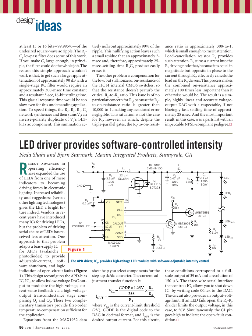
indication of open-circuit faults (Figure
1). This design reconfigures the APD-bias
IC, IC1, to allow its low-voltage DAC out-
put to modulate the high-voltage, cur-
rent-sense feedback via a high-voltage-
output transconductance stage com-
prising Q2 and Q3. These two comple-
mentary transistors provide first-order
temperature-compensation sufficient for
the application.
Figure 1
Equations from the MAX1932 data
86 edn | September 30, 2004
The APD driver, IC1, provides high-voltage LED modules with software-adjustable intensity control.
sheet help you select components for the
step-up dc/dc converter. The current-ad-
justment transfer function is:
where VCL is the current-limit threshold
(2V), CODE is the digital code to the
DAC in decimal format, and IOUT is the
desired output current. For this circuit,
these conditions correspond to a full-
scale output of 39 mA and a resolution of
150 A. The three-wire serial interface
that controls IC1 allows you to shut down
IC1 by writing code 00hex to the DAC.
The circuit also provides an output-volt-
age limit. If an LED fails open, the R5-R7
divider limits the output voltage, in this
case, to 50V. Simultaneously, the CL pin
goes high to indicate the open-fault con-
dition.왏
www.edn.com
�
design
ideas
Doug Glenn, Teledyne, Lewisburg, TN
Improve roll-off of Sallen-Key filter
The well-documented Sallen-
–10
10
0
–20
–30
–40
–50
–60
Key active filter is a staple of
analog design. This Design Idea
shows a way to obtain better roll-off
by adding just a few common pas-
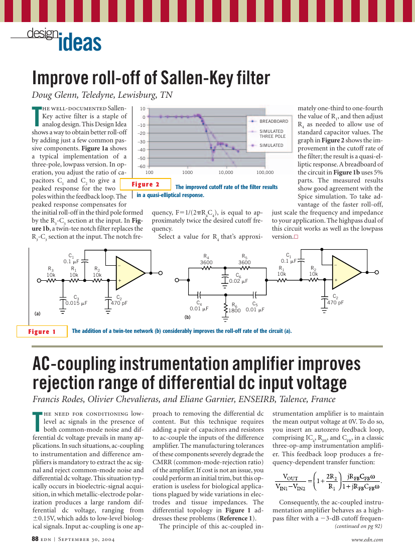
sive components. Figure 1a shows
a typical implementation of a
three-pole, lowpass version. In op-
eration, you adjust the ratio of ca-
pacitors C1 and C2 to give a
peaked response for the two
poles within the feedback loop. The
peaked response compensates for
the initial roll-off in the third pole formed
by the R3-C3 section at the input. In Fig-
ure 1b, a twin-tee notch filter replaces the
R3-C3 section at the input. The notch fre-
100
1000
10,000
100,000
Figure 2
The improved cutoff rate of the filter results
in a quasi-elliptical response.
quency, F⫽1/(2R4C4), is equal to ap-
proximately twice the desired cutoff fre-
quency.
Select a value for R4 that’s approxi-
BREADBOARD
SIMULATED
THREE POLE
SIMULATED
mately one-third to one-fourth
the value of R1, and then adjust
R4 as needed to allow use of
standard capacitor values. The
graph in Figure 2 shows the im-
provement in the cutoff rate of
the filter; the result is a quasi-el-
liptic response. A breadboard of
the circuit in Figure 1b uses 5%
parts. The measured results
show good agreement with the
Spice simulation. To take ad-
vantage of the faster roll-off,
just scale the frequency and impedance
to your application. The highpass dual of
this circuit works as well as the lowpass
version.왏
C1
0.1 F
R1
10k
R3
10k
R2
10k
_
+
C3
0.015 F
C2
470 pF
(a)
R4
3600
R5
3600
C6
0.02 F
C1
0.1 F
R1
10k
R2
10k
C4
0.01 F
(b)
R6
1800
C5
0.01 F
_
+
C2
470 pF
Figure 1
The addition of a twin-tee network (b) considerably improves the roll-off rate of the circuit (a).
AC-coupling instrumentation amplifier improves
rejection range of differential dc input voltage
The need for conditioning low-
Francis Rodes, Olivier Chevalieras, and Eliane Garnier, ENSEIRB, Talence, France
level ac signals in the presence of
both common-mode noise and dif-
ferential dc voltage prevails in many ap-
plications. In such situations, ac-coupling
to instrumentation and difference am-
plifiers is mandatory to extract the ac sig-
nal and reject common-mode noise and
differential dc voltage. This situation typ-
ically occurs in bioelectric-signal acqui-
sition, in which metallic-electrode polar-
ization produces a large random dif-
ferential dc voltage,
from
⫾0.15V, which adds to low-level biolog-
ical signals. Input ac-coupling is one ap-
88 edn | September 30, 2004
ranging
proach to removing the differential dc
content. But this technique requires
adding a pair of capacitors and resistors
to ac-couple the inputs of the difference
amplifier. The manufacturing tolerances
of these components severely degrade the
CMRR (common-mode-rejection ratio)
of the amplifier. If cost is not an issue, you
could perform an initial trim, but this op-
eration is useless for biological applica-
tions plagued by wide variations in elec-
trodes and tissue impedances. The
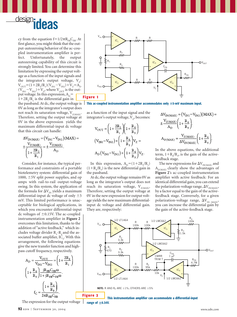
differential topology in Figure 1 ad-
dresses these problems (Reference 1).
The principle of this ac-coupled in-
strumentation amplifier is to maintain
the mean output voltage at 0V. To do so,
you insert an autozero feedback loop,
comprising IC4, RFB, and CFB, in a classic
three-op-amp instrumentation amplifi-
er. This feedback loop produces a fre-
quency-dependent transfer function:
Consequently, the ac-coupled instru-
mentation amplifier behaves as a high-
pass filter with a ⫺3-dB cutoff frequen-
(continued on pg 92)
www.edn.com
�
design
ideas
the
cy from the equation f⫽1/2RFBCFB. At
first glance, you might think that the out-
put-autozeroing behavior of the ac-cou-
pled instrumentation amplifier is per-
fect. Unfortunately,
output
autozeroing capability of this circuit is
strongly limited. You can determine this
limitation by expressing the output volt-
age as a function of the input signals and
the integrator’s output voltage, VZ:
⫽(1⫹2R2/R1)(VIN1
⫽AD
VOUT
⫺VIN2)⫹VZ, where VOUT is the out-
(VIN1
⫽
put voltage. In this expression, AD
1⫹2R2/R1 is the differential gain in
the passband. At dc, the output voltage is
0V as long as the integrator’s output does
not reach its saturation voltage, VZ(MAX).
Therefore, setting the output voltage at
0V in the above expression yields the
maximum differential-input dc voltage
that this circuit can handle:
⫺VIN2)⫹VZ
VIN1
+
_
IC1
R2
R2
R1
_
+
IC2
VIN2
R
R
R
_
+
R
IC3
VZ
VOUT
CFB
RFB
_
+
IC4
Figure 1
This ac-coupled instrumentation amplifier accommodates only ⫾⫾5-mV maximum input.
as a function of the input signal and the
integrator’s output voltage, VZ, becomes:
Consider, for instance, the typical per-
formance and constraints of a portable
biotelemetry system: differential gain of
1000, ⫾5V split power supplies, and op
amps with rail-to-rail output-voltage
swing. In this system, the application of
the formula for ⌬VIN yields a maximum
differential-input dc voltage of only ⫾5
mV. This limited performance is unac-
ceptable for biological applications, in
which you encounter differential-input
dc voltages of ⫾0.15V. The ac-coupled
instrumentation amplifier in Figure 2
overcomes this limitation, thanks to the
addition of “active feedback,” which in-
cludes voltage divider R3-R4 and the as-
sociated buffer amplifier, IC5. With this
arrangement, the following equations
give the new transfer function and high-
pass cutoff frequency, respectively.
In this expression, AD
⫽(1⫹2R2/R1)
(1⫹R4/R3) is the new differential gain in
the passband.
At dc, the output voltage remains 0V as
long as the integrator’s output does not
reach its saturation voltage, VZ(MAX).
Therefore, setting the output voltage at
0V in the new expression for output volt-
age yields the new maximum differential-
input dc voltage and differential gain.
They are, respectively:
In the above equations, the additional
term, 1⫹R4/R3, is the gain of the active-
feedback stage.
The new expressions for ⌬VIN(MAX) and
AD(MAX) clearly show the advantages of
Figure 2’s ac-coupled instrumentation
amplifier with active feedback: For an
identical differential gain, you can extend
the polarization-voltage range, ⌬VIN(MAX),
by a factor equal to the gain of the active-
feedback stage. Conversely, for a given
polarization-voltage range, ⌬VIN (MAX),
you can increase the differential gain by
the gain of the active-feedback stage.
VIN1
1/2 LT1464
+
_
IC1
R
100k
R
100k
1/2 LMC662
IC5
+
_
R4
100k
R3
1.5k
R2
3.3k
R2
3.3k
R1
470
_
+
1/2 LMC662
IC3
CMRR
TRIM T
CFB
1 F
_
+
IC2
1/2 LT1464
VIN2
R
100k
RF
95k
_
+
IC4
1/2 LMC662
10k
VZ
VOUT
RFB
4.7M
The expression for the output voltage
92 edn | September 30, 2004
NOTE: R AND RF ARE ⫾1%; OTHERS ARE ⫾5%
Figure 2
This instrumentation amplifier can accommodate a differential-input
range of ⫾⫾0.34V.
www.edn.com
�
design
ideas
The only drawback of this topology is
apparent in the expression for fC, the
highpass cutoff frequency.You multiply
this frequency by the gain of the active-
feedback stage. Therefore, to maintain a
given cutoff frequency, you must multi-
ply the time constant by a factor equal to
the active-feedback stage gain. This fac-
tor can be an issue in processing signals
whose spectrum includes low-frequency
components. In such applications, RFB
and CFB can reach prohibitive values.
Consequently, you must make a trade-off
between the time constant and the active-
feedback stage gain. The component val-
ues in Figure 2 are a typical example of
such a trade-off: The values are for an
EEG (electroencephalogram) amplifier
with ⫾5V split power supplies. The am-
plifier has a differential gain of 1000 and
a highpass cutoff frequency of 2.3 Hz,
and it can handle a differential-input dc-
voltage range of ⫾0.34V.
To obtain this performance, you set the
active-feedback stage gain and the differ-
ential-amplifier gain, respectively, to 67.6
and 15. With these gain values, the noise
performance of the ac-coupled instru-
mentation amplifier of Figure 2 is simi-
lar to that of a classic instrumentation
amplifier. This situation occurs because
the autozeroing and active-feedback
stages, IC4 and IC5, are after the input dif-
ferential stage, IC1 and IC2. Consequent-
ly, the gain of the differential stage rough-
ly divides their respective noise con-
tributions, which are therefore negligible.
You can use several low-noise op-amps
for IC1 and IC2. For portable bioteleme-
try applications, the LT1464 is a good
compromise for input-noise density,
noise-corner frequency, input-bias cur-
rent and current drain. (Respectively:
⫽0.4
VNOISE
pA, and ICC
⫽26 nV/公Hz, fC
⫽230 A.)
⫽9 Hz, IBIAS
A theoretical analysis using the LT
1464’s noise parameters shows that un-
der worst-case conditions, the input-
noise voltage should not exceed 11 V
rms. Tests on prototypes confirm this
prediction; the tests effectively measure
input-noise voltages of 3 to 6 V rms. To
sum up, an ac-coupled instrumentation
amplifier with active feedback is well-
suited for applications requiring high dif-
ferential gain, a capability for handling
large differential-input dc voltages, and
low-noise performance.왏
Reference
1. Stitt, Mark, “AC-Coupled Instru-
mentation and Difference Amplifier,”
Burr-Brown, AB-008, May 1990.
Simplify computer-aided engineering
with scientific-to-engineering conversion
The simple yet useful
Alexander Bell, Infosoft International, Rego Park, NY
formula in this Design
Idea enables conver-
sion from scientific format
(for example, 2.2⫺9), which
is typical for CAE (com-
puter-aided-engineering),
double-precision output
values,
“human-
friendly” engineering for-
mat (for example, 2.2 nF).
The engineering format is
more suitable for bills of
material and other electri-
cal and electronic-engi-
neering
and specifications.
documents
into
The formula is in VB; you
could use it in any VB/VBA-
backed software applications.
In this example, the function
is in a code module of an MS
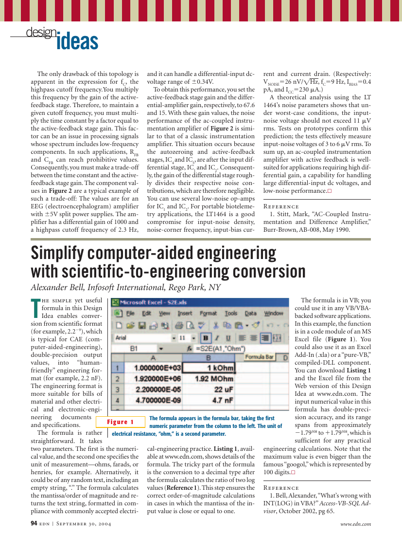
Excel file (Figure 1). You
could also use it as an Excel
Add-In (.xla) or a “pure-VB,”
compiled-DLL component.
You can download Listing 1
and the Excel file from the
Web version of this Design
Idea at www.edn.com. The
input numerical value in this
formula has double-preci-
sion accuracy, and its range
spans from approximately
⫺1.79308 to ⫹1.79308, which is
sufficient for any practical
engineering calculations. Note that the
maximum value is even bigger than the
famous “googol,” which is represented by
100 digits.왏
Reference
1. Bell, Alexander, “What’s wrong with
INT(LOG) in VBA?” Access-VB-SQL Ad-
visor, October 2002, pg 65.
www.edn.com
Figure 1
The formula appears in the formula bar, taking the first
numeric parameter from the column to the left. The unit of
electrical resistance, “ohm,” is a second parameter.
The formula is rather
It takes
straightforward.
two parameters. The first is the numeri-
cal value, and the second one specifies the
unit of measurement—ohms, farads, or
henries, for example. Alternatively, it
could be of any random text, including an
empty string, “.” The formula calculates
the mantissa/order of magnitude and re-
turns the text string, formatted in com-
pliance with commonly accepted electri-
94 edn | September 30, 2004
cal-engineering practice. Listing 1, avail-
able at www.edn.com, shows details of the
formula. The tricky part of the formula
is the conversion to a decimal type after
the formula calculates the ratio of two log
values (Reference 1). This step ensures the
correct order-of-magnitude calculations
in cases in which the mantissa of the in-
put value is close or equal to one.
�
design
ideas
Steve Caldwell, Maxim Integrated Products, Chandler, AZ
1.5V battery powers white-LED driver
Although white LEDs are common
10 H
L1
+
1.5V
C1
10 F
in a variety of lighting applications,
their 3 to 4V forward-voltage drop
makes low-voltage applications challeng-
ing. Charge pumps and other ICs are
available for driving white LEDs, but they
generally don’t work with the low supply
voltage of 1.5V in single-cell-battery ap-
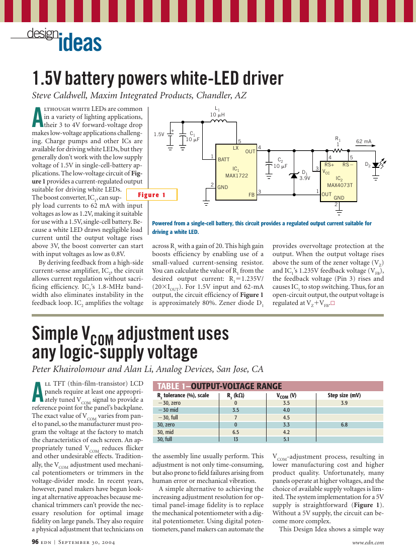
plications. The low-voltage circuit of Fig-
ure 1 provides a current-regulated output
suitable for driving white LEDs.
The boost converter, IC1, can sup-
ply load currents to 62 mA with input
voltages as low as 1.2V, making it suitable
for use with a 1.5V, single-cell battery. Be-
cause a white LED draws negligible load
current until the output voltage rises
above 3V, the boost converter can start
with input voltages as low as 0.8V.
By deriving feedback from a high-side
current-sense amplifier, IC2, the circuit
allows current regulation without sacri-
ficing efficiency. IC2’s 1.8-MHz band-
width also eliminates instability in the
feedback loop. IC2 amplifies the voltage
Figure 1
5
LX
4
OUT
1
BATT
IC1
MAX1722
2
GND
3
FB
C2
10 F
D1
3.9V
3
1
R1
1
62 mA
5
RSⳮ
D2
4
RS+
VCC
IC2
MAX4073T
OUT
GND
2
Powered from a single-cell battery, this circuit provides a regulated output current suitable for
driving a white LED.
across R1 with a gain of 20. This high gain
boosts efficiency by enabling use of a
small-valued current-sensing resistor.
You can calculate the value of R1 from the
⫽1.235V/
desired output current: R1
(20⫻IOUT). For 1.5V input and 62-mA
output, the circuit efficiency of Figure 1
is approximately 80%. Zener diode D1
provides overvoltage protection at the
output. When the output voltage rises
above the sum of the zener voltage (VZ)
and IC1’s 1.235V feedback voltage (VFB),
the feedback voltage (Pin 3) rises and
causes IC1 to stop switching. Thus, for an
open-circuit output, the output voltage is
regulated at VZ
⫹VFB.왏
Simple VCOM adjustment uses
any logic-supply voltage
All TFT (thin-film-transistor) LCD
Peter Khairolomour and Alan Li, Analog Devices, San Jose, CA
panels require at least one appropri-
ately tuned VCOM signal to provide a
reference point for the panel’s backplane.
The exact value of VCOM varies from pan-
el to panel, so the manufacturer must pro-
gram the voltage at the factory to match
the characteristics of each screen. An ap-
propriately tuned VCOM reduces flicker
and other undesirable effects. Tradition-
ally, the VCOM adjustment used mechani-
cal potentiometers or trimmers in the
voltage-divider mode. In recent years,
however, panel makers have begun look-
ing at alternative approaches because me-
chanical trimmers can’t provide the nec-
essary resolution for optimal image
fidelity on large panels. They also require
a physical adjustment that technicians on
96 edn | September 30, 2004
R2 (k⍀⍀)
TABLE 1—OUTPUT-VOLTAGE RANGE
R2 tolerance (%), scale
ⳮ30, zero
ⳮ30 mid
ⳮ30, full
30, zero
30, mid
30, full
0
3.5
7
0
6.5
13
3.5
4.0
4.5
3.3
4.2
5.1
VCOM (V)
Step size (mV)
3.9
6.8
the assembly line usually perform. This
adjustment is not only time-consuming,
but also prone to field failures arising from
human error or mechanical vibration.
A simple alternative to achieving the
increasing adjustment resolution for op-
timal panel-image fidelity is to replace
the mechanical potentiometer with a dig-
ital potentiometer. Using digital poten-
tiometers, panel makers can automate the
VCOM-adjustment process, resulting in
lower manufacturing cost and higher
product quality. Unfortunately, many
panels operate at higher voltages, and the
choice of available supply voltages is lim-
ited. The system implementation for a 5V
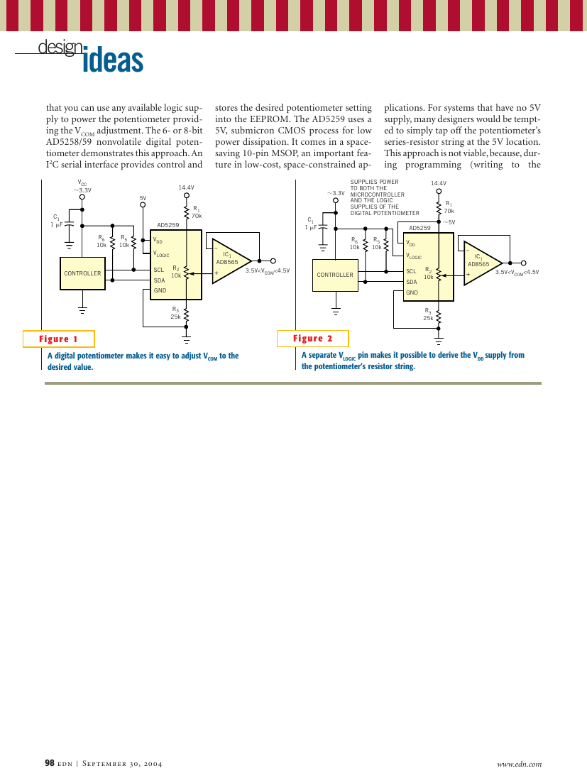
supply is straightforward (Figure 1).
Without a 5V supply, the circuit can be-
come more complex.
This Design Idea shows a simple way
www.edn.com
�
design
ideas
that you can use any available logic sup-
ply to power the potentiometer provid-
ing the VCOM adjustment. The 6- or 8-bit
AD5258/59 nonvolatile digital poten-
tiometer demonstrates this approach. An
I2C serial interface provides control and
stores the desired potentiometer setting
into the EEPROM. The AD5259 uses a
5V, submicron CMOS process for low
power dissipation. It comes in a space-
saving 10-pin MSOP, an important fea-
ture in low-cost, space-constrained ap-
plications. For systems that have no 5V
supply, many designers would be tempt-
ed to simply tap off the potentiometer’s
series-resistor string at the 5V location.
This approach is not viable, because, dur-
the
ing programming (writing
to
VCC
⬃3.3V
C1
1 F
R6
10k
R5
10k
CONTROLLER
5V
14.4V
R1
70k
AD5259
VDD
VLOGIC
SCL
SDA
GND
R2
10k
R3
25k
⬃3.3V
SUPPLIES POWER
TO BOTH THE
MICROCONTROLLER
AND THE LOGIC
SUPPLIES OF THE
DIGITAL POTENTIOMETER
AD5259
14.4V
R1
70k
⬃5V
C1
1 F
_
IC1
AD8565
+
R6
10k
R5
10k
3.5V
design
ideas
EEPROM), the AD5259’s VLOGIC pin typ-
ically draws 35 mA. It cannot draw this
current level through R1 because the volt-
age drop would be too large. For this rea-
son, the AD5259 has a separate VLOGIC pin
that can connect to any available logic
supply. In Figure 2, VLOGIC uses the sup-
ply voltage from the microcontroller that
is controlling the digital potentiometer.
Now, VLOGIC draws the 35-mA program-
ming current, and VDD draws only mi-
croamps of supply current to bias the in-
ternal switches in the digital potentio-
meter’s internal resistor string. If the pan-
el requires a higher VCOM voltage, you can
add two resistors to place the op amp in
a noninverting gain configuration.
The digital potentiometer has ⫾30%
end-to-end resistance tolerance. Assum-
ing that the tolerances of R1, R3, and VDD
are negligible compared with those of the
potentiometer, you can achieve the range
of output values that Table 1 shows. As-
sume that the desired value of VCOM is
VDD
VLOGIC
DGND
SCL
SDA
AD0
AD1
RDAC EEPROM
RDAC1
REGISTER
RDAC1
A1
W1
B1
DATA
8
8
CONTROL
COMMAND-DECODE LOGIC
ADDRESS-DECODE LOGIC
CONTROL LOGIC
I2C
SERIAL
INTERFACE
POWER-
ON
RESET
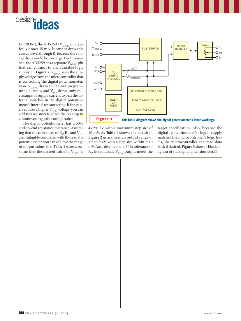
Figure 3
This block diagram shows the digital potentiometer’s inner workings.
4V⫾0.5V, with a maximum step size of
10 mV. As Table 1 shows, the circuit in
Figure 2 guarantees an output range of
3.5 to 5.4V with a step size within ⫾10
mV. And, despite the ⫾30% tolerance of
R2, the midscale VCOM output meets the
target specification. Also, because the
digital potentiometer’s
logic supply
matches the microcontroller’s logic lev-
els, the microcontroller can read data
back if desired. Figure 3 shows a block di-
agram of the digital potentiometer.왏
100 edn | September 30, 2004
www.edn.com
�


 2023年江西萍乡中考道德与法治真题及答案.doc
 2012年重庆南川中考生物真题及答案.doc
 2013年江西师范大学地理学综合及文艺理论基础考研真题.doc
 2020年四川甘孜小升初语文真题及答案I卷.doc
 2020年注册岩土工程师专业基础考试真题及答案.doc
 2023-2024学年福建省厦门市九年级上学期数学月考试题及答案.doc
 2021-2022学年辽宁省沈阳市大东区九年级上学期语文期末试题及答案.doc
 2022-2023学年北京东城区初三第一学期物理期末试卷及答案.doc
 2018上半年江西教师资格初中地理学科知识与教学能力真题及答案.doc
 2012年河北国家公务员申论考试真题及答案-省级.doc
 2020-2021学年江苏省扬州市江都区邵樊片九年级上学期数学第一次质量检测试题及答案.doc
 2022下半年黑龙江教师资格证中学综合素质真题及答案.doc