Introduction to Digital Design
Using Digilent FPGA Boards
─ Block Diagram / Verilog Examples
Richard E. Haskell
Darrin M. Hanna
Oakland University, Rochester, Michigan
LBE Books
Rochester Hills, MI
�
Copyright 2009 by LBE Books, LLC. All rights reserved.
ISBN 978-0-9801337-9-0
Online Version
Published by LBE Books, LLC
1202 Walton Boulevard
Suite 214
Rochester Hills, MI 48307
www.lbebooks.com
ii
�
Preface
A major revolution in digital design has taken place over the past decade.
Field programmable gate arrays (FPGAs) can now contain over a million equivalent
logic gates and tens of thousands of flip-flops. This means that it is not possible to
use traditional methods of logic design involving the drawing of logic diagrams
when the digital circuit may contain thousands of gates. The reality is that today
digital systems are designed by writing software in the form of hardware
description languages (HDLs). The most common HDLs used today are VHDL and
Verilog. Both are in widespread use. When using these hardware description
languages the designer typically describes the behavior of the logic circuit rather
than writing traditional Boolean logic equations. Computer-aided design tools are
used to both simulate the Verilog or VHDL design and to synthesize the design to
actual hardware.
This book assumes no previous knowledge of digital design. We use 30
examples to show you how to get started designing digital circuits that you can
implement on a Xilinx Spartan3E FPGA using either the Digilent BASYS™ system
board that can be purchased from www.digilentinc.com for $59 or the Digilent
Nexys-2 board that costs $99. We will use Active-HDL from Aldec to design,
simulate, synthesize, and implement our digital designs. A free student edition of
Active-HDL is available from Aldec, Inc. (www.aldec.com). To synthesize your
designs to a Spartan3E FPGA you will need to download the free ISE WebPACK
from Xilinx, Inc. (www.xilinx.com). The Xilinx synthesis tools are called from
within the Aldec Active-HDL integrated GUI. We will use the ExPort utility to
download your synthesized design to the Spartan3E FPGA. ExPort is part of the
Adept software suite
that you can download free from Digilent, Inc.
(www.digilentinc.com). A more complete book called Digital Design Using
Digilent FPGA Boards – Verilog / Active-HDL Edition is also available from
Digilent or LBE Books (www.lbebooks.com). This more comprehensive book
contains over 75 examples including examples of using the VGA and PS/2 ports.
Similar books that use VHDL are also available from Digilent or LBE Books.
Many colleagues and students have influenced the development of this
book. Their stimulating discussions, probing questions, and critical comments are
greatly appreciated.
Richard E. Haskell
Darrin M. Hanna
iii
�
Introduction to Digital Design
Using Digilent FPGA Boards
─ Block Diagram / Verilog Examples
Table of Contents
1
6
11
15
20
22
25
30
37
42
47
55
60
65
68
70
Introduction – Digital Design Using FPGAs
Example 1 – Switches and LEDs
Example 2 – 2-Input Gates
Example 3 – Multiple-Input Gates
Example 4 – Equality Detector
Example 5 – 2-to-1 Multiplexer
Example 6 – Quad 2-to-1 Multiplexer
Example 7 – 4-to-1 Multiplexer
Example 8 – Clocks and Counters
Example 9 – 7-Segment Decoder
Example 10 – 7-Segment Displays: x7seg and x7segb
Example 11 – 2's Complement 4-Bit Saturator
Example 12 – Full Adder
Example 13 – 4-Bit Adder
Example 14 – N-Bit Adder
Example 15 – N-Bit Comparator
Available only in print vesion
Example 16 – Edge-Triggered D Flip-Flop
Example 17 – D Flip-Flops in Verilog
Example 18 – Divide-by-2 Counter
Example 19 – Registers
Example 20 – N-Bit Register in Verilog
Example 21 – Shift Registers
Example 22 – Ring Counters
Example 23 – Johnson Counters
Example 24 – Debounce Pushbuttons
Example 25 – Clock Pulse
Example 26 – Arbitrary Waveform
Example 27 – Pulse-Width Modulation (PWM)
Example 28 – Controlling Position of a Servo
Example 29 – Scrolling the 7-Segment Display
Example 30 – Fibonacci Sequence
iv
�
Appendix A – Aldec Active-HDL Tutorial
Part 1: Project Setup
Part 2: Design Entry – sw2led.bde
Part 3: Synthesis and Implementation
Part 4: Program FPGA Board
Part 5: Design Entry – gates2.bde
Part 6: Simulation
Part 7: Design Entry – HDE
Part 8: Simulation – gates2
Appendix B – Number Systems
B.1 Counting in Binary and Hexadecimal
B.2 Positional Notation
B.3 Fractional Numbers
B.4 Number System Conversions
B.5 Negative Numbers
109
109
113
116
120
122
128
132
135
Available only in print vesion
Appendix C – Basic Logic Gates
C.1 Truth Tables and Logic Equations
C.2 Positive and Negative Logic: De Morgan’s Theorem
C.3 Sum of Products Design
C.4 Product of Sums Design
Appendix D – Boolean Algebra and Logic Equations
D.1 Boolean Theorems
D.2 Karnaugh Maps
Appendix E – Verilog Quick Reference Guide
175
v
�
�
Introduction
1
Introduction
Digital Design Using FPGAs
The first integrated circuits that were developed in the early 1960s contained less
that 100 transistors on a chip and are called small-scale integrated (SSI) circuits.
Medium-scale integrated (MSI) circuits, developed in the late 1960s, contain up to
several hundreds of transistors on a chip. By the mid 1970s large-scale integrated (LSI)
circuits containing several thousands of transistors had been developed. Very-large-scale
integrated (VLSI) circuits containing over 100,000 transistors had been developed by the
early 1980s. This trend has continued to the present day with 1,000,000 transistors on a
chip by the late 1980s, 10,000,000 transistors on a chip by the mid-1990s, over
100,000,000 transistors by 2004, and up to 1,000,000,000 transistors on a chip today.
This exponential growth in the amount of digital logic that can be packed into a single
chip has produced serious problems for the digital designer. How can an engineer, or
even a team of engineers, design a digital logic circuit that will end up containing
millions of transistors?
In Appendix C we show that any digital logic circuit can be made from only three
types of basic gates: AND, OR, and NOT. In fact, we will see that any digital logic
circuit can be made using only NAND gates (or only NOR gates), where each NAND or
NOR gate contains four transistors. These basic gates were provided in SSI chips using
various technologies, the most popular being transistor-transistor logic (TTL). These
TTL chips were the mainstay of digital design throughout the 1960s and 1970s. Many
MSI TTL chips became available for performing all types of digital logic functions such
as decoders, adders, multiplexers, comparators, and many others.
By the 1980s thousands of gates could fit on a single chip. Thus, several different
varieties of programmable logic devices (PLDs) were developed in which arrays
containing large numbers of AND, OR, and NOT gates were arranged in a single chip
without any predetermined function. Rather, the designer could design any type of
digital circuit and implement it by connecting the internal gates in a particular way. This
is usually done by opening up fuse links within the chip using computer-aided tools.
Eventually the equivalent of many PLDs on a single chip led to complex programmable
logic devices (CPLDs).
Field Programmable Gate Arrays (FPGAs)
A completely different architecture was introduced in the mid-1980’s that uses
RAM-based lookup tables instead of AND-OR gates to implement combinational logic.
These devices are called field programmable gate arrays (FPGAs). The device consists
of an array of configurable logic blocks (CLBs) surrounded by an array of I/O blocks.
The Spartan-3E from Xilinx also contains some blocks of RAM, 18 x 18 multipliers, as
well as Digital Clock Manager (DCM) blocks. These DCMs are used to eliminate clock
distribution delay and can also increase or decrease the frequency of the clock.
�
2
Introduction
CLB
LUT
LUT
LUT
Slice
Slice
FF
FF
FF
CLB
LUT
FF
LUT
FF
FF
LUT
FF
LUT
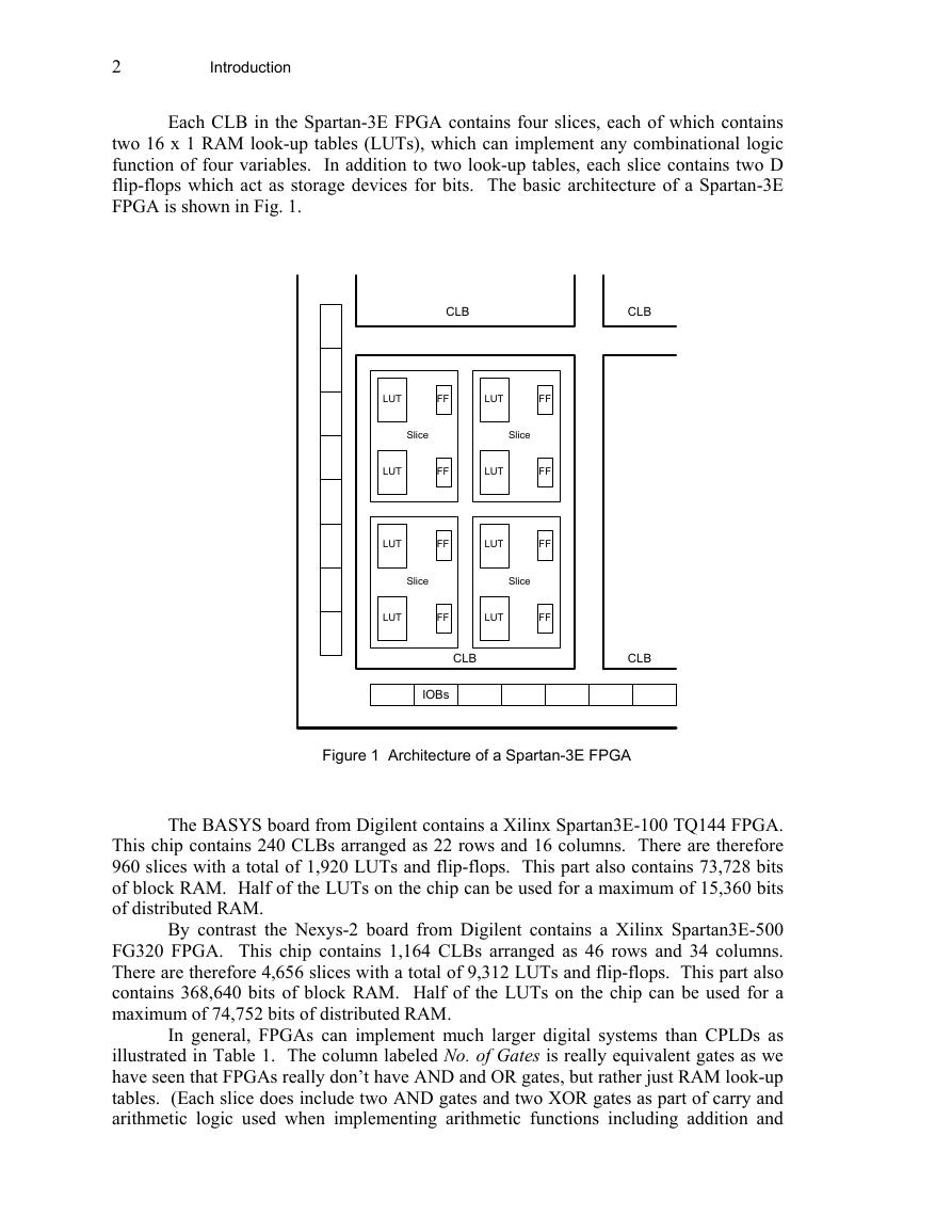
Each CLB in the Spartan-3E FPGA contains four slices, each of which contains
two 16 x 1 RAM look-up tables (LUTs), which can implement any combinational logic
function of four variables. In addition to two look-up tables, each slice contains two D
flip-flops which act as storage devices for bits. The basic architecture of a Spartan-3E
FPGA is shown in Fig. 1.
The BASYS board from Digilent contains a Xilinx Spartan3E-100 TQ144 FPGA.
This chip contains 240 CLBs arranged as 22 rows and 16 columns. There are therefore
960 slices with a total of 1,920 LUTs and flip-flops. This part also contains 73,728 bits
of block RAM. Half of the LUTs on the chip can be used for a maximum of 15,360 bits
of distributed RAM.
Figure 1 Architecture of a Spartan-3E FPGA
By contrast the Nexys-2 board from Digilent contains a Xilinx Spartan3E-500
FG320 FPGA. This chip contains 1,164 CLBs arranged as 46 rows and 34 columns.
There are therefore 4,656 slices with a total of 9,312 LUTs and flip-flops. This part also
contains 368,640 bits of block RAM. Half of the LUTs on the chip can be used for a
maximum of 74,752 bits of distributed RAM.
In general, FPGAs can implement much larger digital systems than CPLDs as
illustrated in Table 1. The column labeled No. of Gates is really equivalent gates as we
have seen that FPGAs really don’t have AND and OR gates, but rather just RAM look-up
tables. (Each slice does include two AND gates and two XOR gates as part of carry and
arithmetic logic used when implementing arithmetic functions including addition and
FF
LUT
IOBs
CLB
Slice
Slice
CLB
�




 2023年江西萍乡中考道德与法治真题及答案.doc
 2012年重庆南川中考生物真题及答案.doc
 2013年江西师范大学地理学综合及文艺理论基础考研真题.doc
 2020年四川甘孜小升初语文真题及答案I卷.doc
 2020年注册岩土工程师专业基础考试真题及答案.doc
 2023-2024学年福建省厦门市九年级上学期数学月考试题及答案.doc
 2021-2022学年辽宁省沈阳市大东区九年级上学期语文期末试题及答案.doc
 2022-2023学年北京东城区初三第一学期物理期末试卷及答案.doc
 2018上半年江西教师资格初中地理学科知识与教学能力真题及答案.doc
 2012年河北国家公务员申论考试真题及答案-省级.doc
 2020-2021学年江苏省扬州市江都区邵樊片九年级上学期数学第一次质量检测试题及答案.doc
 2022下半年黑龙江教师资格证中学综合素质真题及答案.doc