APPLICATION NOTE
Bi-directional level shifter for
I²C-bus and other systems.
AN97055
�
Philips Semiconductors
Bi-directional level shifter for I²C-bus and other
systems.
Application Note
AN97055
Abstract
With a single MOS-FET a bi-directional level shifter circuit can be realised to connect devices with different
supply voltages of e.g. 5 Volt and 3.3 Volt to one I2C-bus system. The level shifter can also isolate a bus
section of powered-down devices from the I2C-bus, allowing the powered part of the I2C-bus to operate in a
normal way.
The level shifter can also be used in other bus systems or point to point connections for level shifting and/or
isolation.
Purchase of Philips I2C components conveys
a license under the I2C patent to use the com-
ponents in the I2C system, provided the system
conforms to the I2C specifications defined by
Philips.
© Philips Electronics N.V. 1997
All rights are reserved. Reproduction in whole or in part is prohibited without the prior written consent of the
copyright owner.
The information presented in this document does not form part of any quotation or contract, is believed to be
accurate and reliable and may be changed without notice. No liability will be accepted by the publisher for any
consequence of its use. Publication thereof does not convey nor imply any license under patent- or other
industrial or intellectual property rights.
2
�
Philips Semiconductors
Bi-directional level shifter for I²C-bus and other
systems.
Application Note
AN97055
APPLICATION NOTE
Bi-directional level shifter for
I²C-bus and other systems.
AN97055
Author:
Philips Semiconductors Systems Laboratory Eindhoven,
Herman Schutte
The Netherlands
Level shifter, bi-directional, I²C-bus, gate way, power-off, protection.
Keywords
Number of pages: 16
Date: 97-08-04
3
�
Philips Semiconductors
Bi-directional level shifter for I²C-bus and other
systems.
Application Note
AN97055
Summary
Present technologies for integrated circuit with clearances of 0.5 m m and less, limit the maximum supply voltage
and consequently the logic levels for the digital I/O signals. To interface these lower voltage circuits with
existing 5 Volt devices a level shifter is needed. For bi-directional bus systems as e.g. the I2C-bus, such a level
shifter must be bi-directional, without the need of a direction control signal. With only one appropriate MOS-FET
for each bus line the desired level shifting with automatic direction control can be done. The levels may have a
vast range, depending on the used MOS-FET, e.g. down to 2 Volt at the “Lower voltage” side and up to 10
Volt or more at the “Higher voltage” side of the level shifter.
An additional function of the level shifter is that it can isolate a powered-down section in a bus system, without
obstructing the powered part. Another feature is the protection of the “Lower voltage” section against high
voltage spikes at the “Higher voltage” section, as long as the MOS-FET can withstand this spikes.
4
�
Philips Semiconductors
Bi-directional level shifter for I²C-bus and other
systems.
Application Note
AN97055
CONTENTS
1. INTRODUCTION .......................................................................................................................................... 7
1.1 References............................................................................................................................................ 7
1.2 World Wide Web. .................................................................................................................................. 7
2. INTERCONNECTION OF DEVICES WITH DIFFERENT LOGIC LEVELS. .................................................. 8
2.1 Logic levels of the I2C-bus. .................................................................................................................... 8
2.2 I2C-bus devices with different supply voltages and 5V tolerant I/O’s. ...................................................... 9
2.3 Devices with different logic levels connected via the bi-directional level shifter. .................................... 10
2.3.1 Description of the level shift operation......................................................................................... 10
2.3.2 Protection of the “Lower voltage” section against high voltage spikes.......................................... 11
2.3.3 The level shifter used in point to point connections...................................................................... 11
2.3.4 Isolation of the powered-down “Lower voltage” section. .............................................................. 11
2.3.5 Extended circuit for isolation of the powered-down “higher voltage” section................................. 12
3. CHARACTERISTICS OF THE MOS-FET’S............................................................................................... 13
4. WAVE FORMS OF THE LOGIC LEVELS................................................................................................... 14
4.1 Shifting from a 3V to a 5V level............................................................................................................ 14
4.2 Shifting from a 5V to a 3V level............................................................................................................ 15
4.3 Wave forms when a bus section is powered-down. .............................................................................. 16
5
�
Philips Semiconductors
Bi-directional level shifter for I²C-bus and other
systems.
Application Note
AN97055
6
�
Philips Semiconductors
Bi-directional level shifter for I²C-bus and other
systems.
Application Note
AN97055
INTRODUCTION
1.
The I2C-bus has been introduced in 1980 by Philips, and has become a de-facto world standard. More than
1000 different IC devices have been provided with an I2C-bus interface, most of them having a 5 Volt supply
voltage and corresponding logic I/O levels. These 5 Volt devices can be interconnected to an I2C-bus system
without any glue logic.
Present technology processes for integrated circuits with clearances of 0.5 m m and less, limit the maximum
supply voltage to 3.3 Volt and in the near future to 2 Volt and less. Also the I/O signals have this limitation, so
there is a problem to interconnect them with existing 5 Volt devices. The same problem will exist in the future to
interconnect e.g. 3.3 Volt devices and 2 Volt devices.
One solution for this problem is the use of 5 Volt tolerant I/O’s. Most present IC technology processes have a
high voltage option to make I/O signals 5V tolerant. This gives the possibility to connect lower voltage devices
to 5 Volt devices or to 5 Volt bus systems. The disadvantage of this 5 Volt option is that it requires more masks
and process steps in the IC manufacturing, which makes the IC devices significantly more expensive.
Another solution is the use of external level shifters. In the different logic families level shifters are available,
most of them for one direction, which cannot be used in a bi-directional bus system. The bi-directional level
shifters in these families require a direction control signal, which is not available in a serial bus system, so these
level shifters are not applicable.
The bi-directional level shifter circuit described in this application note consists of one discrete MOS-FET for
each bus line. In spite of its surprising simplicity, it not only fulfils the requirement of bi-directional level shifting
without a direction control signal, but it also has the next additional features:
- isolating of a powered-down bus section from the rest of the bus system,
- protection of the “Lower voltage” side against high voltage spikes at the ‘Higher voltage” side.
The bi-directional level shifter can be used in standard mode ( 0 to 100 kbit/s) or in fast mode (0 to 400 kbit/s)
I2C-bus systems, without any change. The following description apply for both modes.
References.
1.1
Useful references for I2C-bus related documentation:
•
•
•
The I2C-bus and how to use it. (including specification)
I2C Peripherals, DATA HANDBOOK IC12 (includes I2C-bus spec.)
Application Notes and Development Tools for 80C51 Microcontrollers
(includes I2C-bus application notes, articles and I2C-bus spec.)
ordering inf.
9398 393 40011
9397 750 00306
9397 750 00963
1.2 World Wide Web.
Internet access for Philips Semiconductors:
http://www.semiconductors.philips.com
7
�
Philips Semiconductors
Bi-directional level shifter for I²C-bus and other
systems.
Application Note
AN97055
2.
INTERCONNECTION OF DEVICES WITH DIFFERENT LOGIC LEVELS.
Logic levels of the I2C-bus.
2.1
An overview of the different logic levels, used in I2C-bus systems, is given below.
The I2C-bus specifies two types of logic levels:
a) fixed levels,
b) supply voltage related levels.
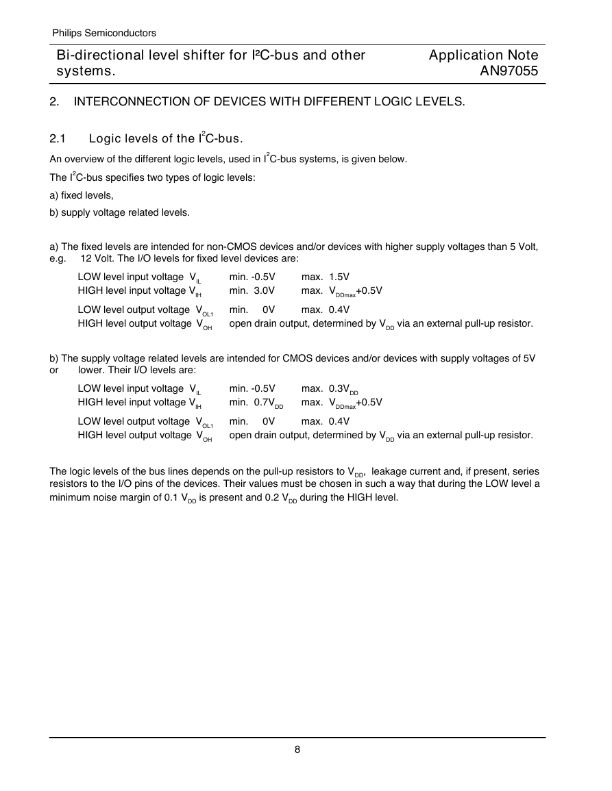
a) The fixed levels are intended for non-CMOS devices and/or devices with higher supply voltages than 5 Volt,
e.g. 12 Volt. The I/O levels for fixed level devices are:
LOW level input voltage VIL
HIGH level input voltage VIH
LOW level output voltage VOL1 min. 0V
HIGH level output voltage VOH
min. -0.5V
min. 3.0V
max. 1.5V
max. VDDmax+0.5V
max. 0.4V
open drain output, determined by VDD via an external pull-up resistor.
b) The supply voltage related levels are intended for CMOS devices and/or devices with supply voltages of 5V
or lower. Their I/O levels are:
LOW level input voltage VIL
HIGH level input voltage VIH
LOW level output voltage VOL1 min. 0V
HIGH level output voltage VOH
min. -0.5V
min. 0.7VDD
max. 0.3VDD
max. VDDmax+0.5V
max. 0.4V
open drain output, determined by VDD via an external pull-up resistor.
The logic levels of the bus lines depends on the pull-up resistors to VDD, leakage current and, if present, series
resistors to the I/O pins of the devices. Their values must be chosen in such a way that during the LOW level a
minimum noise margin of 0.1 VDD is present and 0.2 VDD during the HIGH level.
8
�



 2023年江西萍乡中考道德与法治真题及答案.doc
 2012年重庆南川中考生物真题及答案.doc
 2013年江西师范大学地理学综合及文艺理论基础考研真题.doc
 2020年四川甘孜小升初语文真题及答案I卷.doc
 2020年注册岩土工程师专业基础考试真题及答案.doc
 2023-2024学年福建省厦门市九年级上学期数学月考试题及答案.doc
 2021-2022学年辽宁省沈阳市大东区九年级上学期语文期末试题及答案.doc
 2022-2023学年北京东城区初三第一学期物理期末试卷及答案.doc
 2018上半年江西教师资格初中地理学科知识与教学能力真题及答案.doc
 2012年河北国家公务员申论考试真题及答案-省级.doc
 2020-2021学年江苏省扬州市江都区邵樊片九年级上学期数学第一次质量检测试题及答案.doc
 2022下半年黑龙江教师资格证中学综合素质真题及答案.doc