IEEE TRANSACTIONS ON COMMUNICATIONS, VOL. 41, NO. 3, MARCH 1993
501
Interpolation in Digital
Modems-Part
I: Fundamentals
Floyd M. Gardner, Fellow, IEEE
Abstrucf- Timing adjustment in a digital modem must be
performed by interpolation if sampling is not synchronized to
the data symbols. This paper describes the fundamental equation
for interpolation, proposes a method for control, and outlines the
signal-processing characteristics appropriate to an interpolator.
The material combines a review of previously known topics,
presentation of new results, and a tutorial exposition of the
subject.
A companion paper will treat performance and implementa-
tion.
T the symbols of the incoming data signal. In analog-
IMING in a data receiver must be synchronized to
I. INTRODUCTION
implemented modems, synchronization typically is performed
by a feedback loop that adjusts the phase of a local clock, or
by a feedforward arrangement that regenerates a timing wave
from the incoming signal. The local clock or the timing wave
is used to sample (or strobe) the filtered output of the modem,
once per symbol interval. Message data are recovered from
the strobes. Timing of the strobes is adjusted for optimum
detection of the symbols.
Implementation of the modem by digital techniques (a topic
of intense present activity) introduces sampling of the signal.
In some circumstances, the sampling can be synchronized
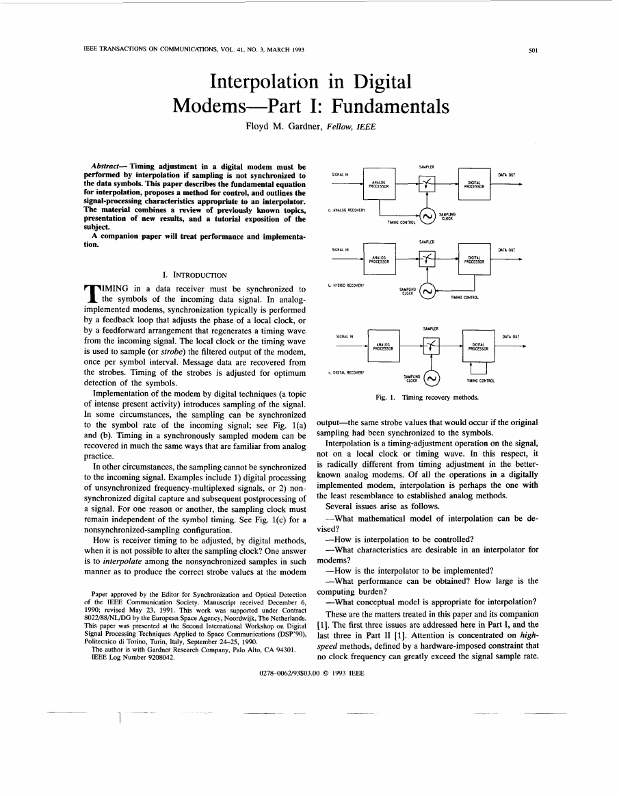
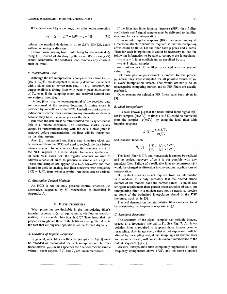
to the symbol rate of the incoming signal; see Fig. l(a)
and (b). Timing in a synchronously sampled modem can be
recovered in much the same ways that are familiar from analog
practice.
In other circumstances, the sampling cannot be synchronized
to the incoming signal. Examples include 1) digital processing
of unsynchronized frequency-multiplexed signals, or 2) non-
synchronized digital capture and subsequent postprocessing of
a signal. For one reason or another, the sampling clock must
remain independent of the symbol timing. See Fig. l(c) for a
nonsynchronized-sampling configuration.
How is receiver timing to be adjusted, by digital methods,
when it is not possible to alter the sampling clock? One answer
is to interpolate among the nonsynchronized samples in such
manner as to produce the correct strobe values at the modem
Paper approved by the Editor for Synchronization and Optical Detection
of the IEEE Communication Society. Manuscript received December 6,
1990; revised May 23, 1991. This work was supported under Contract
8022/88/NL/DG by the European Space Agency, Noordwijk, The Netherlands.
This paper was presented at the Second International Workshop on Digital
Signal Processing Techniques Applied to Space Communications (DSP’90),
Politecnico di Torino, Turin, Italy, September 24-25, 1990.
m e author is with Gardner Research Company, Palo Alto, CA 94301,
IEEE Log Number 9208042.
SIGNAL IN
DATA OUT
PROCESSOR
ANALOG
PROCESSOR
DIGITAL
SAMPLER
0 . ANALOG RECOYCRY
SIGNAL IN
DIGITAL
.
+
ANALOG
DATA OUT
PROCESSOR
-
w
SAMPLING @--I
TIMING CONTROL
PROCESSOR
PROCESSOR
DATA OUT
PROCESSOR
DIGITAL
SIGNAL IN
SAMPLER
ANALOG
b. HYBRID RECOVERY
CLOCK
C. DIGITAL RECOVERY
Fig. 1. Timing
SAMPLING N
CLOCK
recovery methods.
TIMING CONTROL
output-the
sampling had been synchronized to the symbols.
same strobe values that would occur if the original
Interpolation is a timing-adjustment operation on the signal,
not on a local clock or timing wave. In this respect, it
is radically different from timing adjustment in the better-
known analog modems. Of all the operations in a digitally
implemented modem, interpolation is perhaps the one with
the least resemblance to established analog methods.
Several issues arise as follows.
-What mathematical model of interpolation can be de-
vised?
-How
-What
modems?
is interpolation to be controlled?
characteristics are desirable in an interpolator for
-How
-What
is the interpolator to be implemented?
performance can be obtained? How large is the
computing burden?
conceptual model is appropriate for interpolation?
-What
These are the matters treated in this paper and its ‘Ompanion
[l]. The first three issues are addressed here in Part I, and the
last three in Part 11 [I]. Attention is concentrated On high-
‘peed methods, defined by a hardware-imposed constraint that
no clock frequency can greatly exceed the signal sample rate.
027&0062/93$03.00 0 1993 IEEE
�
502
IEEE TRANSACTIONS ON COMMUNICATIONS, VOL. 41, NO. 3, MARCH 1993
11. BACKGROUND
Interpolation as a Digital Signal Processing (DSP) opera-
tion has been covered extensively in the literature; excellent
examples and further references may be found in [2] and [3].
By contrast, the role of interpolation in timing adjustment has
had comparatively meager attention [2, ch. 61, [4], [5]. In fact,
these latter references do not speak of “interpolation”, but of
“digital phase shifting” [2, ch. 61 and [4], or of “sampling-rate
conversion” [2, ch. 21 and [5].
It will be seen presently that the process of timing adjust-
ment includes substantially more than interpolation alone and
that “rate conversion” is a more accurate label. Nonetheless,
we will apply the term “interpolation” to denote all of the
processes that are involved in adjustment of timing.
The term “interpolation” to describe the entire timing-
adjustment process appears to have been published first by
a group at the Technical University of Aachen [6], [7]. The
term is also used by Bingham [8, p. 1671.
In light of the extensive DSP literature on interpolation,
and of the large number of digitally implemented modems
that have been built for voice-frequency telephone-line service,
how is it that the literature on digital timing adjustment is so
sparse?
Authors in the established DSP literature almost invariably
restrict themselves to sampling-rate conversion by a rational
factor, which can be modeled as a cascade of interpolation
and decimation, each by integer ratios. Thus, the output is
synchronized to the input.
But the inherent problem of fully digital timing adjustment
is that the signal sampling is not synchronized to the symbol
timing; the two rates are incommensurate and the sample times
never coincide exactly with desired strobe times. Recognition
of incommensurability is vital to understanding the timing-
adjustment problem.
Limitations of the DSP literature aside, why didn’t the
timing adjustment problem arise more clearly in the design
of digitally implemented telephone-line modems? The answer
is that it indeed did arise, and was solved by the adaptive
equalizers that play so large a role in those modems. Besides
correcting for transmission dispersion, an equalizer almost
incidentally also corrects the timing. For that reason, timing
adjustment itself does not appear as a widely recognized,
distinct problem in the context of telephone-line modems.
Digital implementation is now coming to higher speed com-
munications links which do not require adaptive equalization.
The need for digital timing adjustment must be faced by itself,
without embedding it inside an equalizer.
111. MODEL
A. Timing Loop
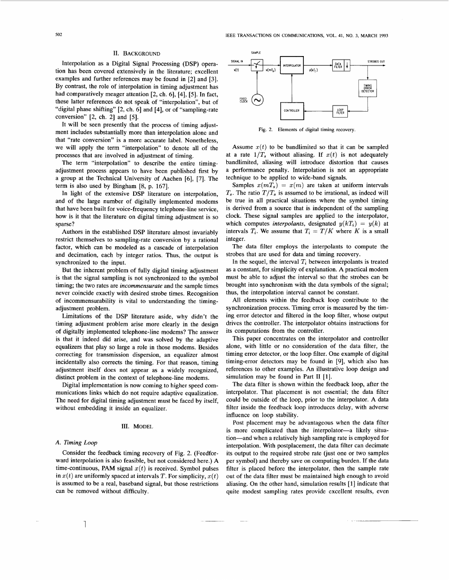
Consider the feedback timing recovery of Fig. 2. (Feedfor-
ward interpolation is also feasible, but not considered here.) A
time-continuous, PAM signal z(t) is received. Symbol pulses
in z ( t ) are uniformly spaced at intervals T . For simplicity, z ( t )
is assumed to be a real, baseband signal, but those restrictions
can be removed without difficulty.
1
SAMPLE
&
I
CLOCK
FIXED
I
TIMING
ERROR
DETECTOR
Fig. 2. Elements of digital timing recovery.
Assume ~ ( t )
to be bandlimited so that it can be sampled
at a rate l/Ts without aliasing. If z(t) is not adequately
bandlimited, aliasing will introduce distortion that causes
a performance penalty. Interpolation is not an appropriate
technique to be applied to wide-band signals.
Samples z(mT,) = z(m) are taken at uniform intervals
T,. The ratio T/Ts is assumed to be irrational, as indeed will
be true in all practical situations where the symbol timing
is derived from a source that is independent of the sampling
clock. These signal samples are applied to the interpolator,
which computes interpolants, designated y(lcTi) = y(k) at
intervals Ti. We assume that Ti = T / K where K is a small
integer.
The data filter employs the interpolants to compute the
strobes that are used for data and timing recovery.
In the sequel, the interval Ti between interpolants is treated
as a constant, for simplicity of explanation. A practical modem
must be able to adjust the interval so that the strobes can be
brought into synchronism with the data symbols of the signal;
thus, the interpolation interval cannot be constant.
All elements within the feedback loop contribute to the
synchronization process. Timing error is measured by the tim-
ing error detector and filtered in the loop filter, whose output
drives the controller. The interpolator obtains instructions for
its computations from the controller.
This paper concentrates on the interpolator and controller
alone, with little or no consideration of the data filter, the
timing error detector, or the loop filter. One example of digital
timing-error detectors may be found in [9], which also has
references to other examples. An illustrative loop design and
simulation may be found in Part I1 [l].
The data filter is shown within the feedback loop, after the
interpolator. That placement is not essential; the data filter
could be outside of the loop, prior to the interpolator. A data
filter inside the feedback loop introduces delay, with adverse
influence on loop stability.
Post placement may be advantageous when the data filter
is more complicated than the interpolator-a
likely situa-
tion-and when a relatively high sampling rate is employed for
interpolation. With postplacement, the data filter can decimate
its output to the required strobe rate (just one or two samples
per symbol) and thereby save on computing burden. If the data
filter is placed before the interpolator, then the sample rate
out of the data filter must be maintained high enough to avoid
aliasing. On the other hand, simulation results [ l ] indicate that
quite modest sampling rates provide excellent results, even
�
GARDNER: INTERPOLATION IN DIGITAL MODEMS-PART
I
503
Analog
Impulses
Analog
Interpolated
Signal
Samples
x h T s )
c DAC
Interpolants
c
Y(kTi )
Froctionol
INPUT SAMPLE TIMES
Rerample
at t = kTi
(k-l)T;
/ '"
brepoint
Index
OUTPUT SAMPLE IlYES
(k+l)T;
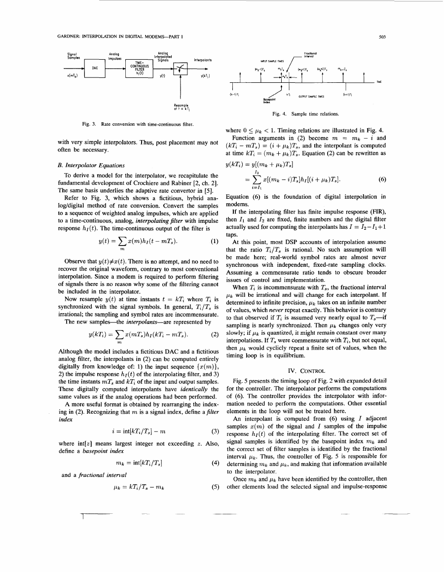
Fig. 4. Sample time relations.
Fig. 3. Rate conversion with time-continuous filter.
with very simple interpolators. Thus, post placement may not
often be necessary.
B. Interpolator Equations
To derive a model for the interpolator, we recapitulate the
fundamental development of Crochiere and Rabiner [2, ch. 21.
The same basis underlies the adaptive rate convertor in [5].
Refer to Fig. 3, which shows a fictitious, hybrid ana-
loddigital method of rate conversion. Convert the samples
to a sequence of weighted analog impulses, which are applied
to a time-continuous, analog, interpolating filter with impulse
response hI(t). The time-continuous output of the filter is
Observe that y(t)#z(t). There is no attempt, and no need to
recover the original waveform, contrary to most conventional
interpolation. Since a modem is required to perform filtering
of signals there is no reason why some of the filtering cannot
be included in the interpolator.
Now resample y(t) at time instants t = kTi where Ti is
synchronized with the signal symbols. In general, T;/T, is
irrational; the sampling and symbol rates are incommensurate.
represented by
The new samples-the
interpolants-are
y(kT;) = E z ( m T , ) h I ( k T i - mT,).
(2)
m
Although the model includes a fictitious DAC and a fictitious
analog filter, the interpolants in (2) can be computed entirely
digitally from knowledge of 1) the input sequence {z(m)},
2) the impulse response hl(t) of the interpolating filter, and 3 )
the time instants mT, and kTi of the input and output samples.
These digitally computed interpolants have identically the
same values as if the analog operations had been performed.
A more useful format is obtained by rearranging the index-
ing in (2). Recognizing that m is a signal index, define a filter
index
z = int[kTi/T,] - m
(3)
where int[z] means largest integer not exceeding z. Also,
define a basepoint index
and a fractional interval
where 0 5 ,c& < 1. Timing relations are illustrated in Fig. 4.
Function arguments in (2) become m = m k - i and
(kT; - mT,) = (z + pk)T,, and the interpolant is computed
at time kT; = (mk + pk)Ts. Equation (2) can be rewritten as
Equation (6) is the foundation of digital interpolation in
modems.
If the interpolating filter has finite impulse response (FIR),
then I1 and 12 are fixed, finite numbers and the digital filter
actually used for computing the interpolants has I = 12 -11 + 1
taps.
At this point, most DSP accounts of interpolation assume
that the ratio Ti/T, is rational. No such assumption will
be made here; real-world symbol rates are almost never
synchronous with independent, fixed-rate sampling clocks.
Assuming a commensurate ratio tends to obscure broader
issues of control and implementation.
When Ti is incommensurate with T,, the fractional interval
p k will be irrational and will change for each interpolant. If
determined to infinite precision, PI, takes on an infinite number
of values, which never repeat exactly. This behavior is contrary
to that observed if Ti is assumed very nearly equal to T,-if
sampling is nearly synchronized. Then fik changes only very
slowly; if p k is quantized, it might remain constant over many
interpolations. If T, were commensurate with Ti, but not equal,
then jLk would cyclicly repeat a finite set of values, when the
timing loop is in equilibrium.
IV. CONTROL
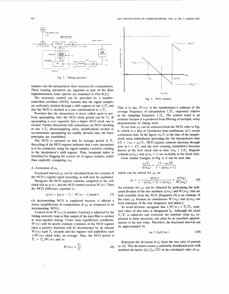
Fig. 5 presents the timing loop of Fig. 2 with expanded detail
for the controller. The interpolator performs the computations
of (6). The controller provides the interpolator with infor-
mation needed to perform the computations. Other essential
elements in the loop will not be treated here.
An interpolant is computed from (6) using I adjacent
samples z(m) of the signal and I samples of the impulse
response hI(t) of the interpolating filter. The correct set of
signal samples is identified by the basepoint index mk and
the correct set of filter samples is identified by the fractional
interval p k . Thus, the controller of Fig. 5 is responsible for
determining mk and pk, and making that information available
to the interpolator.
Once mk and p k have been identified by the controller, then
other elements load the selected signal and impulse-response
�
504
IEEE TRANSACTIONS ON COMMUNICATIONS, VOL. 41, NO. 3, MARCH 1993
I
-
, .................
...................................................
C O N R O U t R
Fig. 5. Timing processor.
I
1-
0
samples into the interpolation filter structure for computations.
These loading operations are regarded as part of the filter
implementation; some options are examined in Part I1 [ 13.
The necessary control can be provided by a number-
controlled oscillator (NCO). Assume that the signal samples
are uniformly clocked through a shift register at rate l/Ts -and
that the NCO is clocked at a rate synchronized to l / T s .
Provided that the interpolator is never called upon to per-
form upsampling’ then the NCo ‘lock period can be Ts‘ If
upsampling is ever required, then a higher NCO clock rate is
needed. Further discussion will concentrate on NCO clocking
at rate l/Ts (downsampling only); modifications needed to
accommodate upsampling are readily devised once the basic
principles are established.
The NCO is operated so that its average period is T,.
Recycling of the NCO register indicates that a new interpolant
is to be computed, using the signal samples currently residing
in the interpolator’s shift register. Thus, basepoint index is
identified by flagging the correct set of signal samples, rather
than explicitly computing mk.
A. Extraction of / l k
Fractional interval lLk can be calculated from the contents of
the NCO’s register upon recycling, as will now be explained.
Designate the NCO register contents computed at the mth
clock tick as q(m), and the NCO control word as W ( m ) . Then
the NCO difference equation is
(
1
[a positive
~
control word ~
~ ( m ) = [q(m - 1) - W ( m - l)]mod-1.
(7)
(A decrementing NCO is employed because
it affords a
minor simplification in computation of /Lk as compared to an
incrementing NCO.)
(
~
is adjusted by the
timing-recovery loop so that output of the data filter is strobed
at near-optimal timing. Under loop equilibrium conditions,
~
will be nearly constant. Contents of the NCO register
(also a positive fraction) will be decremented by an amount
W ( m ) each Ts seconds and the register will underflow each
l / W ( m ) clock ticks, on average. Thus, the NCO period is
T, = T s / W ( m ) and so
1
TS
W(m,) E -.
T,
(8)
I
....................
r l ( m k i l ) - r
(m kt
I
Fig. 6. NCO relations.
That is to say, W ( m ) is the synchronizer’s estimate of the
average frequency of interpolation l/T,, expressed relative
to the sampling frequency l / T s . The control word is an
estimate because it is produced from filtering of multiple, noisy
measurements of timing error.
To see how / L k can be extracted from the NCO, refer to Fig.
6, which is a plot of (fictitious) time-continuous q(t) versus
continuous time. In the figure, mkTs is the time of the sample-
clock pulse immediately preceding the kth interpolation time
ICT, = ( m k + pk)TS. NCO register contents decrease through
zero at t = ICT,, and the zero crossing (underflow) becomes
known at the next clock tick at time ( m k + l)Ts. Register
contents q ( m k ) and q ( m k + 1) are available at the clock ticks.
From similar triangles in Fig. 6, it can be seen that
/IkTs - (1 -Pk)Ts
- -
‘V(mk) 1 - V(m,k f 1 )
which can be solved for pk as
/Lk =
1 - q(mk + 1 ) + q(mk) - w ( m k )
V ( m k )
-
An estimate for P k can be obtained by performing the indi-
cated division of the two numbers q ( m k ) and W(mk) that are
both available from the NCO. [Equation (9) is an estimate of
the exact /Lk because its constituents W(mk) and q ( m k ) are
’0th estimates of the true frequency and phase.]
To avoid division, recognize that l / W ( m ) 2~ T,/Ts; nom-
inal value of this ratio is designated to. Although the exact
/ T ~ is unknown and
(09 ex-
pressed to finite precision, can often be an excellent approxi-
mation to the true value. Therefore, the fractional interval can
be approximated by
the
P k E EOQ(mk).
(10)
Represent the deviation in Eo from the true ratio of periods
as A[. This deviation causes a uniformly distributed error with
standard deviation A [ / ( [ o O )
in the calculated value of p k .
�
GARDNER: INTERPOLATION IN DIGITAL MODEMCPART
I
If the deviation of [ O is too large, then a first order correction
reduces the standard deviation in pk to at2/([;fi), again
without requiring a division.
Timing errors arising from multiplying by the nominal
506
IEEE TRANSACTIONS ON COMMUNICATIONS, VOL. 41, NO. 3, MARCH 1993
0 ) Spectrum of x(t)
b) Spectrum of x(mT,)
c) Spectrum of y(t)
d) Folded Spectrum of y(kTi)
Fig. 7. Signal spectra.
behavior is desirable in a practical interpolation filter. Of
course, no realizable filter can provide infinite attenuation over
an entire stopband. Therefore, any practical filter will introduce
some penalty because of incomplete suppression of images.
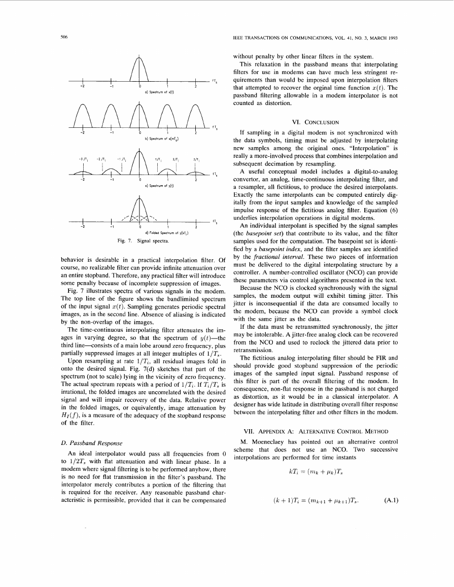
Fig. 7 illustrates spectra of various signals in the modem.
The top line of the figure shows the bandlimited spectrum
of the input signal ~ ( t ) . Sampling generates periodic spectral
images, as in the second line. Absence of aliasing is indicated
by the non-overlap of the images.
The time-continuous interpolating filter attenuates the im-
ages in varying degree, so that the spectrum of y(t)-the
third line-consists of a main lobe around zero frequency, plus
partially suppressed images at all integer multiples of l/Ts.
Upon resampling at rate l/Ti, all residual images fold in
onto the desired signal. Fig. 7(d) sketches that part of the
spectrum (not to scale) lying in the vicinity of zero frequency.
The actual spectrum repeats with a period of l/Ti. If T,/T, is
irrational, the folded images are uncorrelated with the desired
signal and will impair recovery of the data. Relative power
in the folded images, or equivalently, image attenuation by
H r ( f ) , is a measure of the adequacy of the stopband response
of the filter.
without penalty by other linear filters in the system.
This relaxation in the passband means that interpolating
filters for use in modems can have much less stringent re-
quirements than would be imposed upon interpolation filters
that attempted to recover the orginal time function ~ ( t ) . The
passband filtering allowable in a modem interpolator is not
counted as distortion.
VI. CONCLUSION
If sampling in a digital modem is not synchronized with
the data symbols, timing must be adjusted by interpolating
new samples among the original ones. “Interpolation” is
really a more-involved process that combines interpolation and
subsequent decimation by resampling.
A useful conceptual model includes a digital-to-analog
convertor, an analog, time-continuous interpolating filter, and
a resampler, all fictitious, to produce the desired interpolants.
Exactly the same interpolants can be computed entirely dig-
itally from the input samples and knowledge of the sampled
impulse response of the fictitious analog filter. Equation (6)
underlies interpolation operations in digital modems.
An individual interpolant is specified by the signal samples
(the basepoint set) that contribute to its value, and the filter
samples used for the computation. The basepoint set is identi-
fied by a basepoint index, and the filter samples are identified
by the fractional interval. These two pieces of information
must be delivered to the digital interpolating structure by a
controller. A number-controlled oscillator (NCO) can provide
these parameters via control algorithms presented in the text.
Because the NCO is clocked synchronously with the signal
samples, the modem output will exhibit timing jitter. This
jitter is inconsequential if the data are consumed locally to
the modem, because the NCO can provide a symbol clock
with the same jitter as the data.
If the data must be retransmitted synchronously, the jitter
may be intolerable. A jitter-free analog clock can be recovered
from the NCO and used to reclock the jittered data prior to
retransmission.
The fictitious analog interpolating filter should be FIR and
should provide good stopband suppression of the periodic
images of the sampled input signal. Passband response of
this filter is part of the overall filtering of the modem. In
consequence, non-flat response in the passband is not charged
as distortion, as it would be in a classical interpolator. A
designer has wide latitude in distributing overall filter response
between the interpolating filter and other filters in the modem.
D. Passband Resvonse
An ideal interpolator would pass all frequencies from 0
to 1/2T, with flat attenuation and with linear phase. In a
modem where signal filtering is to be performed anihow, there
is no need for flat transmission in the filter’s passband. The
interpolator merely contributes a portion of the filtering that
is required for the receiver. Any reasonable passband char-
acteristic is permissible, provided that it can be compensated
VII. APPENDIX A: ALTERNATIVE CONTROL METHOD
M. Moeneclaey has pointed out an alternative control
that does not use an NCO. Two successive
scheme
interpolations are performed for time instants
kT, = VI,^: + pk)T,
( k + l)Tz = ( ~ + + i + pk+i)Ts.
�
GARDNER: INTERPOLATION IN DIGITAL MODEMS-PART
I
507
Subtracting these two expressions and rearranging slightly
gives the recursion
pk - / L k + l .
mk+l = mk Ti/Ts
(-4.2)
By definition, mk+l is an integer. Then, since 0 5 p k + l < 1,
(-4.3)
whence the increment in sample count from one interpolation
to the next is
mk+l + pk+l = mk 4- Ti/Ts + pk < m k + 2
Notice that a practical scheme must work with the increment
rather than the sample count mk. Any finite-length counter of
mk would overflow eventually.
To compute the fractional interval PIE, recognize that the
fractional part fp[ ] of the increment is zero
from which one may conclude
The true Ti/T, is not available. Instead, the synchronizer
produces a control word V(mk) N TiIT, to be used in
the recursions (A.4) and (AS). This control word is the
synchronizer’s estimate of the true interpolation period Ti
relative to the sampling period T,.
The alternative control method may be most useful in
systems where the data are consumed at the same location
as the data receiver, without reclocking. It is not immediately
apparent how a jitter-free, time-continuous clock for retrans-
mission could be synthesized easily without the phase v(m)
that accumulates in an NCO.
ACKNOWLEDGMENT
I wish to thank Dr. R. Harris and L. Erup of the European
Space Agency for their helpful critiques of the work as it
progressed.
REFERENCES
L. Erup, F. M. Gardner, and R. A. Harris, “Interpolation in digital
11: implementation and performance,” to be published.
modems-Part
R. E. Crochiere and L. R. Rabiner, Multirate Digital Signal Processing.
Englewood Cliffs, NJ: Prentice-Hall, 1983.
R. W. Schafer and L. R. Rabiner, “A digital signal processing approach
to interpolation,” Proc. IEEE, vol. 61, pp. 692-702, June 1973.
R. E. Crochiere, L. R. Rabiner, and R. R. Shively, “A novel imple-
mentation of digital phase shifters,” Bell Syst. Tech. J., vol. 54, pp.
1497-1502, Oct. 1975.
F. Takahata et al., “A PSK group modem for satellite communication,”
IEEE J. Select. Areas Commun., vol. SAC-5, pp. 648-661, May 1987.
M. Oerder, G. Ascheid, R. Haeb, and H. Meyr, “An all digital implemen-
tation of a receiver for bandwidth efficient communication,” in Signal
Processing III (Eusipco 1986), I. T. Young et al. Ed., pp. 1091-1094,
Elsevier, 1986.
G. Ascheid, M. Oerder, J. Stahl, and H. Meyr, “An all digital receiver
architecture for bandwidth efficient transmission at high data rates,”
IEEE Trans. Commun., vol. 37, pp. 804-813, Aug. 1989.
J. A. C. Bingham, The Theory and Practice of Modem Design. New
York: Wiley, 1988.
F. M. Gardner, “A BPSWQPSK timing-error detector for sampled
receivers,” IEEE Trans. Commun., vol. COM-34, pp. 423-429, May
1986.
E. Auer, “An advanced, variable data rate modem for Intelsat IDR/IBS
services,” Paper 1-3, Proc. 2nd In?. Workshop Digital Signal Processing
Techniques Appl. Space Commun., Turin, Italy, 24-25 Sept. 1990.
Floyd M. Gardner (S’49-A’54-SM’58-F’80)
re-
ceived the B.S.E.E. degree from the Illinois Institute
of Technology, Chicago, IL, in 1950, the M.S.E.E.
from Stanford University, Stanford, CA, in 1951,
and the Ph.D. degree from the University of Illinois,
Urbana, IL, 1953.
He has been a independent consulting engineer
since 1960, active in the fields of communications
and electronics. He is a specialist in synchronization
and in phase-lock loops, and is the author of the
book Phaselock Techniques (New York: Wiley, 2nd
edition, 1979). In recent years he has been investigating algorithms for
digitally implemented modems.
Dr. Gardner is a Registered Professional Engineer in the State of California.
�


 2023年江西萍乡中考道德与法治真题及答案.doc
 2012年重庆南川中考生物真题及答案.doc
 2013年江西师范大学地理学综合及文艺理论基础考研真题.doc
 2020年四川甘孜小升初语文真题及答案I卷.doc
 2020年注册岩土工程师专业基础考试真题及答案.doc
 2023-2024学年福建省厦门市九年级上学期数学月考试题及答案.doc
 2021-2022学年辽宁省沈阳市大东区九年级上学期语文期末试题及答案.doc
 2022-2023学年北京东城区初三第一学期物理期末试卷及答案.doc
 2018上半年江西教师资格初中地理学科知识与教学能力真题及答案.doc
 2012年河北国家公务员申论考试真题及答案-省级.doc
 2020-2021学年江苏省扬州市江都区邵樊片九年级上学期数学第一次质量检测试题及答案.doc
 2022下半年黑龙江教师资格证中学综合素质真题及答案.doc