Application Report
SLAA486A–March 2011
EKG-Based Heart-Rate Monitor Implementation on the
LaunchPad Value Line Development Kit Using the
MSP430G2452 MCU
Abhishek Joshi, Sourabh Ravindran and Austin Miller .......................................... MSP430 System Solutions
ABSTRACT
This application report describes a low-cost heart-rate monitor solution based on the MSP430™
LaunchPad Value Line Development Kit (MSP-EXP430G2), which uses the MSP430G2xx microcontroller
(MCU). A daughterboard amplifies and filters the electrocardiogram (EKG) signal before it is sent to the
MCU for sampling and processing. The heartbeat-per-minute data is sent to the PC by means of the
back-channel UART-over-USB available on the LaunchPad. Additionally, an eZ430 radio frequency (RF)
target can be connected to the six-pin header on the daughterboard to transmit data wirelessly via the
SimpliciTI™ network protocol. The system can be powered by either universal serial bus (USB) power, a
CR2032 3-V coin cell, or two AA or AAA batteries.
WARNING
The application presented here is for reference design purposes
only and is not intended for any life-saving or medical-monitoring
use.
Project collateral and source code discussed in this application report can be downloaded from the
following URL:
http://software-dl.ti.com/msp430/msp430_public_sw/mcu/msp430/EKG-Based-Heart-Rate-
Monitor/1_00_00_00/index_FDS.html.
Contents
Introduction .................................................................................................................. 2
1
Hardware Description ...................................................................................................... 3
2
Software ...................................................................................................................... 6
3
References ................................................................................................................... 7
4
Amplifier Options ................................................................................................... 8
Appendix A
Appendix B Wired USB Demo With Back-Channel UART ................................................................ 10
Appendix C Wireless UART Demo With the eZ430 RF Target Board ................................................... 11
Hardware Schematic Diagrams ................................................................................. 12
Appendix D
List of Figures
1
2
3
4
5
6
Human Heart Anatomy (left) and EKG Waveform (right) .............................................................. 2
Hand Detection Circuit Diagram .......................................................................................... 3
Software Flowchart ........................................................................................................ 6
Heart-Rate Monitor Setup (left) and UART Output on PC (right)..................................................... 7
Hardware Schematic Diagram (Page 1/2) ............................................................................. 12
Hardware Schematic Diagram (Page 2/2) ............................................................................. 13
List of Tables
SLAA486A–March 2011
Submit Documentation Feedback
EKG-Based Heart-Rate Monitor Implementation on the LaunchPad Value Line
Development Kit Using the MSP430G2452 MCU
1
© 2011, Texas Instruments Incorporated
�
Introduction
1
2
3
4
5
6
www.ti.com
LaunchPad Port/Pin Functionality Mapping – Left Header ............................................................ 4
LaunchPad Port/Pin Functionality Mapping – Right Header .......................................................... 4
Supply Current Consumption.............................................................................................. 5
Instrumentation Amplifier Comparison ................................................................................... 8
Operational Amplifier Comparison........................................................................................ 9
eZ430 RF Target Boards ................................................................................................. 11
1
Introduction
The source of the human heart beat is an electrical pulse generated by a cluster of cells within the heart
called the sinoatrial (SA) node [1]. This pulse travels from the SA node through the surrounding cells of
the heart and then to the atrioventricular (AV) node. The AV node acts as a gate that allows the atria to
finish contraction before allowing the pulse to move on to the ventricles. Each atrium pumps blood to a
corresponding ventricle. The right atrium pumps blood to the right ventricle to provide blood to the lungs.
The left ventricle, sourced by the left atrium, is the chamber that pumps blood throughout the body.
Figure 1. Human Heart Anatomy (left) and EKG Waveform (right)
The electrocardiogram (ECG) or elektrokardiogramm (EKG) is a medical standard for testing the human
heart for defects and diseases [2]. Figure 1 shows the anatomy of the human heart and the waveform of
the EKG signal. The EKG waveform can be used for extrapolation of data such as the number of
heartbeats per minute (BPM) and the values can range from 30 to 200 BPM or 0.5 to 4 Hz.
The typical amplitude of the R wave component of the EKG signal is approximately 1 mV [3]. This peak is
located within a group of peaks known as the QRS complex and represents the electrical pulse flowing
through the ventricles. As this pulse travels via the blood stream, it can be detected at various points on
the body. The extremities and the chest have become the standard locations for placing electrodes for
acquiring the EKG signal. In this application, the subject’s finger tips act as the differential point of contact
with conductive pads to detect the EKG signal.
MSP430, SimpliciTI, Code Composer Studio are trademarks of Texas Instruments.
IAR Embedded Workbench is a trademark of IAR Systems AB.
All other trademarks are the property of their respective owners.
2
EKG-Based Heart-Rate Monitor Implementation on the LaunchPad Value Line
Development Kit Using the MSP430G2452 MCU
SLAA486A–March 2011
Submit Documentation Feedback
© 2011, Texas Instruments Incorporated
PQRSTTIMEDifferential VoltageBetween Two ElectrodesAtriaDepolarizeVentriclesRepolarizeVentriclesDepolarize1 mVAortaLeftAtriumAtrioventricularNodeLeftVentricleHeartMuscleSinoatrialNodeRightAtriumRightVentricle�
www.ti.com
Hardware Description
2
Hardware Description
The hardware is a daughterboard design attachable to the 10-pin headers on the LaunchPad development
kit. The daughterboard contains the analog front-end components, battery connectors, headers, etc.,
whereas, the MSP430 MCU, the back-channel UART, and the eZ430 emulator circuit with the USB
connector reside on the LaunchPad itself [4]. The schematic diagram of the hardware is shown in
Appendix D.
2.1 Hand Detection Circuit
A resistor divider scheme is implemented to detect contact of the subject’s finger tips with the conductive
pads. The premise of this scheme is that the resistance of the human body between the finger tips is in
the 100 kΩ to 300 kΩ range, and the resistance placed between the conductive pads is significantly
greater than this range, as shown in Figure 2.
Figure 2. Hand Detection Circuit Diagram
When contact is made, the current flows through the path of least resistance (the human body) causing
the voltage at the left conductive pad to change. This voltage is sampled by an analog-to-digital converter
(ADC) channel and the digital conversion result is compared against a set of thresholds to determine
good, bad, or no contact. Power and ground are supplied from the microcontroller pins and can be
disconnected to minimize supply current consumption in sleep mode.
2.2 Analog Front End (AFE)
As mentioned previously, the amplitude of the EKG signal is approximately 1 mV peak-to-peak. The noise
signals picked up by the human body (such as the 50 to 60-Hz line frequency) pose a serious problem to
detecting the low-frequency low-magnitude EKG signal. An analog front end with a high gain with low
cutoff filter frequency is necessary to condition this signal for digital conversion and processing. Because
the common-mode signals from the conductive pads are the same, a differential amplifier simply cancels
out the common-mode and amplifies the input differential EKG signal. The INA332 instrumentation
amplifier is a low-cost differential amplifier used in this application and has a common mode rejection ratio
(CMRR) specification of 73 dB up to 10 kHz, quiescent current of 490 μA, and shutdown current levels
less than 1 μA. It can operate to a minimum supply voltage of 2.7 V with a dedicated shutdown pin.
Additional instrumentation amplifier options relevant to this application are summarized in [3].
The INA332 is configured to a gain of 10 V/V with external 0.1% 10-kΩ resistors. The conductive pads are
connected to the inputs with 51-kΩ resistors in series to limit the current from the human body and also
act as a RC low-pass filter. The 5-MΩ pulldown resistors from the pads to common mode voltage (VCM)
help keep the voltage identical on both inputs and also provide a dc bias point for circuit operation. The
VCM voltage is generated by a general-purpose op-amp in the voltage-follower (low-output impedance)
configuration to 750 mV.
The TLV274 is a quad operational amplifier (op-amp) used in this application with supply currents of 550
μA/channel and minimum supply voltage of 2.7 V. With a CMRR of 58 dB, the op-amps are used to
implement a second-order Sallen-Key low pass filter (LPF) with gain of each stage at 8.5 V/V. The overall
gain of the AFE is 10 X 8.5 X 8.5 = 722.5 V/V, and the cutoff frequency is 16 Hz. Additional
general-purpose op-amp options relevant to this application are also summarized in Heart-Rate and EKG
Monitor Using the MSP430FG439 (SLAA280) [3].
The resulting amplified and conditioned EKG signal output from the LPF is fed to the ADC channel of the
MSP430 microcontroller for conversion and processing. The shutdown pin of the INA332 and the VCC pin
of the TLV274 are connected to one general-purpose input/output (GPIO) pin of the MSP430 to enable or
disable the AFE. The GPIO pin is set to a low state to minimize supply current consumption in sleep
mode. As a precautionary measure, the AFE has protection diodes (TPD2E001) on the conductive pads to
prevent human electrostatic discharge (ESD) from causing component failure.
SLAA486A–March 2011
Submit Documentation Feedback
EKG-Based Heart-Rate Monitor Implementation on the LaunchPad Value Line
Development Kit Using the MSP430G2452 MCU
3
© 2011, Texas Instruments Incorporated
R2MΩRRLeftPadRightPad5MΩ1MΩVDD�
Hardware Description
www.ti.com
2.3
LaunchPad Port/Pin to Functionality Mapping
The LaunchPad Development Kit has a 20-pin PDIP socket that a 14-pin or a 20-pin MCU can be plugged
into. The MSP430G2452 was used for this application and has 8 KB of Flash, 256 B of RAM, 1 Timer_A3
and 8-channel ADC10 [11]. The LaunchPad port/pin mapping is designed to match the pinout of the
MSP430G2xx family of devices.
The port/pin functionality mapping for the left and right header pins on the LanchPad are shown in Table 1
and Table 2, respectively.
Table 1. LaunchPad Port/Pin Functionality Mapping – Left Header
Port/Pin Name
VCC
P1.0 (LED1)
P1.1 (TXD)
P1.2 (RXD)
P1.3 (S2)
P1.4
P1.5
P2.0
P2.1
P2.2
(1) Not used in this application.
Signal Name
VDD
LED_RED
UART_TXD
UART_RXD
P1_3 (SW2)
EKG
HAND_LEFT
N/A (1)
N/A (1)
N/A (1)
Description
Power (VDD) for the MSP430
Indicates bad contact
UART transmit (TX) line
UART receive (RX) line
Push button switch
Input to the ADC to sample filtered and amplified EKG signal
Input to the ADC to sample hand-detection circuit signal
N/A (1)
N/A (1)
N/A (1)
Table 2. LaunchPad Port/Pin Functionality Mapping – Right Header
Port/Pin Name
GND
XIN
XOUT
TEST
(S1) RST
P1.7
(LED2) P1.6
P2.5
P2.4
P2.3
(1) Not used in this application.
Signal Name
GND
P2_6
SHUTDOWN
TEST
RESET (SW1)
P1_7
LED_GREEN
N/A (1)
N/A (1)
N/A (1)
Description
Ground (GND) for the MSP430
VDD for hand detection circuit
Enable/disable the AFE
Spy-Bi-Wire programming pin for the MSP430
Reset switch for the MSP430 (Spy-Bi-Wire programming pin)
GND for hand detection circuit
Indicates good contact
N/A (1)
N/A (1)
N/A (1)
2.4
eZ430 RF Target Header
The hardware has a six-pin header that has power/ground connections and UART lines coming from the
LaunchPad. This header allows for an eZ430 RF target such as the eZ430-RF2500 to be connected for
wireless data transmission [5]. Appendix C has details on target boards with different frequencies and the
SimpliciTI wireless UART demo software for programming them that are provided with this application
report.
2.5 Power Supply Setup
With the daughterboard attached to the LaunchPad, there are multiple ways of powering up the system.
NOTE: The system is designed to be powered from only one power source at a time. The system
should be powered from either USB or coin-cell or 2x AA or 2x AAA batteries.
4
EKG-Based Heart-Rate Monitor Implementation on the LaunchPad Value Line
Development Kit Using the MSP430G2452 MCU
SLAA486A–March 2011
Submit Documentation Feedback
© 2011, Texas Instruments Incorporated
�
www.ti.com
Hardware Description
USB Power:
1. Populate all of the jumpers on the LaunchPad (VCC, RXD, TXD, TEST, RST).
2. Remove the jumper JP1 on the daughterboard.
3. Connect the micro-USB cable from the LaunchPad to the PC. The 5 V from USB supply goes through
a 3.3 V LDO and powers the whole system. The USB cable also serves as a MSP430 application
UART connection to the PC [4].
WARNING
When powering the system from USB, disconnect all batteries
(coin-cell or 2x AA/AAA) connected to the system. If any battery
remains plugged in, there is a risk of the battery being charged that
could lead to an explosion, which causes potential for property
damage, personal injury or death.
External Battery Power:
1. Remove all LaunchPad jumpers (VCC, RXD, TXD, TEST, RST).
2. Populate the jumper JP1 on the daughterboard.
3. Plug in the battery to connector B1 to power the system from one 3 V CR2032 coin-cell battery or plug
in the connector to header B2 to power the system from two AA/AAA batteries.
WARNING
When powering the system from batteries, either the coin-cell or
the 2x AA/AAA batteries connector should be plugged in. If both
are connected together, there is a risk of one battery charging
other that could lead to an explosion, which causes potential for
property damage, personal injury or death.
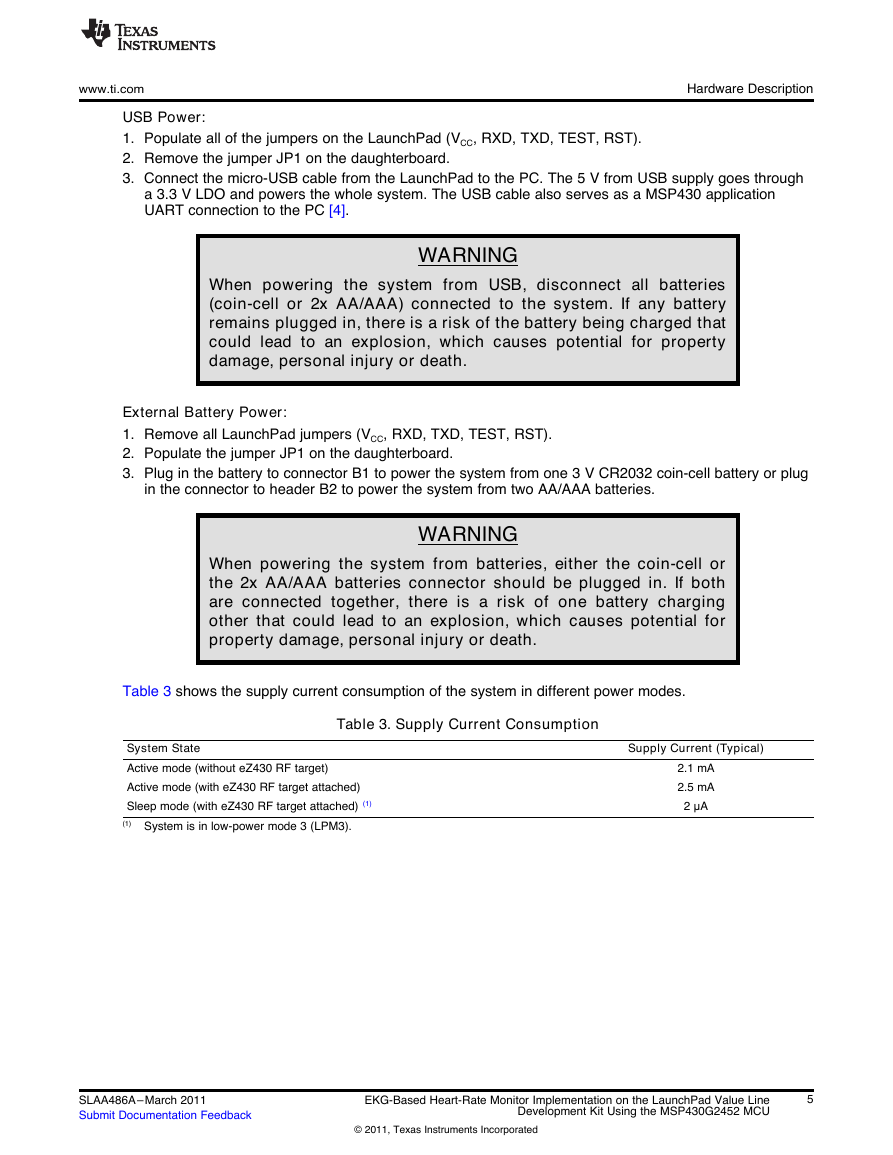
Table 3 shows the supply current consumption of the system in different power modes.
Table 3. Supply Current Consumption
System State
Active mode (without eZ430 RF target)
Active mode (with eZ430 RF target attached)
Sleep mode (with eZ430 RF target attached) (1)
(1) System is in low-power mode 3 (LPM3).
Supply Current (Typical)
2.1 mA
2.5 mA
2 μA
SLAA486A–March 2011
Submit Documentation Feedback
EKG-Based Heart-Rate Monitor Implementation on the LaunchPad Value Line
Development Kit Using the MSP430G2452 MCU
5
© 2011, Texas Instruments Incorporated
�
Software
www.ti.com
3
Software
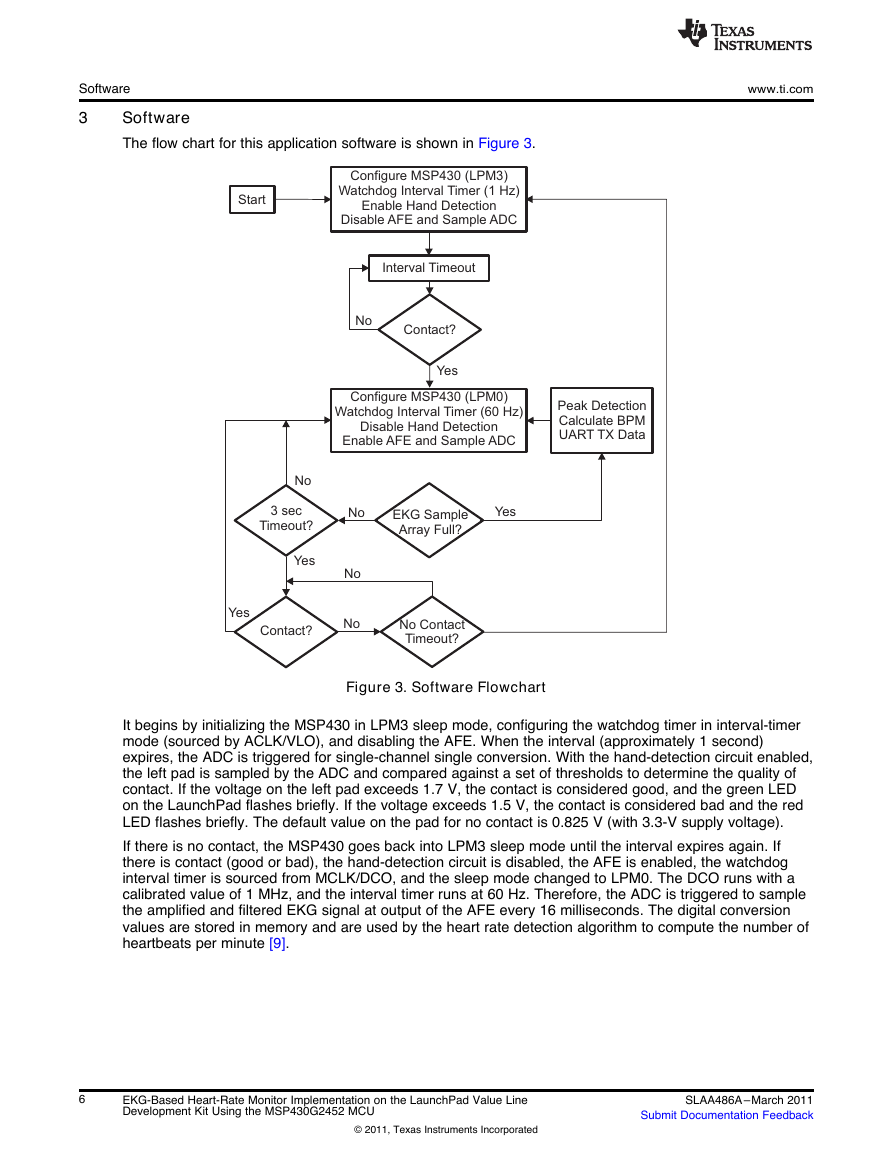
The flow chart for this application software is shown in Figure 3.
Figure 3. Software Flowchart
It begins by initializing the MSP430 in LPM3 sleep mode, configuring the watchdog timer in interval-timer
mode (sourced by ACLK/VLO), and disabling the AFE. When the interval (approximately 1 second)
expires, the ADC is triggered for single-channel single conversion. With the hand-detection circuit enabled,
the left pad is sampled by the ADC and compared against a set of thresholds to determine the quality of
contact. If the voltage on the left pad exceeds 1.7 V, the contact is considered good, and the green LED
on the LaunchPad flashes briefly. If the voltage exceeds 1.5 V, the contact is considered bad and the red
LED flashes briefly. The default value on the pad for no contact is 0.825 V (with 3.3-V supply voltage).
If there is no contact, the MSP430 goes back into LPM3 sleep mode until the interval expires again. If
there is contact (good or bad), the hand-detection circuit is disabled, the AFE is enabled, the watchdog
interval timer is sourced from MCLK/DCO, and the sleep mode changed to LPM0. The DCO runs with a
calibrated value of 1 MHz, and the interval timer runs at 60 Hz. Therefore, the ADC is triggered to sample
the amplified and filtered EKG signal at output of the AFE every 16 milliseconds. The digital conversion
values are stored in memory and are used by the heart rate detection algorithm to compute the number of
heartbeats per minute [9].
6
EKG-Based Heart-Rate Monitor Implementation on the LaunchPad Value Line
Development Kit Using the MSP430G2452 MCU
SLAA486A–March 2011
Submit Documentation Feedback
© 2011, Texas Instruments Incorporated
StartConfigure MSP430 (LPM3)Watchdog IntervalTimer (1 Hz)Enable Hand DetectionDisableAFE and SampleADCIntervalTimeoutContact?YesNoConfigure MSP430 (LPM0)Watchdog IntervalTimer (60 Hz)Disable Hand DetectionEnableAFE and SampleADCPeak DetectionCalculate BPMUARTTX DataYesNoNoEKG SampleArray Full?No ContactTimeout?NoNoYesContact?Yes3 secTimeout?�
www.ti.com
References
The heart rate value is transmitted via a Timer-A based UART [10]. The UART output can be relayed to
the PC by means of either the back-channel UART-over-USB connection on the LaunchPad or the eZ430
RF target header on the daughterboard. During the EKG sampling by the ADC, the hand-detection circuit
is momentarily enabled every three seconds to ensure that contact is being made. If there is contact, the
application goes back to EKG sampling. If not, the hand-detection circuit remains enabled, and the
applications keeping checking for contact for approximately 10 seconds. If there is still no contact, the AFE
is disabled and the MSP430 returns back to the initial LPM3 state where it checks for contact every
second.
Details on programming the software on the heart-rate monitor setup are provided in Appendix B and the
eZ430 RF target boards in Appendix C. Figure 4 shows the complete hardware setup in action (left side)
and the UART output log display on the HyperTerminal application window on the PC (right side).
Figure 4. Heart-Rate Monitor Setup (left) and UART Output on PC (right)
4
References
1. http://www.daviddarling.info/images/sinoatrial_node.jpg
2. http://www.medterms.com
3. Heart-Rate and EKG Monitor Using the MSP430FG439 (SLAA280)
4. MSP-EXP430G2 LaunchPad Experimenter Board User’s Guide (SLAU318)
5. eZ430-RF2500 Development Tool User’s Guide (SLAU227)
6. A2500R24A-EZ4x - Integrated Radio (AIR) EZ4x Module Series Product Brief: Anaren
(http://www.anaren.com)
7. AMB8423-EM – 868 MHz Radio Module for TI Development Tool eZ430-RF2500 Datasheet: Amber
Wireless (http://www.amber-wireless.de/index.php)
8. Wireless Sensor Monitor Using the eZ430-RF2500 (SLAA378)
9. Sourabh Ravindran, Steven Dunbar, and Bhargavi Nisarga, Real-Time, Low-Complexity, Low Memory
Solution to ECG-Based Heart Rate Detection, IEEE Engineering in Medicine and Biology Society
(EMBC), 2009.(http://ieeexplore.ieee.org/stamp/stamp.jsp?arnumber=05334447)
10. Implementing a UART Function With TimerA3 (SLAA078)
11. MSP430G2x52, MSP430Gx12 Mixed Signal Microcontroller Datasheet (SLAS722)
SLAA486A–March 2011
Submit Documentation Feedback
EKG-Based Heart-Rate Monitor Implementation on the LaunchPad Value Line
Development Kit Using the MSP430G2452 MCU
7
© 2011, Texas Instruments Incorporated
�
Appendix A Amplifier Options
www.ti.com
A.1
Instrumentation Amplifier Options
This reference design uses the INA332 as the instrumentation amplifier for the analog front end. Table 4
shows other options for the instrumentation amplifier.
Device Name
INA321
INA332
INA333
Table 4. Instrumentation Amplifier Comparison
Quiescent current
Shutdown current
Bandwidth
Slew rate
Supply voltage
Price/1ku
(listed on
http://www.ti.com)
40 µA/channel
< 1 μA
500 kHz, G = 5 V/V
500 kHz, G = 5 V/V
2.7 V – 5.5 V
490 μA/channel
~ 0.01 μA
2 MHz, G = 25
5 V/μs for G = 25
2.7 V – 5.5 V
50 μA/channel
No shutdown
35 kHz, G = 10
0.16 V/μs for G = 1
1.8 V – 5.5 V
1.25
0.55
1.80
The INA321 is pin-to-pin compatible with the INA332 and uses a two-resistor feedback network to set the
gain. It also offers significantly lower quiescent current, although it costs more. The INA333 has a different
architecture in which the gain is set by one resistor. While it lacks a shutdown pin, the quiescent current
consumption levels are comparable to the INA321 with the advantage of operating as low as 1.8 V. While
the most expensive of the three, the INA333 is ideal for battery-operated portable systems with
low-voltage operating range.
8
EKG-Based Heart-Rate Monitor Implementation on the LaunchPad Value Line
Development Kit Using the MSP430G2452 MCU
SLAA486A–March 2011
Submit Documentation Feedback
© 2011, Texas Instruments Incorporated
A1–+A2–+A3–+R1R2RGVREF40kΩ10kΩ10kΩV+INV–INV+V–ShutdownVOUTINA332G = 5 + 5(R/R)2140kΩREFVIN–160kΩVIN+40kΩA1–+40kΩ160kΩR1RGR2VOUTA2–+A3–+Gain = 5 + 5(R2/R1)V= (V–V)•GainOUTIN+IN–V+V–ShutdownA1–+A3–+–A2+–RFI Filtered InputsRFI Filtered InputsRFI Filtered InputsRFI Filtered InputsINA333RGVIN–VIN+2183V–4V+76VOUT5REF50kΩ50kΩ150kΩ150kΩ150kΩ150kΩG = 1 +100kΩRG�






 2023年江西萍乡中考道德与法治真题及答案.doc
 2012年重庆南川中考生物真题及答案.doc
 2013年江西师范大学地理学综合及文艺理论基础考研真题.doc
 2020年四川甘孜小升初语文真题及答案I卷.doc
 2020年注册岩土工程师专业基础考试真题及答案.doc
 2023-2024学年福建省厦门市九年级上学期数学月考试题及答案.doc
 2021-2022学年辽宁省沈阳市大东区九年级上学期语文期末试题及答案.doc
 2022-2023学年北京东城区初三第一学期物理期末试卷及答案.doc
 2018上半年江西教师资格初中地理学科知识与教学能力真题及答案.doc
 2012年河北国家公务员申论考试真题及答案-省级.doc
 2020-2021学年江苏省扬州市江都区邵樊片九年级上学期数学第一次质量检测试题及答案.doc
 2022下半年黑龙江教师资格证中学综合素质真题及答案.doc