1 Overview of the manual
Table 1. Sections related to each STM32F10xxx product
Table 2. Sections related to each peripheral
2 Documentation conventions
2.1 List of abbreviations for registers
2.2 Glossary
2.3 Peripheral availability
3 Memory and bus architecture
3.1 System architecture
ICode bus
DCode bus
System bus
DMA bus
BusMatrix
AHB/APB bridges (APB)
3.2 Memory organization
3.3 Memory map
Table 3. Register boundary addresses
3.3.1 Embedded SRAM
3.3.2 Bit banding
3.3.3 Embedded Flash memory
Table 4. Flash module organization (low-density devices)
Table 5. Flash module organization (medium-density devices)
Table 6. Flash module organization (high-density devices)
Table 7. Flash module organization (connectivity line devices)
Table 8. XL-density Flash module organization
Reading the Flash memory
Programming and erasing the Flash memory
Flash access control register (FLASH_ACR)
3.4 Boot configuration
Table 9. Boot modes
Embedded boot loader
4 CRC calculation unit
4.1 CRC introduction
4.2 CRC main features
4.3 CRC functional description
4.4 CRC registers
4.4.1 Data register (CRC_DR)
4.4.2 Independent data register (CRC_IDR)
4.4.3 Control register (CRC_CR)
4.4.4 CRC register map
Table 10. CRC calculation unit register map and reset values
5 Power control (PWR)
5.1 Power supplies
5.1.1 Independent A/D and D/A converter supply and reference voltage
On 100-pin and 144-pin packages
On 64-pin packages and packages with less pins
5.1.2 Battery backup domain
5.1.3 Voltage regulator
5.2 Power supply supervisor
5.2.1 Power on reset (POR)/power down reset (PDR)
5.2.2 Programmable voltage detector (PVD)
5.3 Low-power modes
Table 11. Low-power mode summary
5.3.1 Slowing down system clocks
5.3.2 Peripheral clock gating
5.3.3 Sleep mode
Entering Sleep mode
Exiting Sleep mode
Table 12. Sleep-now
Table 13. Sleep-on-exit
5.3.4 Stop mode
Entering Stop mode
Table 14. Stop mode
5.3.5 Standby mode
Entering Standby mode
Exiting Standby mode
Table 15. Standby mode
I/O states in Standby mode
Debug mode
5.3.6 Auto-wakeup (AWU) from low-power mode
5.4 Power control registers
5.4.1 Power control register (PWR_CR)
5.4.2 Power control/status register (PWR_CSR)
5.4.3 PWR register map
Table 16. PWR register map and reset values
6 Backup registers (BKP)
6.1 BKP introduction
6.2 BKP main features
6.3 BKP functional description
6.3.1 Tamper detection
6.3.2 RTC calibration
6.4 BKP registers
6.4.1 Backup data register x (BKP_DRx) (x = 1 ..42)
6.4.2 RTC clock calibration register (BKP_RTCCR)
6.4.3 Backup control register (BKP_CR)
6.4.4 Backup control/status register (BKP_CSR)
6.4.5 BKP register map
Table 17. BKP register map and reset values
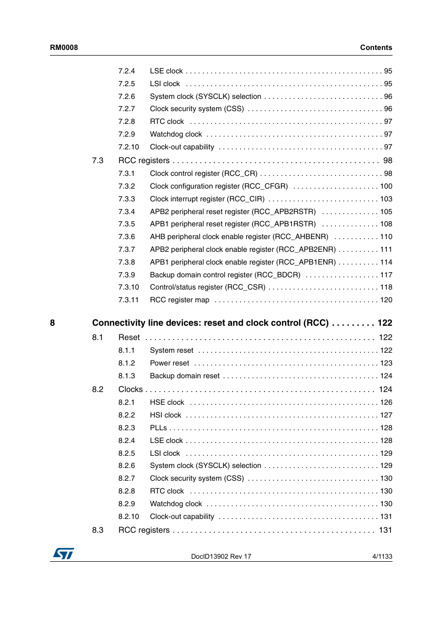
7 Low-, medium-, high- and XL-density reset and clock control (RCC)
7.1 Reset
7.1.1 System reset
Software reset
Low-power management reset
7.1.2 Power reset
7.1.3 Backup domain reset
7.2 Clocks
7.2.1 HSE clock
External source (HSE bypass)
External crystal/ceramic resonator (HSE crystal)
7.2.2 HSI clock
Calibration
7.2.3 PLL
7.2.4 LSE clock
External source (LSE bypass)
7.2.5 LSI clock
LSI calibration
7.2.6 System clock (SYSCLK) selection
7.2.7 Clock security system (CSS)
7.2.8 RTC clock
7.2.9 Watchdog clock
7.2.10 Clock-out capability
7.3 RCC registers
7.3.1 Clock control register (RCC_CR)
7.3.2 Clock configuration register (RCC_CFGR)
7.3.3 Clock interrupt register (RCC_CIR)
7.3.4 APB2 peripheral reset register (RCC_APB2RSTR)
7.3.5 APB1 peripheral reset register (RCC_APB1RSTR)
7.3.6 AHB peripheral clock enable register (RCC_AHBENR)
7.3.7 APB2 peripheral clock enable register (RCC_APB2ENR)
7.3.8 APB1 peripheral clock enable register (RCC_APB1ENR)
7.3.9 Backup domain control register (RCC_BDCR)
7.3.10 Control/status register (RCC_CSR)
7.3.11 RCC register map
Table 18. RCC register map and reset values
8 Connectivity line devices: reset and clock control (RCC)
8.1 Reset
8.1.1 System reset
Software reset
Low-power management reset
8.1.2 Power reset
8.1.3 Backup domain reset
8.2 Clocks
8.2.1 HSE clock
External source (HSE bypass)
External crystal/ceramic resonator (HSE crystal)
8.2.2 HSI clock
Calibration
8.2.3 PLLs
8.2.4 LSE clock
External source (LSE bypass)
8.2.5 LSI clock
LSI calibration
8.2.6 System clock (SYSCLK) selection
8.2.7 Clock security system (CSS)
8.2.8 RTC clock
8.2.9 Watchdog clock
8.2.10 Clock-out capability
8.3 RCC registers
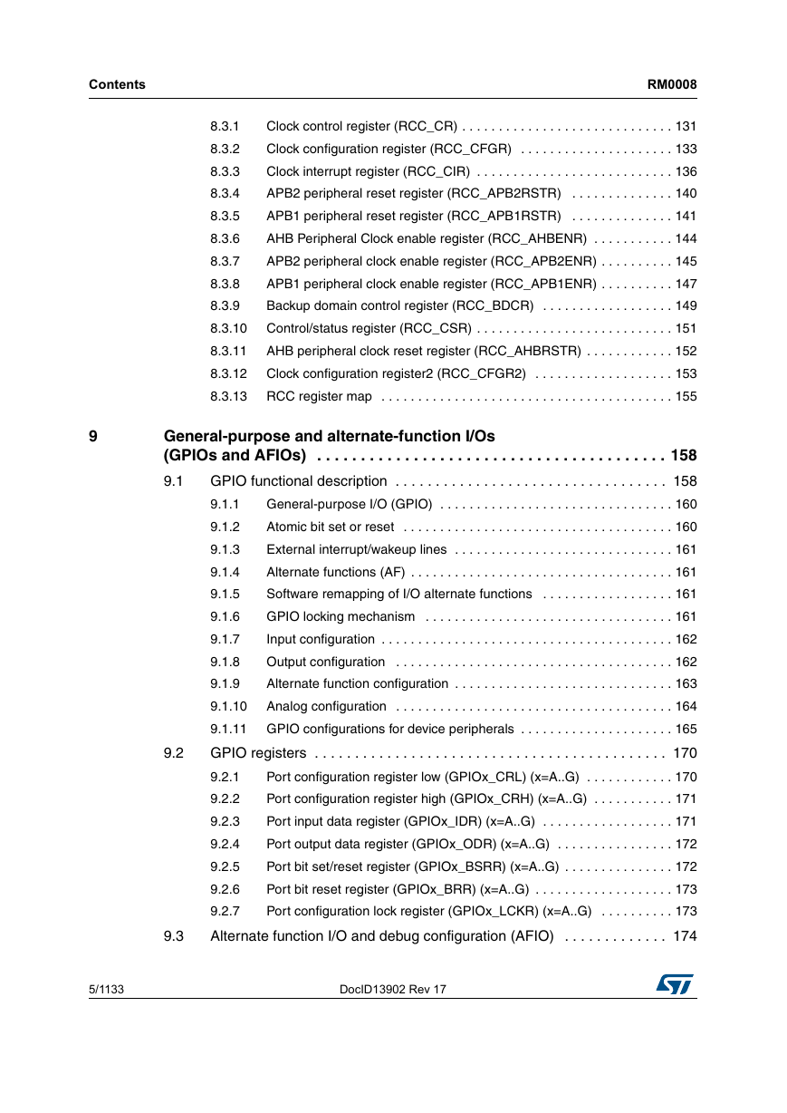
8.3.1 Clock control register (RCC_CR)
8.3.2 Clock configuration register (RCC_CFGR)
8.3.3 Clock interrupt register (RCC_CIR)
8.3.4 APB2 peripheral reset register (RCC_APB2RSTR)
8.3.5 APB1 peripheral reset register (RCC_APB1RSTR)
8.3.6 AHB Peripheral Clock enable register (RCC_AHBENR)
8.3.7 APB2 peripheral clock enable register (RCC_APB2ENR)
8.3.8 APB1 peripheral clock enable register (RCC_APB1ENR)
8.3.9 Backup domain control register (RCC_BDCR)
8.3.10 Control/status register (RCC_CSR)
8.3.11 AHB peripheral clock reset register (RCC_AHBRSTR)
8.3.12 Clock configuration register2 (RCC_CFGR2)
8.3.13 RCC register map
Table 19. RCC register map and reset values
9 General-purpose and alternate-function I/Os (GPIOs and AFIOs)
9.1 GPIO functional description
Table 20. Port bit configuration table
Table 21. Output MODE bits
9.1.1 General-purpose I/O (GPIO)
9.1.2 Atomic bit set or reset
9.1.3 External interrupt/wakeup lines
9.1.4 Alternate functions (AF)
9.1.5 Software remapping of I/O alternate functions
9.1.6 GPIO locking mechanism
9.1.7 Input configuration
9.1.8 Output configuration
9.1.9 Alternate function configuration
9.1.10 Analog configuration
9.1.11 GPIO configurations for device peripherals
Table 22. Advanced timers TIM1 and TIM8
Table 23. General-purpose timers TIM2/3/4/5
Table 24. USARTs
Table 25. SPI
Table 26. I2S
Table 27. I2C
Table 28. BxCAN
Table 29. USB
Table 30. OTG_FS pin configuration
Table 31. SDIO
Table 32. FSMC
Table 33. Other IOs
9.2 GPIO registers
9.2.1 Port configuration register low (GPIOx_CRL) (x=A..G)
9.2.2 Port configuration register high (GPIOx_CRH) (x=A..G)
9.2.3 Port input data register (GPIOx_IDR) (x=A..G)
9.2.4 Port output data register (GPIOx_ODR) (x=A..G)
9.2.5 Port bit set/reset register (GPIOx_BSRR) (x=A..G)
9.2.6 Port bit reset register (GPIOx_BRR) (x=A..G)
9.2.7 Port configuration lock register (GPIOx_LCKR) (x=A..G)
9.3 Alternate function I/O and debug configuration (AFIO)
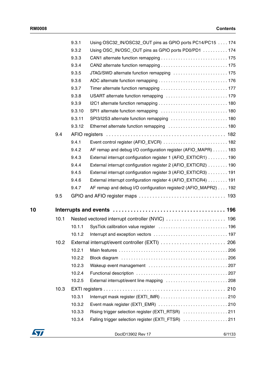
9.3.1 Using OSC32_IN/OSC32_OUT pins as GPIO ports PC14/PC15
9.3.2 Using OSC_IN/OSC_OUT pins as GPIO ports PD0/PD1
9.3.3 CAN1 alternate function remapping
Table 34. CAN1 alternate function remapping
9.3.4 CAN2 alternate function remapping
Table 35. CAN2 alternate function remapping
9.3.5 JTAG/SWD alternate function remapping
Table 36. Debug interface signals
Table 37. Debug port mapping
9.3.6 ADC alternate function remapping
Table 38. ADC1 external trigger injected conversion alternate function remapping
Table 39. ADC1 external trigger regular conversion alternate function remapping
Table 40. ADC2 external trigger injected conversion alternate function remapping
Table 41. ADC2 external trigger regular conversion alternate function remapping
9.3.7 Timer alternate function remapping
Table 42. TIM5 alternate function remapping
Table 43. TIM4 alternate function remapping
Table 44. TIM3 alternate function remapping
Table 45. TIM2 alternate function remapping
Table 46. TIM1 alternate function remapping
Table 47. TIM9 remapping
Table 48. TIM10 remapping
Table 49. TIM11 remapping
Table 50. TIM13 remapping
Table 51. TIM14 remapping
9.3.8 USART alternate function remapping
Table 52. USART3 remapping
Table 53. USART2 remapping
Table 54. USART1 remapping
9.3.9 I2C1 alternate function remapping
Table 55. I2C1 remapping
9.3.10 SPI1 alternate function remapping
Table 56. SPI1 remapping
9.3.11 SPI3/I2S3 alternate function remapping
Table 57. SPI3/I2S3 remapping
9.3.12 Ethernet alternate function remapping
Table 58. ETH remapping
9.4 AFIO registers
9.4.1 Event control register (AFIO_EVCR)
9.4.2 AF remap and debug I/O configuration register (AFIO_MAPR)
Memory map and bit definitions for low-, medium- high- and XL-density devices:
Memory map and bit definitions for connectivity line devices:
9.4.3 External interrupt configuration register 1 (AFIO_EXTICR1)
9.4.4 External interrupt configuration register 2 (AFIO_EXTICR2)
9.4.5 External interrupt configuration register 3 (AFIO_EXTICR3)
9.4.6 External interrupt configuration register 4 (AFIO_EXTICR4)
9.4.7 AF remap and debug I/O configuration register2 (AFIO_MAPR2)
9.5 GPIO and AFIO register maps
Table 59. GPIO register map and reset values
Table 60. AFIO register map and reset values
10 Interrupts and events
10.1 Nested vectored interrupt controller (NVIC)
Features
10.1.1 SysTick calibration value register
10.1.2 Interrupt and exception vectors
Table 61. Vector table for connectivity line devices
Table 62. Vector table for XL-density devices
Table 63. Vector table for other STM32F10xxx devices
10.2 External interrupt/event controller (EXTI)
10.2.1 Main features
10.2.2 Block diagram
10.2.3 Wakeup event management
10.2.4 Functional description
Hardware interrupt selection
Hardware event selection
Software interrupt/event selection
10.2.5 External interrupt/event line mapping
10.3 EXTI registers
10.3.1 Interrupt mask register (EXTI_IMR)
10.3.2 Event mask register (EXTI_EMR)
10.3.3 Rising trigger selection register (EXTI_RTSR)
10.3.4 Falling trigger selection register (EXTI_FTSR)
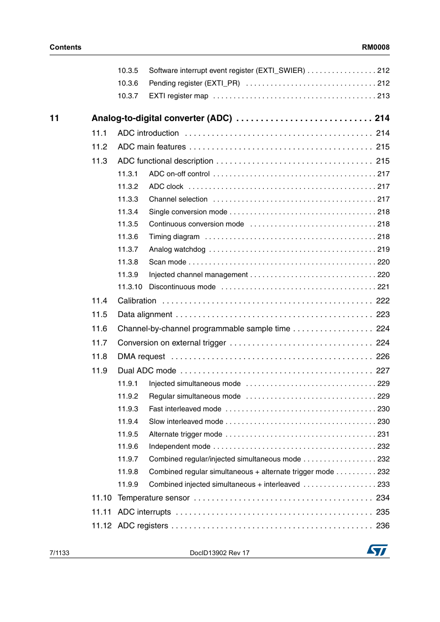
10.3.5 Software interrupt event register (EXTI_SWIER)
10.3.6 Pending register (EXTI_PR)
10.3.7 EXTI register map
Table 64. External interrupt/event controller register map and reset values
11 Analog-to-digital converter (ADC)
11.1 ADC introduction
11.2 ADC main features
11.3 ADC functional description
Table 65. ADC pins
11.3.1 ADC on-off control
11.3.2 ADC clock
11.3.3 Channel selection
Temperature sensor/VREFINT internal channels
11.3.4 Single conversion mode
11.3.5 Continuous conversion mode
11.3.6 Timing diagram
11.3.7 Analog watchdog
Table 66. Analog watchdog channel selection
11.3.8 Scan mode
11.3.9 Injected channel management
Triggered injection
Auto-injection
11.3.10 Discontinuous mode
Regular group
Injected group
11.4 Calibration
11.5 Data alignment
11.6 Channel-by-channel programmable sample time
11.7 Conversion on external trigger
Table 67. External trigger for regular channels for ADC1 and ADC2
Table 68. External trigger for injected channels for ADC1 and ADC2
Table 69. External trigger for regular channels for ADC3
Table 70. External trigger for injected channels for ADC3
11.8 DMA request
11.9 Dual ADC mode
11.9.1 Injected simultaneous mode
11.9.2 Regular simultaneous mode
11.9.3 Fast interleaved mode
11.9.4 Slow interleaved mode
11.9.5 Alternate trigger mode
11.9.6 Independent mode
11.9.7 Combined regular/injected simultaneous mode
11.9.8 Combined regular simultaneous + alternate trigger mode
11.9.9 Combined injected simultaneous + interleaved
11.10 Temperature sensor
Reading the temperature
11.11 ADC interrupts
Table 71. ADC interrupts
11.12 ADC registers
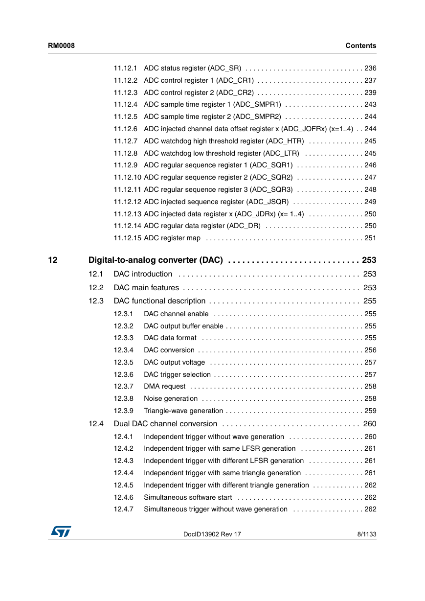
11.12.1 ADC status register (ADC_SR)
11.12.2 ADC control register 1 (ADC_CR1)
11.12.3 ADC control register 2 (ADC_CR2)
11.12.4 ADC sample time register 1 (ADC_SMPR1)
11.12.5 ADC sample time register 2 (ADC_SMPR2)
11.12.6 ADC injected channel data offset register x (ADC_JOFRx) (x=1..4)
11.12.7 ADC watchdog high threshold register (ADC_HTR)
11.12.8 ADC watchdog low threshold register (ADC_LTR)
11.12.9 ADC regular sequence register 1 (ADC_SQR1)
11.12.10 ADC regular sequence register 2 (ADC_SQR2)
11.12.11 ADC regular sequence register 3 (ADC_SQR3)
11.12.12 ADC injected sequence register (ADC_JSQR)
11.12.13 ADC injected data register x (ADC_JDRx) (x= 1..4)
11.12.14 ADC regular data register (ADC_DR)
11.12.15 ADC register map
Table 72. ADC register map and reset values
12 Digital-to-analog converter (DAC)
12.1 DAC introduction
12.2 DAC main features
Table 73. DAC pins
12.3 DAC functional description
12.3.1 DAC channel enable
12.3.2 DAC output buffer enable
12.3.3 DAC data format
12.3.4 DAC conversion
12.3.5 DAC output voltage
12.3.6 DAC trigger selection
Table 74. External triggers
12.3.7 DMA request
12.3.8 Noise generation
12.3.9 Triangle-wave generation
12.4 Dual DAC channel conversion
12.4.1 Independent trigger without wave generation
12.4.2 Independent trigger with same LFSR generation
12.4.3 Independent trigger with different LFSR generation
12.4.4 Independent trigger with same triangle generation
12.4.5 Independent trigger with different triangle generation
12.4.6 Simultaneous software start
12.4.7 Simultaneous trigger without wave generation
12.4.8 Simultaneous trigger with same LFSR generation
12.4.9 Simultaneous trigger with different LFSR generation
12.4.10 Simultaneous trigger with same triangle generation
12.4.11 Simultaneous trigger with different triangle generation
12.5 DAC registers
12.5.1 DAC control register (DAC_CR)
12.5.2 DAC software trigger register (DAC_SWTRIGR)
12.5.3 DAC channel1 12-bit right-aligned data holding register (DAC_DHR12R1)
12.5.4 DAC channel1 12-bit left aligned data holding register (DAC_DHR12L1)
12.5.5 DAC channel1 8-bit right aligned data holding register (DAC_DHR8R1)
12.5.6 DAC channel2 12-bit right aligned data holding register (DAC_DHR12R2)
12.5.7 DAC channel2 12-bit left aligned data holding register (DAC_DHR12L2)
12.5.8 DAC channel2 8-bit right-aligned data holding register (DAC_DHR8R2)
12.5.9 Dual DAC 12-bit right-aligned data holding register (DAC_DHR12RD)
12.5.10 DUAL DAC 12-bit left aligned data holding register (DAC_DHR12LD)
12.5.11 DUAL DAC 8-bit right aligned data holding register (DAC_DHR8RD)
12.5.12 DAC channel1 data output register (DAC_DOR1)
12.5.13 DAC channel2 data output register (DAC_DOR2)
12.5.14 DAC register map
Table 75. DAC register map
13 Direct memory access controller (DMA)
13.1 DMA introduction
13.2 DMA main features
13.3 DMA functional description
13.3.1 DMA transactions
13.3.2 Arbiter
13.3.3 DMA channels
Programmable data sizes
Pointer incrementation
Channel configuration procedure
Circular mode
Memory-to-memory mode
13.3.4 Programmable data width, data alignment and endians
Table 76. Programmable data width and endian behavior (when bits PINC = MINC = 1)
Addressing an AHB peripheral that does not support byte or halfword write operations
13.3.5 Error management
13.3.6 Interrupts
Table 77. DMA interrupt requests
13.3.7 DMA request mapping
DMA1 controller
Table 78. Summary of DMA1 requests for each channel
DMA2 controller
Table 79. Summary of DMA2 requests for each channel
13.4 DMA registers
13.4.1 DMA interrupt status register (DMA_ISR)
13.4.2 DMA interrupt flag clear register (DMA_IFCR)
13.4.3 DMA channel x configuration register (DMA_CCRx) (x = 1..7, where x = channel number)
13.4.4 DMA channel x number of data register (DMA_CNDTRx) (x = 1..7, where x = channel number)
13.4.5 DMA channel x peripheral address register (DMA_CPARx) (x = 1..7, where x = channel number)
13.4.6 DMA channel x memory address register (DMA_CMARx) (x = 1..7, where x = channel number)
13.4.7 DMA register map
Table 80. DMA register map and reset values
14 Advanced-control timers (TIM1 and TIM8)
14.1 TIM1 and TIM8 introduction
14.2 TIM1 and TIM8 main features
14.3 TIM1 and TIM8 functional description
14.3.1 Time-base unit
Prescaler description
14.3.2 Counter modes
Upcounting mode
Downcounting mode
Center-aligned mode (up/down counting)
14.3.3 Repetition counter
14.3.4 Clock selection
Internal clock source (CK_INT)
External clock source mode 1
External clock source mode 2
14.3.5 Capture/compare channels
14.3.6 Input capture mode
14.3.7 PWM input mode
14.3.8 Forced output mode
14.3.9 Output compare mode
14.3.10 PWM mode
PWM edge-aligned mode
PWM center-aligned mode
14.3.11 Complementary outputs and dead-time insertion
Re-directing OCxREF to OCx or OCxN
14.3.12 Using the break function
14.3.13 Clearing the OCxREF signal on an external event
14.3.14 6-step PWM generation
14.3.15 One-pulse mode
14.3.16 Encoder interface mode
Table 81. Counting direction versus encoder signals
14.3.17 Timer input XOR function
14.3.18 Interfacing with Hall sensors
14.3.19 TIMx and external trigger synchronization
Slave mode: Reset mode
Slave mode: Gated mode
Slave mode: Trigger mode
Slave mode: external clock mode 2 + trigger mode
14.3.20 Timer synchronization
14.3.21 Debug mode
14.4 TIM1 and TIM8 registers
14.4.1 TIM1 and TIM8 control register 1 (TIMx_CR1)
14.4.2 TIM1 and TIM8 control register 2 (TIMx_CR2)
14.4.3 TIM1 and TIM8 slave mode control register (TIMx_SMCR)
Table 82. TIMx Internal trigger connection
14.4.4 TIM1 and TIM8 DMA/interrupt enable register (TIMx_DIER)
14.4.5 TIM1 and TIM8 status register (TIMx_SR)
14.4.6 TIM1 and TIM8 event generation register (TIMx_EGR)
14.4.7 TIM1 and TIM8 capture/compare mode register 1 (TIMx_CCMR1)
Output compare mode:
Input capture mode
14.4.8 TIM1 and TIM8 capture/compare mode register 2 (TIMx_CCMR2)
Output compare mode
Input capture mode
14.4.9 TIM1 and TIM8 capture/compare enable register (TIMx_CCER)
Table 83. Output control bits for complementary OCx and OCxN channels with break feature
14.4.10 TIM1 and TIM8 counter (TIMx_CNT)
14.4.11 TIM1 and TIM8 prescaler (TIMx_PSC)
14.4.12 TIM1 and TIM8 auto-reload register (TIMx_ARR)
14.4.13 TIM1 and TIM8 repetition counter register (TIMx_RCR)
14.4.14 TIM1 and TIM8 capture/compare register 1 (TIMx_CCR1)
14.4.15 TIM1 and TIM8 capture/compare register 2 (TIMx_CCR2)
14.4.16 TIM1 and TIM8 capture/compare register 3 (TIMx_CCR3)
14.4.17 TIM1 and TIM8 capture/compare register 4 (TIMx_CCR4)
14.4.18 TIM1 and TIM8 break and dead-time register (TIMx_BDTR)
14.4.19 TIM1 and TIM8 DMA control register (TIMx_DCR)
14.4.20 TIM1 and TIM8 DMA address for full transfer (TIMx_DMAR)
Example of how to use the DMA burst feature
14.4.21 TIM1 and TIM8 register map
Table 84. TIM1 and TIM8 register map and reset values
15 General-purpose timers (TIM2 to TIM5)
15.1 TIM2 to TIM5 introduction
15.2 TIMx main features
15.3 TIMx functional description
15.3.1 Time-base unit
Prescaler description
15.3.2 Counter modes
Upcounting mode
Downcounting mode
Center-aligned mode (up/down counting)
15.3.3 Clock selection
Internal clock source (CK_INT)
External clock source mode 1
External clock source mode 2
15.3.4 Capture/compare channels
15.3.5 Input capture mode
15.3.6 PWM input mode
15.3.7 Forced output mode
15.3.8 Output compare mode
15.3.9 PWM mode
PWM edge-aligned mode
Upcounting configuration
Downcounting configuration
PWM center-aligned mode
15.3.10 One-pulse mode
Particular case: OCx fast enable:
15.3.11 Clearing the OCxREF signal on an external event
15.3.12 Encoder interface mode
Table 85. Counting direction versus encoder signals
15.3.13 Timer input XOR function
15.3.14 Timers and external trigger synchronization
Slave mode: Reset mode
Slave mode: Gated mode
Slave mode: Trigger mode
Slave mode: External Clock mode 2 + trigger mode
15.3.15 Timer synchronization
Using one timer as prescaler for another timer
Using one timer to enable another timer
Using one timer to start another timer
Starting 2 timers synchronously in response to an external trigger
15.3.16 Debug mode
15.4 TIMx2 to TIM5 registers
15.4.1 TIMx control register 1 (TIMx_CR1)
15.4.2 TIMx control register 2 (TIMx_CR2)
15.4.3 TIMx slave mode control register (TIMx_SMCR)
Table 86. TIMx Internal trigger connection
15.4.4 TIMx DMA/Interrupt enable register (TIMx_DIER)
15.4.5 TIMx status register (TIMx_SR)
15.4.6 TIMx event generation register (TIMx_EGR)
15.4.7 TIMx capture/compare mode register 1 (TIMx_CCMR1)
Output compare mode
Input capture mode
15.4.8 TIMx capture/compare mode register 2 (TIMx_CCMR2)
Output compare mode
Input capture mode
15.4.9 TIMx capture/compare enable register (TIMx_CCER)
Table 87. Output control bit for standard OCx channels
15.4.10 TIMx counter (TIMx_CNT)
15.4.11 TIMx prescaler (TIMx_PSC)
15.4.12 TIMx auto-reload register (TIMx_ARR)
15.4.13 TIMx capture/compare register 1 (TIMx_CCR1)
15.4.14 TIMx capture/compare register 2 (TIMx_CCR2)
15.4.15 TIMx capture/compare register 3 (TIMx_CCR3)
15.4.16 TIMx capture/compare register 4 (TIMx_CCR4)
15.4.17 TIMx DMA control register (TIMx_DCR)
15.4.18 TIMx DMA address for full transfer (TIMx_DMAR)
Example of how to use the DMA burst feature
15.4.19 TIMx register map
Table 88. TIMx register map and reset values
16 General-purpose timers (TIM9 to TIM14)
16.1 TIM9 to TIM14 introduction
16.2 TIM9 to TIM14 main features
16.2.1 TIM9/TIM12 main features
16.2.2 TIM10/TIM11 and TIM13/TIM14 main features
16.3 TIM9 to TIM14 functional description
16.3.1 Time-base unit
Prescaler description
16.3.2 Counter modes
Upcounting mode
16.3.3 Clock selection
Internal clock source (CK_INT)
External clock source mode 1(TIM9 and TIM12)
16.3.4 Capture/compare channels
16.3.5 Input capture mode
16.3.6 PWM input mode (only for TIM9/12)
16.3.7 Forced output mode
16.3.8 Output compare mode
16.3.9 PWM mode
PWM edge-aligned mode
16.3.10 One-pulse mode
16.3.11 TIM9/12 external trigger synchronization
Slave mode: Reset mode
Slave mode: Gated mode
Slave mode: Trigger mode
16.3.12 Timer synchronization (TIM9/12)
16.3.13 Debug mode
16.4 TIM9 and TIM12 registers
16.4.1 TIM9/12 control register 1 (TIMx_CR1)
16.4.2 TIM9/12 slave mode control register (TIMx_SMCR)
Table 89. TIMx internal trigger connection
16.4.3 TIM9/12 Interrupt enable register (TIMx_DIER)
16.4.4 TIM9/12 status register (TIMx_SR)
16.4.5 TIM9/12 event generation register (TIMx_EGR)
16.4.6 TIM9/12 capture/compare mode register 1 (TIMx_CCMR1)
Output compare mode
Input capture mode
16.4.7 TIM9/12 capture/compare enable register (TIMx_CCER)
Table 90. Output control bit for standard OCx channels
16.4.8 TIM9/12 counter (TIMx_CNT)
16.4.9 TIM9/12 prescaler (TIMx_PSC)
16.4.10 TIM9/12 auto-reload register (TIMx_ARR)
16.4.11 TIM9/12 capture/compare register 1 (TIMx_CCR1)
16.4.12 TIM9/12 capture/compare register 2 (TIMx_CCR2)
16.4.13 TIM9/12 register map
Table 91. TIM9/12 register map and reset values
16.5 TIM10/11/13/14 registers
16.5.1 TIM10/11/13/14 control register 1 (TIMx_CR1)
16.5.2 TIM10/11/13/14 Interrupt enable register (TIMx_DIER)
16.5.3 TIM10/11/13/14 status register (TIMx_SR)
16.5.4 TIM10/11/13/14 event generation register (TIMx_EGR)
16.5.5 TIM10/11/13/14 capture/compare mode register 1 (TIMx_CCMR1)
Output compare mode
Input capture mode
16.5.6 TIM10/11/13/14 capture/compare enable register (TIMx_CCER)
Table 92. Output control bit for standard OCx channels
16.5.7 TIM10/11/13/14 counter (TIMx_CNT)
16.5.8 TIM10/11/13/14 prescaler (TIMx_PSC)
16.5.9 TIM10/11/13/14 auto-reload register (TIMx_ARR)
16.5.10 TIM10/11/13/14 capture/compare register 1 (TIMx_CCR1)
16.5.11 TIM10/11/13/14 register map
Table 93. TIM10/11/13/14 register map and reset values
17 Basic timers (TIM6 and TIM7)
17.1 TIM6 and TIM7 introduction
17.2 TIM6 and TIM7 main features
17.3 TIM6 and TIM7 functional description
17.3.1 Time-base unit
Prescaler description
17.3.2 Counting mode
17.3.3 Clock source
17.3.4 Debug mode
17.4 TIM6 and TIM7 registers
17.4.1 TIM6 and TIM7 control register 1 (TIMx_CR1)
17.4.2 TIM6 and TIM7 control register 2 (TIMx_CR2)
17.4.3 TIM6 and TIM7 DMA/Interrupt enable register (TIMx_DIER)
17.4.4 TIM6 and TIM7 status register (TIMx_SR)
17.4.5 TIM6 and TIM7 event generation register (TIMx_EGR)
17.4.6 TIM6 and TIM7 counter (TIMx_CNT)
17.4.7 TIM6 and TIM7 prescaler (TIMx_PSC)
17.4.8 TIM6 and TIM7 auto-reload register (TIMx_ARR)
17.4.9 TIM6 and TIM7 register map
Table 94. TIM6 and TIM7 register map and reset values
18 Real-time clock (RTC)
18.1 RTC introduction
18.2 RTC main features
18.3 RTC functional description
18.3.1 Overview
18.3.2 Resetting RTC registers
18.3.3 Reading RTC registers
18.3.4 Configuring RTC registers
Configuration procedure
18.3.5 RTC flag assertion
18.4 RTC registers
18.4.1 RTC control register high (RTC_CRH)
18.4.2 RTC control register low (RTC_CRL)
18.4.3 RTC prescaler load register (RTC_PRLH / RTC_PRLL)
RTC prescaler load register high (RTC_PRLH)
RTC prescaler load register low (RTC_PRLL)
18.4.4 RTC prescaler divider register (RTC_DIVH / RTC_DIVL)
RTC prescaler divider register high (RTC_DIVH)
RTC prescaler divider register low (RTC_DIVL)
18.4.5 RTC counter register (RTC_CNTH / RTC_CNTL)
RTC counter register high (RTC_CNTH)
RTC counter register low (RTC_CNTL)
18.4.6 RTC alarm register high (RTC_ALRH / RTC_ALRL)
RTC alarm register high (RTC_ALRH)
RTC alarm register low (RTC_ALRL)
18.4.7 RTC register map
Table 95. RTC register map and reset values
19 Independent watchdog (IWDG)
19.1 IWDG introduction
19.2 IWDG main features
19.3 IWDG functional description
19.3.1 Hardware watchdog
19.3.2 Register access protection
19.3.3 Debug mode
Table 96. Min/max IWDG timeout period (in ms) at 40 kHz (LSI)
19.4 IWDG registers
19.4.1 Key register (IWDG_KR)
19.4.2 Prescaler register (IWDG_PR)
19.4.3 Reload register (IWDG_RLR)
19.4.4 Status register (IWDG_SR)
19.4.5 IWDG register map
Table 97. IWDG register map and reset values
20 Window watchdog (WWDG)
20.1 WWDG introduction
20.2 WWDG main features
20.3 WWDG functional description
Enabling the watchdog
Controlling the downcounter
Advanced watchdog interrupt feature
20.4 How to program the watchdog timeout
Table 98. Minimum and maximum timeout values @36 MHz (fPCLK1)
20.5 Debug mode
20.6 WWDG registers
20.6.1 Control register (WWDG_CR)
20.6.2 Configuration register (WWDG_CFR)
20.6.3 Status register (WWDG_SR)
20.6.4 WWDG register map
Table 99. WWDG register map and reset values
21 Flexible static memory controller (FSMC)
21.1 FSMC main features
21.2 Block diagram
21.3 AHB interface
21.3.1 Supported memories and transactions
General transaction rules
Configuration registers
21.4 External device address mapping
21.4.1 NOR/PSRAM address mapping
Table 100. NOR/PSRAM bank selection
Table 101. External memory address
Wrap support for NOR Flash/PSRAM
21.4.2 NAND/PC Card address mapping
Table 102. Memory mapping and timing registers
Table 103. NAND bank selections
21.5 NOR Flash/PSRAM controller
Table 104. Programmable NOR/PSRAM access parameters
21.5.1 External memory interface signals
NOR Flash, nonmultiplexed I/Os
Table 105. Nonmultiplexed I/O NOR Flash
NOR Flash, multiplexed I/Os
Table 106. Multiplexed I/O NOR Flash
PSRAM/SRAM
Table 107. Nonmultiplexed I/Os PSRAM/SRAM
21.5.2 Supported memories and transactions
Table 108. NOR Flash/PSRAM controller: example of supported memories and transactions
21.5.3 General timing rules
Signals synchronization
21.5.4 NOR Flash/PSRAM controller asynchronous transactions
Asynchronous static memories (NOR Flash memory, PSRAM, SRAM)
Mode 1 - SRAM/PSRAM (CRAM)
Table 109. FSMC_BCRx bit fields
Table 110. FSMC_BTRx bit fields
Mode A - SRAM/PSRAM (CRAM) OE toggling
Table 111. FSMC_BCRx bit fields
Table 112. FSMC_BTRx bit fields
Table 113. FSMC_BWTRx bit fields
Mode 2/B - NOR Flash
Table 114. FSMC_BCRx bit fields
Table 115. FSMC_BTRx bit fields
Table 116. FSMC_BWTRx bit fields
Mode C - NOR Flash - OE toggling
Table 117. FSMC_BCRx bit fields
Table 118. FSMC_BTRx bit fields
Table 119. FSMC_BWTRx bit fields
Mode D - asynchronous access with extended address
Table 120. FSMC_BCRx bit fields
Table 121. FSMC_BTRx bit fields
Table 122. FSMC_BWTRx bit fields
Muxed mode - multiplexed asynchronous access to NOR Flash memory
Table 123. FSMC_BCRx bit fields
Table 124. FSMC_BTRx bit fields
WAIT management in asynchronous accesses
21.5.5 Synchronous transactions
Data latency versus NOR Flash latency
Single-burst transfer
Cross boundary page for Cellular RAM 1.5
Wait management
Table 125. FSMC_BCRx bit fields
Table 126. FSMC_BTRx bit fields
Table 127. FSMC_BCRx bit fields
Table 128. FSMC_BTRx bit fields
21.5.6 NOR/PSRAM control registers
SRAM/NOR-Flash chip-select control registers 1..4 (FSMC_BCR1..4)
SRAM/NOR-Flash chip-select timing registers 1..4 (FSMC_BTR1..4)
SRAM/NOR-Flash write timing registers 1..4 (FSMC_BWTR1..4)
21.6 NAND Flash/PC Card controller
Table 129. Programmable NAND/PC Card access parameters
21.6.1 External memory interface signals
8-bit NAND Flash
Table 130. 8-bit NAND Flash
16-bit NAND Flash
Table 131. 16-bit NAND Flash
16-bit PC Card
Table 132. 16-bit PC Card
21.6.2 NAND Flash / PC Card supported memories and transactions
Table 133. Supported memories and transactions
21.6.3 Timing diagrams for NAND and PC Card
21.6.4 NAND Flash operations
21.6.5 NAND Flash prewait functionality
21.6.6 Computation of the error correction code (ECC) in NAND Flash memory
21.6.7 PC Card/CompactFlash operations
Address spaces and memory accesses
Table 134. 16-bit PC-Card signals and access type
Wait Feature
21.6.8 NAND Flash/PC Card control registers
PC Card/NAND Flash control registers 2..4 (FSMC_PCR2..4)
FIFO status and interrupt register 2..4 (FSMC_SR2..4)
Common memory space timing register 2..4 (FSMC_PMEM2..4)
Attribute memory space timing registers 2..4 (FSMC_PATT2..4)
I/O space timing register 4 (FSMC_PIO4)
ECC result registers 2/3 (FSMC_ECCR2/3)
Table 135. ECC result relevant bits
21.6.9 FSMC register map
Table 136. FSMC register map
22 Secure digital input/output interface (SDIO)
22.1 SDIO main features
22.2 SDIO bus topology
22.3 SDIO functional description
Table 137. SDIO I/O definitions
22.3.1 SDIO adapter
Adapter register block
Control unit
Command path
Table 138. Command format
Table 139. Short response format
Table 140. Long response format
Table 141. Command path status flags
Data path
Table 142. Data token format
Data FIFO
Table 143. Transmit FIFO status flags
Table 144. Receive FIFO status flags
22.3.2 SDIO AHB interface
SDIO interrupts
SDIO/DMA interface: procedure for data transfers between the SDIO and memory
22.4 Card functional description
22.4.1 Card identification mode
22.4.2 Card reset
22.4.3 Operating voltage range validation
22.4.4 Card identification process
22.4.5 Block write
22.4.6 Block read
22.4.7 Stream access, stream write and stream read (MultiMediaCard only)
Stream write (MultiMediaCard only)
Stream read (MultiMediaCard only)
22.4.8 Erase: group erase and sector erase
22.4.9 Wide bus selection or deselection
22.4.10 Protection management
Internal card write protection
Mechanical write protect switch
Password protect
Setting the password
Resetting the password
Locking a card
Unlocking the card
Forcing erase
22.4.11 Card status register
Table 145. Card status
22.4.12 SD status register
Table 146. SD status
SIZE_OF_PROTECTED_AREA
SPEED_CLASS
Table 147. Speed class code field
PERFORMANCE_MOVE
Table 148. Performance move field
AU_SIZE
Table 149. AU_SIZE field
Table 150. Maximum AU size
ERASE_SIZE
Table 151. Erase size field
ERASE_TIMEOUT
Table 152. Erase timeout field
ERASE_OFFSET
Table 153. Erase offset field
22.4.13 SD I/O mode
SD I/O interrupts
SD I/O suspend and resume
SD I/O ReadWait
22.4.14 Commands and responses
Application-specific and general commands
Command types
Command formats
Commands for the MultiMediaCard/SD module
Table 154. Block-oriented write commands
Table 155. Block-oriented write protection commands
Table 156. Erase commands
Table 157. I/O mode commands
Table 158. Lock card
Table 159. Application-specific commands
22.5 Response formats
22.5.1 R1 (normal response command)
Table 160. R1 response
22.5.2 R1b
22.5.3 R2 (CID, CSD register)
Table 161. R2 response
22.5.4 R3 (OCR register)
Table 162. R3 response
22.5.5 R4 (Fast I/O)
Table 163. R4 response
22.5.6 R4b
Table 164. R4b response
22.5.7 R5 (interrupt request)
Table 165. R5 response
22.5.8 R6
Table 166. R6 response
22.6 SDIO I/O card-specific operations
22.6.1 SDIO I/O read wait operation by SDIO_D2 signalling
22.6.2 SDIO read wait operation by stopping SDIO_CK
22.6.3 SDIO suspend/resume operation
22.6.4 SDIO interrupts
22.7 CE-ATA specific operations
22.7.1 Command completion signal disable
22.7.2 Command completion signal enable
22.7.3 CE-ATA interrupt
22.7.4 Aborting CMD61
22.8 HW flow control
22.9 SDIO registers
22.9.1 SDIO power control register (SDIO_POWER)
22.9.2 SDI clock control register (SDIO_CLKCR)
22.9.3 SDIO argument register (SDIO_ARG)
22.9.4 SDIO command register (SDIO_CMD)
22.9.5 SDIO command response register (SDIO_RESPCMD)
22.9.6 SDIO response 1..4 register (SDIO_RESPx)
Table 167. Response type and SDIO_RESPx registers
22.9.7 SDIO data timer register (SDIO_DTIMER)
22.9.8 SDIO data length register (SDIO_DLEN)
22.9.9 SDIO data control register (SDIO_DCTRL)
22.9.10 SDIO data counter register (SDIO_DCOUNT)
22.9.11 SDIO status register (SDIO_STA)
22.9.12 SDIO interrupt clear register (SDIO_ICR)
22.9.13 SDIO mask register (SDIO_MASK)
22.9.14 SDIO FIFO counter register (SDIO_FIFOCNT)
22.9.15 SDIO data FIFO register (SDIO_FIFO)
22.9.16 SDIO register map
Table 168. SDIO register map
23 Universal serial bus full-speed device interface (USB)
23.1 USB introduction
23.2 USB main features
23.3 USB functional description
23.3.1 Description of USB blocks
23.4 Programming considerations
23.4.1 Generic USB device programming
23.4.2 System and power-on reset
USB reset (RESET interrupt)
Structure and usage of packet buffers
Endpoint initialization
IN packets (data transmission)
OUT and SETUP packets (data reception)
Control transfers
23.4.3 Double-buffered endpoints
Table 169. Double-buffering buffer flag definition
Table 170. Bulk double-buffering memory buffers usage
23.4.4 Isochronous transfers
Table 171. Isochronous memory buffers usage
23.4.5 Suspend/Resume events
Table 172. Resume event detection
23.5 USB registers
23.5.1 Common registers
USB control register (USB_CNTR)
USB interrupt status register (USB_ISTR)
USB frame number register (USB_FNR)
USB device address (USB_DADDR)
Buffer table address (USB_BTABLE)
23.5.2 Endpoint-specific registers
USB endpoint n register (USB_EPnR), n=[0..7]
Table 173. Reception status encoding
Table 174. Endpoint type encoding
Table 175. Endpoint kind meaning
Table 176. Transmission status encoding
23.5.3 Buffer descriptor table
Transmission buffer address n (USB_ADDRn_TX)
Transmission byte count n (USB_COUNTn_TX)
Reception buffer address n (USB_ADDRn_RX)
Reception byte count n (USB_COUNTn_RX)
Table 177. Definition of allocated buffer memory
23.5.4 USB register map
Table 178. USB register map and reset values
24 Controller area network (bxCAN)
24.1 bxCAN introduction
24.2 bxCAN main features
Transmission
Reception
Time-triggered communication option
Management
Dual CAN
24.3 bxCAN general description
24.3.1 CAN 2.0B active core
24.3.2 Control, status and configuration registers
24.3.3 Tx mailboxes
24.3.4 Acceptance filters
Receive FIFO
24.4 bxCAN operating modes
24.4.1 Initialization mode
24.4.2 Normal mode
24.4.3 Sleep mode (low power)
24.5 Test mode
24.5.1 Silent mode
24.5.2 Loop back mode
24.5.3 Loop back combined with silent mode
24.6 Debug mode
24.7 bxCAN functional description
24.7.1 Transmission handling
Transmit priority
Abort
Nonautomatic retransmission mode
24.7.2 Time triggered communication mode
24.7.3 Reception handling
Valid message
FIFO management
Overrun
Reception related interrupts
24.7.4 Identifier filtering
Scalable width
Mask mode
Identifier list mode
Filter bank scale and mode configuration
Filter match index
Filter priority rules
24.7.5 Message storage
Transmit mailbox
Table 179. Transmit mailbox mapping
Receive mailbox
Table 180. Receive mailbox mapping
24.7.6 Error management
Bus-Off recovery
24.7.7 Bit timing
24.8 bxCAN interrupts
24.9 CAN registers
24.9.1 Register access protection
24.9.2 CAN control and status registers
CAN master control register (CAN_MCR)
CAN master status register (CAN_MSR)
CAN transmit status register (CAN_TSR)
CAN receive FIFO 0 register (CAN_RF0R)
CAN receive FIFO 1 register (CAN_RF1R)
CAN interrupt enable register (CAN_IER)
CAN error status register (CAN_ESR)
CAN bit timing register (CAN_BTR)
24.9.3 CAN mailbox registers
CAN TX mailbox identifier register (CAN_TIxR) (x=0..2)
CAN mailbox data length control and time stamp register (CAN_TDTxR) (x=0..2)
CAN mailbox data low register (CAN_TDLxR) (x=0..2)
CAN mailbox data high register (CAN_TDHxR) (x=0..2)
CAN receive FIFO mailbox identifier register (CAN_RIxR) (x=0..1)
CAN receive FIFO mailbox data length control and time stamp register (CAN_RDTxR) (x=0..1)
CAN receive FIFO mailbox data low register (CAN_RDLxR) (x=0..1)
CAN receive FIFO mailbox data high register (CAN_RDHxR) (x=0..1)
24.9.4 CAN filter registers
CAN filter master register (CAN_FMR)
CAN filter mode register (CAN_FM1R)
CAN filter scale register (CAN_FS1R)
CAN filter FIFO assignment register (CAN_FFA1R)
CAN filter activation register (CAN_FA1R)
Filter bank i register x (CAN_FiRx) (i=0..27, x=1, 2)
24.9.5 bxCAN register map
Table 181. bxCAN register map and reset values
25 Serial peripheral interface (SPI)
25.1 SPI introduction
25.2 SPI and I2S main features
25.2.1 SPI features
25.2.2 I2S features
25.3 SPI functional description
25.3.1 General description
Slave select (NSS) pin management
Clock phase and clock polarity
Data frame format
25.3.2 Configuring the SPI in slave mode
Procedure
Transmit sequence
Receive sequence
25.3.3 Configuring the SPI in master mode
Procedure
Transmit sequence
Receive sequence
25.3.4 Configuring the SPI for half-duplex communication
1 clock and 1 bidirectional data wire (BIDIMODE=1)
1 clock and 1 unidirectional data wire (BIDIMODE=0)
25.3.5 Data transmission and reception procedures
Rx and Tx buffers
Start sequence in slave mode
Handling data transmission and reception
Transmit-only procedure (BIDIMODE=0 RXONLY=0)
Bidirectional transmit procedure (BIDIMODE=1 and BIDIOE=1)
Unidirectional receive-only procedure (BIDIMODE=0 and RXONLY=1)
Bidirectional receive procedure (BIDIMODE=1 and BIDIOE=0)
Continuous and discontinuous transfers
25.3.6 CRC calculation
25.3.7 Status flags
Tx buffer empty flag (TXE)
Rx buffer not empty (RXNE)
BUSY flag
25.3.8 Disabling the SPI
In master or slave full-duplex mode (BIDIMODE=0, RXONLY=0)
In master or slave unidirectional transmit-only mode (BIDIMODE=0, RXONLY=0) or bidirectional transmit mode (BIDIMODE=1, BIDIOE=1)
In master unidirectional receive-only mode (MSTR=1, BIDIMODE=0, RXONLY=1) or bidirectional receive mode (MSTR=1, BIDIMODE=1, BIDIOE=0)
In slave receive-only mode (MSTR=0, BIDIMODE=0, RXONLY=1) or bidirectional receive mode (MSTR=0, BIDIMODE=1, BIDOE=0)
25.3.9 SPI communication using DMA (direct memory addressing)
DMA capability with CRC
25.3.10 Error flags
Master mode fault (MODF)
Overrun condition
CRC error
25.3.11 SPI interrupts
Table 182. SPI interrupt requests
25.4 I2S functional description
25.4.1 I2S general description
25.4.2 Supported audio protocols
I2S Philips standard
MSB justified standard
LSB justified standard
PCM standard
25.4.3 Clock generator
Table 183. Audio-frequency precision using standard 8 MHz HSE (high- density and XL-density devices only)
Table 184. Audio-frequency precision using standard 25 MHz and PLL3 (connectivity line devices only)
Table 185. Audio-frequency precision using standard 14.7456 MHz and PLL3 (connectivity line devices only)
25.4.4 I2S master mode
Procedure
Transmission sequence
Reception sequence
25.4.5 I2S slave mode
Transmission sequence
Reception sequence
25.4.6 Status flags
Busy flag (BSY)
Tx buffer empty flag (TXE)
RX buffer not empty (RXNE)
Channel Side flag (CHSIDE)
25.4.7 Error flags
Underrun flag (UDR)
Overrun flag (OVR)
25.4.8 I2S interrupts
Table 186. I2S interrupt requests
25.4.9 DMA features
25.5 SPI and I2S registers
25.5.1 SPI control register 1 (SPI_CR1) (not used in I2S mode)
25.5.2 SPI control register 2 (SPI_CR2)
25.5.3 SPI status register (SPI_SR)
25.5.4 SPI data register (SPI_DR)
25.5.5 SPI CRC polynomial register (SPI_CRCPR) (not used in I2S mode)
25.5.6 SPI RX CRC register (SPI_RXCRCR) (not used in I2S mode)
25.5.7 SPI TX CRC register (SPI_TXCRCR) (not used in I2S mode)
25.5.8 SPI_I2S configuration register (SPI_I2SCFGR)
25.5.9 SPI_I2S prescaler register (SPI_I2SPR)
25.5.10 SPI register map
Table 187. SPI register map and reset values
26 Inter-integrated circuit (I2C) interface
26.1 I2C introduction
26.2 I2C main features
26.3 I2C functional description
26.3.1 Mode selection
Communication flow
26.3.2 I2C slave mode
Slave transmitter
Slave receiver
Closing slave communication
26.3.3 I2C master mode
SCL master clock generation
Start condition
Slave address transmission
Master transmitter
Master receiver
26.3.4 Error conditions
Bus error (BERR)
Acknowledge failure (AF)
Arbitration lost (ARLO)
Overrun/underrun error (OVR)
26.3.5 SDA/SCL line control
26.3.6 SMBus
Introduction
Similarities between SMBus and I2C
Differences between SMBus and I2C
Table 188. SMBus vs. I2C
SMBus application usage
Device identification
Bus protocols
Address resolution protocol (ARP)
Unique device identifier (UDID)
SMBus alert mode
Timeout error
How to use the interface in SMBus mode
26.3.7 DMA requests
Transmission using DMA
Reception using DMA
26.3.8 Packet error checking
26.4 I2C interrupts
Table 189. I2C Interrupt requests
26.5 I2C debug mode
26.6 I2C registers
26.6.1 I2C Control register 1 (I2C_CR1)
26.6.2 I2C Control register 2 (I2C_CR2)
26.6.3 I2C Own address register 1 (I2C_OAR1)
26.6.4 I2C Own address register 2 (I2C_OAR2)
26.6.5 I2C Data register (I2C_DR)
26.6.6 I2C Status register 1 (I2C_SR1)
26.6.7 I2C Status register 2 (I2C_SR2)
26.6.8 I2C Clock control register (I2C_CCR)
26.6.9 I2C TRISE register (I2C_TRISE)
26.6.10 I2C register map
Table 190. I2C register map and reset values
27 Universal synchronous asynchronous receiver transmitter (USART)
27.1 USART introduction
27.2 USART main features
27.3 USART functional description
27.3.1 USART character description
27.3.2 Transmitter
Character transmission
Configurable stop bits
Single byte communication
Break characters
Idle characters
27.3.3 Receiver
Start bit detection
Character reception
Break character
Idle character
Overrun error
Noise error
Table 191. Noise detection from sampled data
Framing error
Configurable stop bits during reception
27.3.4 Fractional baud rate generation
How to derive USARTDIV from USART_BRR register values
Table 192. Error calculation for programmed baud rates
27.3.5 USART receiver’s tolerance to clock deviation
Table 193. USART receiver tolerance when DIV_Fraction is 0
Table 194. USART receiver tolerance when DIV_Fraction is different from 0
27.3.6 Multiprocessor communication
Idle line detection (WAKE=0)
Address mark detection (WAKE=1)
27.3.7 Parity control
Table 195. Frame formats
27.3.8 LIN (local interconnection network) mode
LIN transmission
LIN reception
27.3.9 USART synchronous mode
27.3.10 Single-wire half-duplex communication
27.3.11 Smartcard
27.3.12 IrDA SIR ENDEC block
IrDA low-power mode
27.3.13 Continuous communication using DMA
Transmission using DMA
Reception using DMA
Error flagging and interrupt generation in multibuffer communication
27.3.14 Hardware flow control
RTS flow control
CTS flow control
27.4 USART interrupts
Table 196. USART interrupt requests
27.5 USART mode configuration
Table 197. USART mode configuration
27.6 USART registers
27.6.1 Status register (USART_SR)
27.6.2 Data register (USART_DR)
27.6.3 Baud rate register (USART_BRR)
27.6.4 Control register 1 (USART_CR1)
27.6.5 Control register 2 (USART_CR2)
27.6.6 Control register 3 (USART_CR3)
27.6.7 Guard time and prescaler register (USART_GTPR)
27.6.8 USART register map
Table 198. USART register map and reset values
28 USB on-the-go full-speed (OTG_FS)
28.1 OTG_FS introduction
28.2 OTG_FS main features
28.2.1 General features
28.2.2 Host-mode features
28.2.3 Peripheral-mode features
28.3 OTG_FS functional description
28.3.1 OTG full-speed core
28.3.2 Full-speed OTG PHY
28.4 OTG dual role device (DRD)
28.4.1 ID line detection
28.4.2 HNP dual role device
28.4.3 SRP dual role device
28.5 USB peripheral
28.5.1 SRP-capable peripheral
28.5.2 Peripheral states
Powered state
Soft disconnect
Default state
Suspended state
28.5.3 Peripheral endpoints
Endpoint control
Endpoint transfer
Endpoint status/interrupt
28.6 USB host
28.6.1 SRP-capable host
28.6.2 USB host states
Host port power
VBUS valid
Host detection of a peripheral connection
Host detection of peripheral a disconnection
Host enumeration
Host suspend
28.6.3 Host channels
Host channel control
Host channel transfer
Host channel status/interrupt
28.6.4 Host scheduler
28.7 SOF trigger
28.7.1 Host SOFs
28.7.2 Peripheral SOFs
28.8 Power options
28.9 Dynamic update of the OTG_FS_HFIR register
28.10 USB data FIFOs
28.11 Peripheral FIFO architecture
28.11.1 Peripheral Rx FIFO
28.11.2 Peripheral Tx FIFOs
28.12 Host FIFO architecture
28.12.1 Host Rx FIFO
28.12.2 Host Tx FIFOs
28.13 FIFO RAM allocation
28.13.1 Device mode
28.13.2 Host mode
Receive FIFO RAM allocation
Transmit FIFO RAM allocation
28.14 USB system performance
28.15 OTG_FS interrupts
28.16 OTG_FS control and status registers
28.16.1 CSR memory map
Global CSR map
Table 199. Core global control and status registers (CSRs)
Host-mode CSR map
Table 200. Host-mode control and status registers (CSRs)
Device-mode CSR map
Table 201. Device-mode control and status registers
Data FIFO (DFIFO) access register map
Table 202. Data FIFO (DFIFO) access register map
Power and clock gating CSR map
Table 203. Power and clock gating control and status registers
28.16.2 OTG_FS global registers
OTG_FS control and status register (OTG_FS_GOTGCTL)
OTG_FS interrupt register (OTG_FS_GOTGINT)
OTG_FS AHB configuration register (OTG_FS_GAHBCFG)
OTG_FS USB configuration register (OTG_FS_GUSBCFG)
Table 204. TRDT values
OTG_FS reset register (OTG_FS_GRSTCTL)
OTG_FS core interrupt register (OTG_FS_GINTSTS)
OTG_FS interrupt mask register (OTG_FS_GINTMSK)
OTG_FS Receive status debug read/OTG status read and pop registers (OTG_FS_GRXSTSR/OTG_FS_GRXSTSP)
OTG_FS Receive FIFO size register (OTG_FS_GRXFSIZ)
OTG_FS Host non-periodic transmit FIFO size register (OTG_FS_HNPTXFSIZ)/Endpoint 0 Transmit FIFO size (OTG_FS_DIEPTXF0)
OTG_FS non-periodic transmit FIFO/queue status register (OTG_FS_HNPTXSTS)
OTG_FS general core configuration register (OTG_FS_GCCFG)
OTG_FS core ID register (OTG_FS_CID)
OTG_FS Host periodic transmit FIFO size register (OTG_FS_HPTXFSIZ)
OTG_FS device IN endpoint transmit FIFO size register (OTG_FS_DIEPTXFx) (x = 1..3, where x is the FIFO_number)
28.16.3 Host-mode registers
OTG_FS Host configuration register (OTG_FS_HCFG)
OTG_FS Host frame interval register (OTG_FS_HFIR)
OTG_FS Host frame number/frame time remaining register (OTG_FS_HFNUM)
OTG_FS_Host periodic transmit FIFO/queue status register (OTG_FS_HPTXSTS)
OTG_FS Host all channels interrupt register (OTG_FS_HAINT)
OTG_FS Host all channels interrupt mask register (OTG_FS_HAINTMSK)
OTG_FS Host port control and status register (OTG_FS_HPRT)
OTG_FS Host channel-x characteristics register (OTG_FS_HCCHARx) (x = 0..7, where x = Channel_number)
OTG_FS Host channel-x interrupt register (OTG_FS_HCINTx) (x = 0..7, where x = Channel_number)
OTG_FS Host channel-x interrupt mask register (OTG_FS_HCINTMSKx) (x = 0..7, where x = Channel_number)
OTG_FS Host channel-x transfer size register (OTG_FS_HCTSIZx) (x = 0..7, where x = Channel_number)
28.16.4 Device-mode registers
OTG_FS device configuration register (OTG_FS_DCFG)
OTG_FS device control register (OTG_FS_DCTL)
Table 205. Minimum duration for soft disconnect
OTG_FS device status register (OTG_FS_DSTS)
OTG_FS device IN endpoint common interrupt mask register (OTG_FS_DIEPMSK)
OTG_FS device OUT endpoint common interrupt mask register (OTG_FS_DOEPMSK)
OTG_FS device all endpoints interrupt register (OTG_FS_DAINT)
OTG_FS all endpoints interrupt mask register (OTG_FS_DAINTMSK)
OTG_FS device VBUS discharge time register (OTG_FS_DVBUSDIS)
OTG_FS device VBUS pulsing time register (OTG_FS_DVBUSPULSE)
OTG_FS device IN endpoint FIFO empty interrupt mask register: (OTG_FS_DIEPEMPMSK)
OTG_FS device control IN endpoint 0 control register (OTG_FS_DIEPCTL0)
OTG device endpoint-x control register (OTG_FS_DIEPCTLx) (x = 1..3, where x = Endpoint_number)
OTG_FS device control OUT endpoint 0 control register (OTG_FS_DOEPCTL0)
OTG_FS device endpoint-x control register (OTG_FS_DOEPCTLx) (x = 1..3, where x = Endpoint_number)
OTG_FS device endpoint-x interrupt register (OTG_FS_DIEPINTx) (x = 0..3, where x = Endpoint_number)
OTG_FS device endpoint-x interrupt register (OTG_FS_DOEPINTx) (x = 0..3, where x = Endpoint_number)
OTG_FS device IN endpoint 0 transfer size register (OTG_FS_DIEPTSIZ0)
OTG_FS device OUT endpoint 0 transfer size register (OTG_FS_DOEPTSIZ0)
OTG_FS device endpoint-x transfer size register (OTG_FS_DIEPTSIZx) (x = 1..3, where x = Endpoint_number)
OTG_FS device IN endpoint transmit FIFO status register (OTG_FS_DTXFSTSx) (x = 0..3, where x = Endpoint_number)
OTG_FS device OUT endpoint-x transfer size register (OTG_FS_DOEPTSIZx) (x = 1..3, where x = Endpoint_number)
28.16.5 OTG_FS power and clock gating control register (OTG_FS_PCGCCTL)
28.16.6 OTG_FS register map
Table 206. OTG_FS register map and reset values
28.17 OTG_FS programming model
28.17.1 Core initialization
28.17.2 Host initialization
28.17.3 Device initialization
28.17.4 Host programming model
Channel initialization
Halting a channel
Operational model
28.17.5 Device programming model
Endpoint initialization on USB reset
Endpoint initialization on enumeration completion
Endpoint initialization on SetAddress command
Endpoint initialization on SetConfiguration/SetInterface command
Endpoint activation
Endpoint deactivation
28.17.6 Operational model
SETUP and OUT data transfers
Examples
IN data transfers
28.17.7 Worst case response time
Choosing the value of TRDT in OTG_FS_GUSBCFG
28.17.8 OTG programming model
A-device session request protocol
B-device session request protocol
A-device host negotiation protocol
B-device host negotiation protocol
29 Ethernet (ETH): media access control (MAC) with DMA controller
29.1 Ethernet introduction
29.2 Ethernet main features
29.2.1 MAC core features
29.2.2 DMA features
29.2.3 PTP features
29.3 Ethernet pins
Table 207. Ethernet pin configuration
29.4 Ethernet functional description: SMI, MII and RMII
29.4.1 Station management interface: SMI
SMI frame format
Table 208. Management frame format
SMI write operation
SMI read operation
SMI clock selection
Table 209. Clock range
29.4.2 Media-independent interface: MII
Table 210. TX interface signal encoding
Table 211. RX interface signal encoding
MII clock sources
29.4.3 Reduced media-independent interface: RMII
RMII clock sources
29.4.4 MII/RMII selection
MII/RMII internal clock scheme
29.5 Ethernet functional description: MAC 802.3
29.5.1 MAC 802.3 frame format
29.5.2 MAC frame transmission
Automatic CRC and pad generation
Transmit protocol
Transmit scheduler
Transmit flow control
Retransmission during collision
Transmit FIFO flush operation
Transmit status word
Transmit checksum offload
MII/RMII transmit bit order
MII/RMII transmit timing diagrams
29.5.3 MAC frame reception
Receive protocol
Receive CRC: automatic CRC and pad stripping
Receive checksum offload
Table 212. Frame statuses
Receive frame controller
Receive flow control
Receive operation multiframe handling
Error handling
Receive status word
Frame length interface
MII/RMII receive bit order
29.5.4 MAC interrupts
29.5.5 MAC filtering
Address filtering
Unicast destination address filter
Multicast destination address filter
Hash or perfect address filter
Broadcast address filter
Unicast source address filter
Inverse filtering operation
Table 213. Destination address filtering
Table 214. Source address filtering
29.5.6 MAC loopback mode
29.5.7 MAC management counters: MMC
Good transmitted and received frames
29.5.8 Power management: PMT
Remote wakeup frame filter register
Remote wakeup frame detection
Magic packet detection
System consideration during power-down
29.5.9 Precision time protocol (IEEE1588 PTP)
Reference timing source
Transmission of frames with the PTP feature
Reception of frames with the PTP feature
System Time correction methods
Programming steps for system time generation initialization
Programming steps for system time update in the Coarse correction method
Programming steps for system time update in the Fine correction method
PTP trigger internal connection with TIM2
PTP pulse-per-second output signal
29.6 Ethernet functional description: DMA controller operation
29.6.1 Initialization of a transfer using DMA
29.6.2 Host bus burst access
29.6.3 Host data buffer alignment
29.6.4 Buffer size calculations
29.6.5 DMA arbiter
29.6.6 Error response to DMA
29.6.7 Tx DMA configuration
TxDMA operation: default (non-OSF) mode
TxDMA operation: OSF mode
Transmit frame processing
Transmit polling suspended
Tx DMA descriptors
29.6.8 Rx DMA configuration
Receive descriptor acquisition
Receive frame processing
Receive process suspended
Rx DMA descriptors
Table 215. Receive descriptor 0
29.6.9 DMA interrupts
29.7 Ethernet interrupts
29.8 Ethernet register descriptions
29.8.1 MAC register description
Ethernet MAC configuration register (ETH_MACCR)
Ethernet MAC frame filter register (ETH_MACFFR)
Ethernet MAC hash table high register (ETH_MACHTHR)
Ethernet MAC hash table low register (ETH_MACHTLR)
Ethernet MAC MII address register (ETH_MACMIIAR)
Ethernet MAC MII data register (ETH_MACMIIDR)
Ethernet MAC flow control register (ETH_MACFCR)
Ethernet MAC VLAN tag register (ETH_MACVLANTR)
Ethernet MAC remote wakeup frame filter register (ETH_MACRWUFFR)
Ethernet MAC PMT control and status register (ETH_MACPMTCSR)
Ethernet MAC interrupt status register (ETH_MACSR)
Ethernet MAC interrupt mask register (ETH_MACIMR)
Ethernet MAC address 0 high register (ETH_MACA0HR)
Ethernet MAC address 0 low register (ETH_MACA0LR)
Ethernet MAC address 1 high register (ETH_MACA1HR)
Ethernet MAC address1 low register (ETH_MACA1LR)
Ethernet MAC address 2 high register (ETH_MACA2HR)
Ethernet MAC address 2 low register (ETH_MACA2LR)
Ethernet MAC address 3 high register (ETH_MACA3HR)
Ethernet MAC address 3 low register (ETH_MACA3LR)
29.8.2 MMC register description
Ethernet MMC control register (ETH_MMCCR)
Ethernet MMC receive interrupt register (ETH_MMCRIR)
Ethernet MMC transmit interrupt register (ETH_MMCTIR)
Ethernet MMC receive interrupt mask register (ETH_MMCRIMR)
Ethernet MMC transmit interrupt mask register (ETH_MMCTIMR)
Ethernet MMC transmitted good frames after a single collision counter register (ETH_MMCTGFSCCR)
Ethernet MMC transmitted good frames after more than a single collision counter register (ETH_MMCTGFMSCCR)
Ethernet MMC transmitted good frames counter register (ETH_MMCTGFCR)
Ethernet MMC received frames with CRC error counter register (ETH_MMCRFCECR)
Ethernet MMC received frames with alignment error counter register (ETH_MMCRFAECR)
MMC received good unicast frames counter register (ETH_MMCRGUFCR)
29.8.3 IEEE 1588 time stamp registers
Ethernet PTP time stamp control register (ETH_PTPTSCR)
Ethernet PTP subsecond increment register (ETH_PTPSSIR)
Ethernet PTP time stamp high register (ETH_PTPTSHR)
Ethernet PTP time stamp low register (ETH_PTPTSLR)
Ethernet PTP time stamp high update register (ETH_PTPTSHUR)
Ethernet PTP time stamp low update register (ETH_PTPTSLUR)
Ethernet PTP time stamp addend register (ETH_PTPTSAR)
Ethernet PTP target time high register (ETH_PTPTTHR)
Ethernet PTP target time low register (ETH_PTPTTLR)
29.8.4 DMA register description
Ethernet DMA bus mode register (ETH_DMABMR)
Ethernet DMA transmit poll demand register (ETH_DMATPDR)
EHERNET DMA receive poll demand register (ETH_DMARPDR)
Ethernet DMA receive descriptor list address register (ETH_DMARDLAR)
Ethernet DMA transmit descriptor list address register (ETH_DMATDLAR)
Ethernet DMA status register (ETH_DMASR)
Ethernet DMA operation mode register (ETH_DMAOMR)
Ethernet DMA interrupt enable register (ETH_DMAIER)
Ethernet DMA missed frame and buffer overflow counter register (ETH_DMAMFBOCR)
Ethernet DMA current host transmit descriptor register (ETH_DMACHTDR)
Ethernet DMA current host receive descriptor register (ETH_DMACHRDR)
Ethernet DMA current host transmit buffer address register (ETH_DMACHTBAR)
Ethernet DMA current host receive buffer address register (ETH_DMACHRBAR)
29.8.5 Ethernet register maps
Table 216. Ethernet register map and reset values
30 Device electronic signature
30.1 Memory size registers
30.1.1 Flash size register
30.2 Unique device ID register (96 bits)
Base address: 0x1FFF F7E8
31 Debug support (DBG)
31.1 Overview
31.2 Reference ARM® documentation
31.3 SWJ debug port (serial wire and JTAG)
31.3.1 Mechanism to select the JTAG-DP or the SW-DP
31.4 Pinout and debug port pins
31.4.1 SWJ debug port pins
Table 217. SWJ debug port pins
31.4.2 Flexible SWJ-DP pin assignment
Table 218. Flexible SWJ-DP pin assignment
31.4.3 Internal pull-up and pull-down on JTAG pins
31.4.4 Using serial wire and releasing the unused debug pins as GPIOs
31.5 STM32F10xxx JTAG TAP connection
31.6 ID codes and locking mechanism
31.6.1 MCU device ID code
DBGMCU_IDCODE
31.6.2 Boundary scan TAP
JTAG ID code
31.6.3 Cortex®-M3 TAP
31.6.4 Cortex®-M3 JEDEC-106 ID code
31.7 JTAG debug port
Table 219. JTAG debug port data registers
Table 220. 32-bit debug port registers addressed through the shifted value A[3:2]
31.8 SW debug port
31.8.1 SW protocol introduction
31.8.2 SW protocol sequence
Table 221. Packet request (8-bits)
Table 222. ACK response (3 bits)
Table 223. DATA transfer (33 bits)
31.8.3 SW-DP state machine (reset, idle states, ID code)
31.8.4 DP and AP read/write accesses
31.8.5 SW-DP registers
Table 224. SW-DP registers
31.8.6 SW-AP registers
31.9 AHB-AP (AHB access port) - valid for both JTAG-DP and SW-DP
Features:
Table 225. Cortex®-M3 AHB-AP registers
31.10 Core debug
Table 226. Core debug registers
31.11 Capability of the debugger host to connect under system reset
31.12 FPB (Flash patch breakpoint)
31.13 DWT (data watchpoint trigger)
31.14 ITM (instrumentation trace macrocell)
31.14.1 General description
31.14.2 Time stamp packets, synchronization and overflow packets
Table 227. Main ITM registers
Example of configuration
31.15 ETM (Embedded trace macrocell)
31.15.1 ETM general description
31.15.2 ETM signal protocol and packet types
31.15.3 Main ETM registers
Table 228. Main ETM registers
31.15.4 ETM configuration example
31.16 MCU debug component (DBGMCU)
31.16.1 Debug support for low-power modes
31.16.2 Debug support for timers, watchdog, bxCAN and I2C
31.16.3 Debug MCU configuration register
DBGMCU_CR register
31.17 TPIU (trace port interface unit)
31.17.1 Introduction
31.17.2 TRACE pin assignment
Table 229. Asynchronous TRACE pin assignment
Table 230. Synchronous TRACE pin assignment
TPUI TRACE pin assignment
Table 231. Flexible TRACE pin assignment
31.17.3 TPUI formatter
31.17.4 TPUI frame synchronization packets
31.17.5 Transmission of the synchronization frame packet
31.17.6 Synchronous mode
31.17.7 Asynchronous mode
31.17.8 TRACECLKIN connection inside the STM32F10xxx
31.17.9 TPIU registers
Table 232. Important TPIU registers
31.17.10 Example of configuration
31.18 DBG register map
Table 233. DBG register map and reset values
32 Revision history
Table 234. Document revision history (continued)




 2023年江西萍乡中考道德与法治真题及答案.doc
 2012年重庆南川中考生物真题及答案.doc
 2013年江西师范大学地理学综合及文艺理论基础考研真题.doc
 2020年四川甘孜小升初语文真题及答案I卷.doc
 2020年注册岩土工程师专业基础考试真题及答案.doc
 2023-2024学年福建省厦门市九年级上学期数学月考试题及答案.doc
 2021-2022学年辽宁省沈阳市大东区九年级上学期语文期末试题及答案.doc
 2022-2023学年北京东城区初三第一学期物理期末试卷及答案.doc
 2018上半年江西教师资格初中地理学科知识与教学能力真题及答案.doc
 2012年河北国家公务员申论考试真题及答案-省级.doc
 2020-2021学年江苏省扬州市江都区邵樊片九年级上学期数学第一次质量检测试题及答案.doc
 2022下半年黑龙江教师资格证中学综合素质真题及答案.doc