logo资料库

滤波参考P32-MCP25XXFD-FRM,-CAN-FD-Controller-Module-DS20005678D.pdf

第1页 / 共80页
第2页 / 共80页
第3页 / 共80页
第4页 / 共80页
第5页 / 共80页
第6页 / 共80页
第7页 / 共80页
第8页 / 共80页
资料共80页,剩余部分请下载后查看
CAN FD Controller Module
1.0 Introduction
1.1 CAN FD vs. CAN 2.0
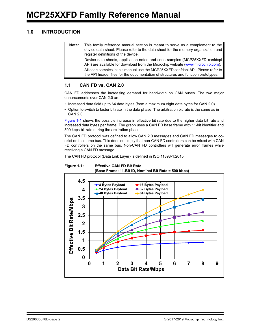
Figure 1-1: Effective CAN FD Bit Rate (Base Frame: 11-Bit ID, Nominal Bit Rate = 500 kbps)
1.2 Features
1.3 Module Block Diagram
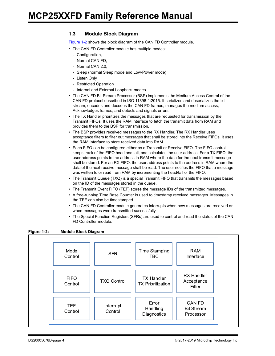
Figure 1-2: Module Block Diagram
1.4 CAN FD Message Frames
1.4.1 ISO vs. Non-ISO CRC
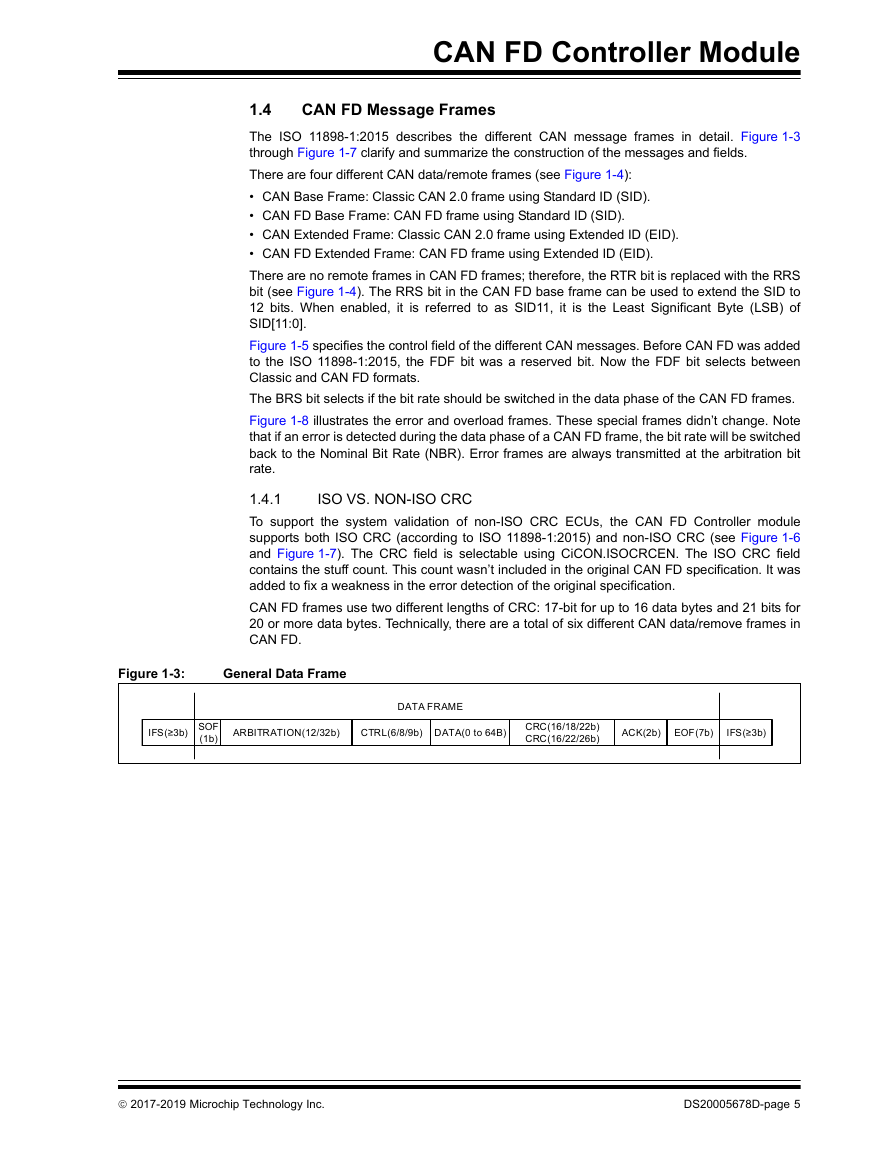
Figure 1-3: General Data Frame
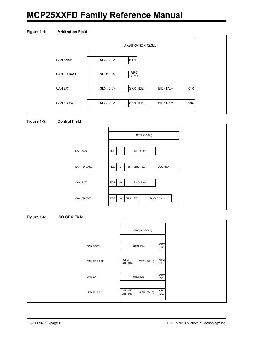
Figure 1-4: Arbitration Field
Figure 1-5: Control Field
Figure 1-6: ISO CRC Field
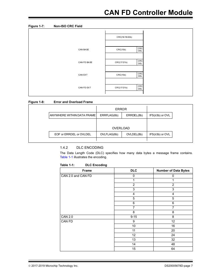
Figure 1-7: Non-ISO CRC Field
Figure 1-8: Error and Overload Frame
1.4.2 DLC Encoding
Table 1-1: DLC Encoding
2.0 Modes of Operation
2.1 Mode Change
2.1.1 Changing Between Normal Modes
2.1.2 Changing Between Debug Modes
2.1.3 Exiting Normal Mode
2.1.4 Entering and Exiting Sleep Mode
2.1.5 Integrating
Figure 2-1: Modes of Operation
2.2 Configuration Mode
2.3 Normal Modes
2.3.1 Normal CAN FD Mode
2.3.2 Normal CAN 2.0 Mode
2.4 Sleep Mode(1,2)
2.4.1 Exiting Sleep mode
2.5 Low-Power Mode (LPM)(1,2,3)
2.5.1 Exiting LPM
2.6 Debug Modes
2.6.1 Listen Only Mode
2.6.2 Restricted Operation Mode
2.6.3 Loopback Mode
3.0 Configuration
3.1 Oscillator Configuration
3.1.1 Crystal/Resonator Selection
Figure 3-1: MCP251XFD Oscillator Block Diagram
3.2 Input/Output Pin Configuration
3.3 CAN Configuration
3.3.1 ISO CRC Enable
3.3.2 Protocol Exception Disable
3.3.3 Wake-up Filter
3.3.4 Restriction of Transmission Attempts
3.3.5 Error State Indicator (ESI) in Gateway Mode
3.3.6 Mode Selection in Case of System Error
3.3.7 Reserving Message Memory for TX Queue and Transmit Event FIFO
3.4 CAN FD Bit Time Configuration
Equation 3-1: Nominal Bit Rate/Time
Equation 3-2: Data Bit Rate/Time
Equation 3-3: Nominal Time Quanta
Equation 3-4: Data Time Quanta
Figure 3-2: Partition of Bit Time
Equation 3-5: Number of NTQ in a NBT
Equation 3-6: Number of DTQ in a DBT
Table 3-1: Nominal Bit Rate Configuration Ranges
Table 3-2: Data Bit Rate Configuration Ranges
3.4.1 Sample Point
Equation 3-7: Nominal Sample Point (%)
Equation 3-8: Data Sample Point (%)
3.4.2 Propagation Delay
Equation 3-9: Maximum Propagation Delay
Figure 3-3: Propagation Delay
3.4.3 Transmitter Delay Compensation (TDC)
Equation 3-10: Secondary Sample Point
Figure 3-4: Measurement of Transceiver Delay (TDCV)
3.4.4 Synchronization
3.4.5 Synchronization Jump Width
3.4.6 Oscillator Tolerance
Equation 3-11: Oscillator Tolerance
Equation 3-12: Condition 1
Equation 3-13: Condition 2
Equation 3-14: Condition 3
Equation 3-15: Condition 4
Equation 3-16: Condition 5
3.4.7 Recommendations for Bit Time Configuration
3.4.8 Bit Time Configuration Example
Table 3-3: Step-by-Step Nominal Bit Rate Configuration
Table 3-4: Step-by-Step Data Bit Rate Configuration
Table 3-5: Bit Time Register Initialization (500k/2M)
3.5 Message Memory Configuration
Figure 3-5: Message Memory Organization
3.5.1 Transmit Event FIFO Configuration
3.5.2 Transmit Queue Configuration
3.5.3 Transmit FIFO Configuration
3.5.4 Receive FIFO Configuration
3.5.5 Calculation of Required Message Memory
Equation 3-17: Size of TEF
Equation 3-18: Size of TXQ
Equation 3-19: Size of FIFOs
Equation 3-20: Total RAM Usage
3.6 Configuration Code Example
Example 3-1: Basic Configuration
Example 3-2: Initialize RAM, Select Normal Mode
4.0 Message Transmission
4.1 Transmit Message Object
4.2 Loading Messages into a Transmit FIFO
Equation 4-1: Address of Next Message Object
4.3 Loading Messages Into the Transmit Queue
TABLE 4-1: Transmit message object (TXQ AND TX FIFO)
4.4 Requesting Transmission of a Message in a Transmit FIFO
4.5 Requesting Transmission of a Message in the Transmit Queue
4.6 CiTXREQ Register
4.7 Transmit Priority
4.7.1 Transmit Priority of Messages Inside a FIFO
4.7.2 Transmit Priority of Messages Inside the TXQ
4.7.3 Transmit Priority Based on ID
4.8 Transmit Bandwidth Sharing
4.9 Retransmission Attempts
4.9.1 Retransmission Attempts Disabled
4.9.2 Three Retransmission Attempts
4.9.3 Unlimited Retransmissions
4.10 Aborting a Transmission
4.11 Remote Transmit Request
4.12 Mismatch of DLC and Payload Size During Transmission
4.13 Transmit State Diagram
Figure 4-1: Transmit State Diagram
4.14 Resetting a Transmit FIFO
4.15 Resetting the Transmit Queue (TXQ)
4.16 Message Transmission Code Example
Example 4-1: Transmit Message from TX FIFO
5.0 Transmit Event FIFO
5.1 Reading a TEF Object
Equation 5-1: Address of Next TEF Object
5.2 Resetting the Transmit Event FIFO (TEF)
TABLE 5-1: Transmit Event FIFO Object
5.3 TEF Code Example
Example 5-1: Reading a Message from the TEF
6.0 Message Filtering
6.1 Filter Configuration
6.2 Filtering a Received Message
Figure 6-1: Message Filtering Flow
6.2.1 Filtering Standard or Extended Frames
6.2.2 Mask Bits
Figure 6-2: Filter Match
6.2.3 Filtering on Data Bytes
6.2.4 12-Bit Standard ID
Table 6-1: Data Byte Filter Configuration
Figure 6-3: CAN Operation with DeviceNet™ Filtering
6.3 Filter Configuration Code Example
Example 6-1: Filter Configuration to Match a Standard Frame Range
7.0 Message Reception
7.1 Receive Message Object
7.1.1 Reading a Receive Message Object
Equation 7-1: Address of next Message Object
TABLE 7-1: Receive message object
7.2 Receive State Diagram
Figure 7-1: Receive State Diagram
7.3 Resetting an RX FIFO
7.4 Mismatch of DLC and Payload Size During Reception
7.5 Message Reception Code Example
Example 7-1: Receiving a Message
8.0 FIFO Behavior
Table 8-1: Example FIFO Configuration
8.1 FIFO Status Flags
8.1.1 TX FIFO Status Flags
8.1.2 RX FIFO Status Flags
8.1.3 TXQ Status Flags
8.1.4 TEF Status Flags
8.2 Transmit FIFO Behavior
Figure 8-1: FIFO 1 – Initial State
Figure 8-2: FIFO 1 – First Message Loaded
Figure 8-3: FIFO 1 – First Message Transmitted
Figure 8-4: FIFO 1 – Three More Messages Loaded
Figure 8-5: FIFO 1 – FIFO Fully Loaded
Figure 8-6: FIFO 1 – FIFO Fully Transmitted
8.3 Receive FIFO Behavior
Figure 8-7: FIFO 2 – Initial State
Figure 8-8: FIFO 2 – First Message Received
Figure 8-9: FIFO 2 – First Message Read
Figure 8-10: FIFO 2 – Half Full
Figure 8-11: FIFO 2 – FIFO Almost Full
Figure 8-12: FIFO 2 – FIFO Full
Figure 8-13: FIFO 2 – FIFO Overflow
Figure 8-14: FIFO 2 – Two More Messages Read
8.4 Transmit Queue Behavior
Figure 8-15: TXQ – Initial State
Figure 8-16: TXQ – First Message Loaded
Figure 8-17: TXQ – First Message Transmitted
Figure 8-18: TXQ – Next Message Loaded
Figure 8-19: TXQ – Next Six Messages Loaded
Figure 8-20: TXQ – Full
8.5 Transmit Event FIFO Behavior
Figure 8-21: TEF – Initial State
Figure 8-22: TEF – First Transmit Message was Stored
Figure 8-23: TEF – First ID Read
Figure 8-24: TEF – Half Full
Figure 8-25: TEF – Almost Full
Figure 8-26: TEF – Full
Figure 8-27: TEF – Overflow
Figure 8-28: TEF – One More ID Read
9.0 Timestamping
Table 9-1: Reference Point
9.1 TBC Configuration Code Example
Example 9-1: Configuration of TBC
10.0 Interrupts
Figure 10-1: Interrupt Multiplexing
10.1 FIFO Individual Interrupts
10.1.1 Transmit Queue (TXQ) Interrupts
10.1.2 Receive FIFO Interrupt – RFIF
10.1.3 Transmit FIFO Interrupt – TFIF
10.1.4 Receive FIFO Overrun Interrupt – RXOVIF
10.1.5 Transmit FIFO Attempt Interrupt – TXATIF
10.1.6 Transmit Event FIFO Interrupt – TEFIF
10.2 MCP25XXFD SPI CRC Interrupts
10.3 MCP25XXFD RAM ECC Interrupts
10.4 FIFO Combined Interrupts
10.5 Main Interrupts
10.5.1 Invalid Message Interrupt – IVMIF
10.5.2 Wake-up Interrupt – WAKIF
10.5.3 CAN Bus Error Interrupt – CERRIF
10.5.4 CAN Mode Change Interrupt – MODIF
10.5.5 CAN Time Base Counter Interrupt – TBCIF
10.5.6 System Error Interrupt – SERRIF
10.5.7 SPI CRC Interrupt – SPICRCIF
10.5.8 ECC Interrupt – ECCIF
10.6 Interrupt Handling
10.6.1 Interrupt Lookup Table
10.6.2 Interrupt Status Registers
10.7 Interrupt Flags
Table 10-1: Interrupt Flags
10.8 Interrupt Configuration and Handling Code Examples
Example 10-1: Configuration of Interrupts
Example 10-2: Using TX Interrupt Pin to Check if TXQ is Ready for Transmission
Example 10-3: Using RX Interrupt Pin to Check if FIFO 2 Contains a New Message
11.0 Error Handling
Figure 11-1: Error States
11.1 Recovery from Bus Off State
12.0 Appendix A: MCP25XXFD CAN FD SPI API
12.1 Introduction
12.2 Abstraction Model
Figure 12-1: Hardware Abstraction Model
12.3 Getting Started with the SPI Communication
12.3.1 SPI Initialization Code Example
Example 12-1: SPI Initialization Function
12.3.2 SPI Data Transfer Code Example
Example 12-2: SPI Data Transfer Function
12.3.3 SPI Read and Write Access Functions
Example 12-3: SPI Access Functions
12.3.4 Verification of the SPI Communication
Example 12-4: Verifying SPI Communication Using RAM Access
Example 12-5: Verifying SPI Communication Using Register Access
13.0 Related Documents
14.0 Revision History
Revision D (May 2019)
Revision C (April 2019)
Revision B (May 2018)
Revision A (September 2017)
Worldwide Sales and Service
CAN FD Controller Module HIGHLIGHTS This section of the manual contains the following major topics: 1.0 Introduction ....................................................................................................................... 2 2.0 Modes of Operation .......................................................................................................... 8 3.0 Configuration................................................................................................................... 13 4.0 Message Transmission ................................................................................................... 26 5.0 Transmit Event FIFO....................................................................................................... 33 6.0 Message Filtering............................................................................................................ 36 7.0 Message Reception ........................................................................................................ 41 FIFO Behavior................................................................................................................. 45 8.0 9.0 Timestamping.................................................................................................................. 58 10.0 Interrupts......................................................................................................................... 59 11.0 Error Handling................................................................................................................. 68 12.0 Appendix A: MCP25XXFD CAN FD SPI API .................................................................. 70 13.0 Related Documents ........................................................................................................ 76 14.0 Revision History .............................................................................................................. 77  2017-2019 Microchip Technology Inc. DS20005678D-page 1
MCP25XXFD Family Reference Manual 1.0 INTRODUCTION Note: This family reference manual section is meant to serve as a complement to the device data sheet. Please refer to the data sheet for the memory organization and register definitions of the device. Device data sheets, application notes and code samples (MCP25XXFD canfdspi API) are available for download from the Microchip website (www.microchip.com). All code samples in this manual use the MCP25XXFD canfdspi API. Please refer to the API header files for the documentation of structures and function prototypes. CAN FD vs. CAN 2.0 1.1 CAN FD addresses the increasing demand for bandwidth on CAN buses. The two major enhancements over CAN 2.0 are: • Increased data field up to 64 data bytes (from a maximum eight data bytes for CAN 2.0). • Option to switch to faster bit rate in the data phase. The arbitration bit rate is the same as in CAN 2.0. Figure 1-1 shows the possible increase in effective bit rate due to the higher data bit rate and increased data bytes per frame. The graph uses a CAN FD base frame with 11-bit identifier and 500 kbps bit rate during the arbitration phase. The CAN FD protocol was defined to allow CAN 2.0 messages and CAN FD messages to co- exist on the same bus. This does not imply that non-CAN FD controllers can be mixed with CAN FD controllers on the same bus. Non-CAN FD controllers will generate error frames while receiving a CAN FD message. The CAN FD protocol (Data Link Layer) is defined in ISO 11898-1:2015. Figure 1-1: Effective CAN FD Bit Rate (Base Frame: 11-Bit ID, Nominal Bit Rate = 500 kbps) 8 Bytes Payload 24 Bytes Payload 48 Bytes Payload 16 Bytes Payload 32 Bytes Payload 64 Bytes Payload 45 4 35 3 25 2 15 1 05 0 s p b M e t a R / t i B e v i t c e f f E 0 1 3 2 Data Bit Rate/Mbps 4 5 6 7 8 9 DS20005678D-page 2  2017-2019 Microchip Technology Inc.
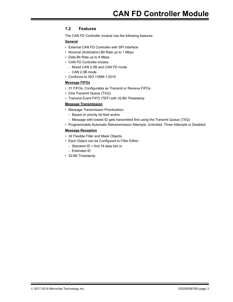
CAN FD Controller Module Features 1.2 The CAN FD Controller module has the following features: General • External CAN FD Controller with SPI Interface • Nominal (Arbitration) Bit Rate up to 1 Mbps • Data Bit Rate up to 8 Mbps • CAN FD Controller modes: - Mixed CAN 2.0B and CAN FD mode - CAN 2.0B mode • Conforms to ISO 11898-1:2015 Message FIFOs • 31 FIFOs, Configurable as Transmit or Receive FIFOs • One Transmit Queue (TXQ) • Transmit Event FIFO (TEF) with 32-Bit Timestamp Message Transmission • Message Transmission Prioritization: - Based on priority bit field and/or - Message with lowest ID gets transmitted first using the Transmit Queue (TXQ) • Programmable Automatic Retransmission Attempts: Unlimited, Three Attempts or Disabled Message Reception • 32 Flexible Filter and Mask Objects • Each Object can be Configured to Filter Either: - Standard ID + first 18 data bits or - Extended ID • 32-Bit Timestamp  2017-2019 Microchip Technology Inc. DS20005678D-page 3
MCP25XXFD Family Reference Manual Module Block Diagram 1.3 Figure 1-2 shows the block diagram of the CAN FD Controller module. • The CAN FD Controller module has multiple modes: - Configuration, - Normal CAN FD, - Normal CAN 2.0, - Sleep (normal Sleep mode and Low-Power mode) - Listen Only - Restricted Operation - Internal and External Loopback modes • The CAN FD Bit Stream Processor (BSP) implements the Medium Access Control of the CAN FD protocol described in ISO 11898-1:2015. It serializes and deserializes the bit stream, encodes and decodes the CAN FD frames, manages the medium access, Acknowledges frames, and detects and signals errors. • The TX Handler prioritizes the messages that are requested for transmission by the Transmit FIFOs. It uses the RAM interface to fetch the transmit data from RAM and provides them to the BSP for transmission. • The BSP provides received messages to the RX Handler. The RX Handler uses acceptance filters to filter out messages that shall be stored into the Receive FIFOs. It uses the RAM Interface to store received data into RAM. • Each FIFO can be configured either as a Transmit or Receive FIFO. The FIFO control keeps track of the FIFO head and tail, and calculates the user address. For a TX FIFO, the user address points to the address in RAM where the data for the next transmit message shall be stored. For an RX FIFO, the user address points to the address in RAM where the data of the next receive message shall be read. The user notifies the FIFO that a message was written to or read from RAM by incrementing the head/tail of the FIFO. • The Transmit Queue (TXQ) is a special Transmit FIFO that transmits the messages based on the ID of the messages stored in the queue. • The Transmit Event FIFO (TEF) stores the message IDs of the transmitted messages. • A free-running Time Base Counter is used to timestamp received messages. Messages in the TEF can also be timestamped. • The CAN FD Controller module generates interrupts when new messages are received or when messages were transmitted successfully. • The Special Function Registers (SFRs) are used to control and read the status of the CAN FD Controller module. Figure 1-2: Module Block Diagram Mode Control FIFO Control TEF Control SFR Time Stamping TBC RAM Interface TXQ Control TX Handler TX Prioritization Interrupt Control Error Handling Diagnostics RX Handler Acceptance Filter CAN FD Bit Stream Processor DS20005678D-page 4  2017-2019 Microchip Technology Inc.
CAN FD Controller Module CAN FD Message Frames 1.4 The ISO 11898-1:2015 describes the different CAN message frames in detail. Figure 1-3 through Figure 1-7 clarify and summarize the construction of the messages and fields. There are four different CAN data/remote frames (see Figure 1-4): • CAN Base Frame: Classic CAN 2.0 frame using Standard ID (SID). • CAN FD Base Frame: CAN FD frame using Standard ID (SID). • CAN Extended Frame: Classic CAN 2.0 frame using Extended ID (EID). • CAN FD Extended Frame: CAN FD frame using Extended ID (EID). There are no remote frames in CAN FD frames; therefore, the RTR bit is replaced with the RRS bit (see Figure 1-4). The RRS bit in the CAN FD base frame can be used to extend the SID to 12 bits. When enabled, it is referred to as SID11, it is the Least Significant Byte (LSB) of SID[11:0]. Figure 1-5 specifies the control field of the different CAN messages. Before CAN FD was added to the ISO 11898-1:2015, the FDF bit was a reserved bit. Now the FDF bit selects between Classic and CAN FD formats. The BRS bit selects if the bit rate should be switched in the data phase of the CAN FD frames. Figure 1-8 illustrates the error and overload frames. These special frames didn’t change. Note that if an error is detected during the data phase of a CAN FD frame, the bit rate will be switched back to the Nominal Bit Rate (NBR). Error frames are always transmitted at the arbitration bit rate. ISO VS. NON-ISO CRC 1.4.1 To support the system validation of non-ISO CRC ECUs, the CAN FD Controller module supports both ISO CRC (according to ISO 11898-1:2015) and non-ISO CRC (see Figure 1-6 and Figure 1-7). The CRC field is selectable using CiCON.ISOCRCEN. The ISO CRC field contains the stuff count. This count wasn’t included in the original CAN FD specification. It was added to fix a weakness in the error detection of the original specification. CAN FD frames use two different lengths of CRC: 17-bit for up to 16 data bytes and 21 bits for 20 or more data bytes. Technically, there are a total of six different CAN data/remove frames in CAN FD. Figure 1-3: General Data Frame IFS(≥3b) SOF (1b) ARBITRATION(12/32b) CTRL(6/8/9b) DATA(0 to 64B) CRC(16/18/22b) CRC(16/22/26b) ACK(2b) EOF(7b) IFS(≥3b) DATA FRAME  2017-2019 Microchip Technology Inc. DS20005678D-page 5
MCP25XXFD Family Reference Manual Figure 1-4: Arbitration Field ARBITRATION(12/32b) CAN BASE SID<10:0> RTR CAN FD BASE SID<10:0> RRS SID11 CAN EXT SID<10:0> SRR IDE EID<17:0> RTR CAN FD EXT SID<10:0> SRR IDE EID<17:0> RRS Figure 1-5: Control Field CTRL(6/8/9b) CAN BASE IDE FDF DLC<3:0> CAN FD BASE IDE FDF res BRS ESI DLC<3:0> CAN EXT FDF r0 DLC<3:0> CAN FD EXT FDF res BRS ESI DLC<3:0> Figure 1-6: ISO CRC Field CRC(16/22/26b) CAN BASE CRC(15b) CAN FD BASE STUFF CNT (4b) CRC(17/21b) CAN EXT CRC(15b) CAN FD EXT STUFF CNT (4b) CRC(17/21b) CRC DEL CRC DEL CRC DEL CRC DEL DS20005678D-page 6  2017-2019 Microchip Technology Inc.
CAN FD Controller Module Figure 1-7: Non-ISO CRC Field CRC(16/18/22b) CAN BASE CRC(15b) CAN FD BASE CRC(17/21b) CAN EXT CRC(15b) CAN FD EXT CRC(17/21b) CRC DEL CRC DEL CRC DEL CRC DEL Figure 1-8: Error and Overload Frame ANYWHERE WITHIN DATA FRAME ERRFLAG(6b) ERRDEL(8b) IFS(≥3b) or OVL ERROR EOF or ERRDEL or OVLDEL OVLFLAG(6b) OVLDEL(8b) IFS(≥3b) or OVL OVERLOAD DLC ENCODING 1.4.2 The Data Length Code (DLC) specifies how many data bytes a message frame contains. Table 1-1 illustrates the encoding. Table 1-1: DLC Encoding Frame CAN 2.0 and CAN FD CAN 2.0 CAN FD DLC Number of Data Bytes 0 1 2 3 4 5 6 7 8 9-15 9 10 11 12 13 14 15 0 1 2 3 4 5 6 7 8 8 12 16 20 24 32 48 64  2017-2019 Microchip Technology Inc. DS20005678D-page 7
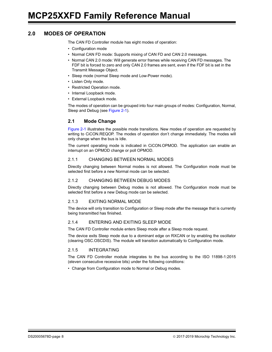
MCP25XXFD Family Reference Manual 2.0 MODES OF OPERATION The CAN FD Controller module has eight modes of operation: • Configuration mode • Normal CAN FD mode: Supports mixing of CAN FD and CAN 2.0 messages. • Normal CAN 2.0 mode: Will generate error frames while receiving CAN FD messages. The FDF bit is forced to zero and only CAN 2.0 frames are sent, even if the FDF bit is set in the Transmit Message Object. • Sleep mode (normal Sleep mode and Low-Power mode). • Listen Only mode. • Restricted Operation mode. • Internal Loopback mode. • External Loopback mode. The modes of operation can be grouped into four main groups of modes: Configuration, Normal, Sleep and Debug (see Figure 2-1). Mode Change 2.1 Figure 2-1 illustrates the possible mode transitions. New modes of operation are requested by writing to CiCON.REQOP. The modes of operation don’t change immediately. The modes will only change when the bus is Idle. The current operating mode is indicated in CiCON.OPMOD. The application can enable an interrupt on an OPMOD change or poll OPMOD. CHANGING BETWEEN NORMAL MODES 2.1.1 Directly changing between Normal modes is not allowed. The Configuration mode must be selected first before a new Normal mode can be selected. CHANGING BETWEEN DEBUG MODES 2.1.2 Directly changing between Debug modes is not allowed. The Configuration mode must be selected first before a new Debug mode can be selected. EXITING NORMAL MODE 2.1.3 The device will only transition to Configuration or Sleep mode after the message that is currently being transmitted has finished. ENTERING AND EXITING SLEEP MODE 2.1.4 The CAN FD Controller module enters Sleep mode after a Sleep mode request. The device exits Sleep mode due to a dominant edge on RXCAN or by enabling the oscillator (clearing OSC.OSCDIS). The module will transition automatically to Configuration mode. INTEGRATING 2.1.5 The CAN FD Controller module integrates to the bus according to the ISO 11898-1:2015 (eleven consecutive recessive bits) under the following conditions: • Change from Configuration mode to Normal or Debug modes. DS20005678D-page 8  2017-2019 Microchip Technology Inc.
分享到:
收藏