ACS712
Fully Integrated, Hall Effect-Based Linear Current Sensor
with 2.1 kVRMS Voltage Isolation and a Low-Resistance Current Conductor
Features and Benefits
▪ Low-noise analog signal path
▪ Device bandwidth is set via the new FILTER pin
▪ 5 μs output rise time in response to step input current
▪ 80 kHz bandwidth
▪ Total output error 1.5% at TA = 25°C
▪ Small footprint, low-profile SOIC8 package
▪ 1.2 mΩ internal conductor resistance
▪ 2.1 kVRMS minimum isolation voltage from pins 1-4 to pins 5-8
▪ 5.0 V, single supply operation
▪ 66 to 185 mV/A output sensitivity
▪ Output voltage proportional to AC or DC currents
▪ Factory-trimmed for accuracy
▪ Extremely stable output offset voltage
▪ Nearly zero magnetic hysteresis
▪ Ratiometric output from supply voltage
TÜV America
Certificate Number:
U8V 06 05 54214 010
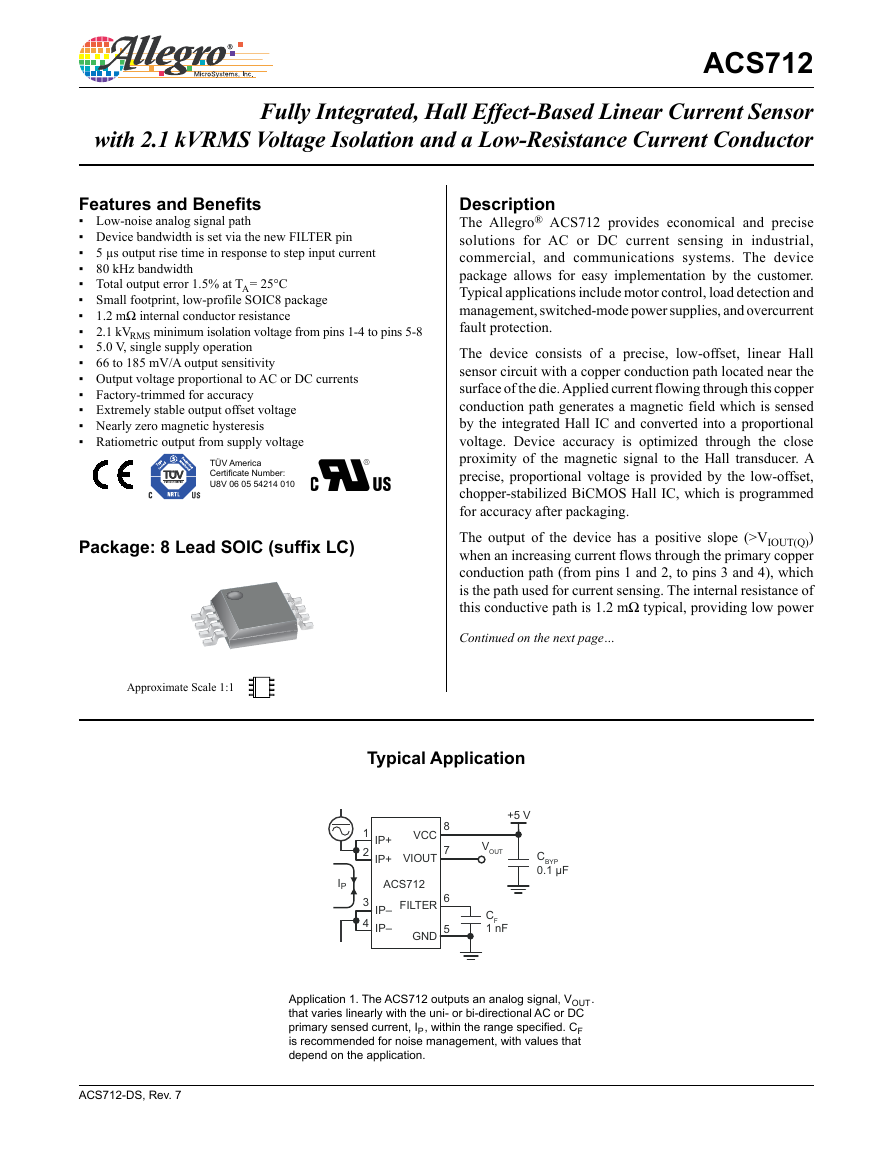
Package: 8 Lead SOIC (suffix LC)
Approximate Scale 1:1
Description
The Allegro® ACS712 provides economical and precise
solutions for AC or DC current sensing in industrial,
commercial, and communications systems. The device
package allows for easy implementation by the customer.
Typical applications include motor control, load detection and
management, switched-mode power supplies, and overcurrent
fault protection.
The device consists of a precise, low-offset, linear Hall
sensor circuit with a copper conduction path located near the
surface of the die. Applied current flowing through this copper
conduction path generates a magnetic field which is sensed
by the integrated Hall IC and converted into a proportional
voltage. Device accuracy is optimized through the close
proximity of the magnetic signal to the Hall transducer. A
precise, proportional voltage is provided by the low-offset,
chopper-stabilized BiCMOS Hall IC, which is programmed
for accuracy after packaging.
The output of the device has a positive slope (>VIOUT(Q))
when an increasing current flows through the primary copper
conduction path (from pins 1 and 2, to pins 3 and 4), which
is the path used for current sensing. The internal resistance of
this conductive path is 1.2 mΩ typical, providing low power
Continued on the next page…
Typical Application
IP
1
2
3
4
IP+
IP+
VCC
VIOUT
ACS712
IP–
IP–
FILTER
GND
8
7
6
5
+5 V
VOUT
CF
1 nF
CBYP
0.1 μF
Application 1. The ACS712 outputs an analog signal, VOUT .
that varies linearly with the uni- or bi-directional AC or DC
primary sensed current, IP , within the range specified. CF
is recommended for noise management, with values that
depend on the application.
ACS712-DS, Rev. 7
�
ACS712
Fully Integrated, Hall Effect-Based Linear Current Sensor with
2.1 kVRMS Voltage Isolation and a Low-Resistance Current Conductor
Description (continued)
loss. The thickness of the copper conductor allows survival of
the device at up to 5× overcurrent conditions. The terminals of
the conductive path are electrically isolated from the sensor leads
(pins 5 through 8). This allows the ACS712 current sensor to be
used in applications requiring electrical isolation without the use
of opto-isolators or other costly isolation techniques.
The ACS712 is provided in a small, surface mount SOIC8 package.
The leadframe is plated with 100% matte tin, which is compatible
with standard lead (Pb) free printed circuit board assembly processes.
Internally, the device is Pb-free, except for flip-chip high-temperature
Pb-based solder balls, currently exempt from RoHS. The device is
fully calibrated prior to shipment from the factory.
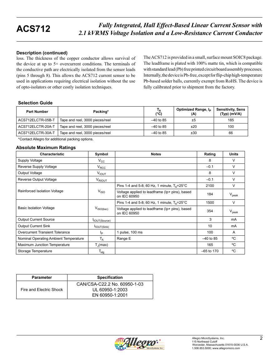
Selection Guide
Part Number
Packing*
Tape and reel, 3000 pieces/reel
Tape and reel, 3000 pieces/reel
Tape and reel, 3000 pieces/reel
ACS712ELCTR-05B-T
ACS712ELCTR-20A-T
ACS712ELCTR-30A-T
*Contact Allegro for additional packing options.
Absolute Maximum Ratings
Characteristic
Supply Voltage
Reverse Supply Voltage
Output Voltage
Reverse Output Voltage
Reinforced Isolation Voltage
Basic Isolation Voltage
Output Current Source
Output Current Sink
Overcurrent Transient Tolerance
Nominal Operating Ambient Temperature
Maximum Junction Temperature
Storage Temperature
Symbol
VCC
VRCC
VIOUT
VRIOUT
VISO
VISO(bsc)
IIOUT(Source)
IIOUT(Sink)
IP
TA
TJ(max)
Tstg
TA
(°C)
–40 to 85
–40 to 85
–40 to 85
Optimized Range, IP
(A)
±5
±20
±30
Sensitivity, Sens
(Typ) (mV/A)
185
100
66
Notes
Rating
Units
Pins 1-4 and 5-8; 60 Hz, 1 minute, TA=25°C
Voltage applied to leadframe (Ip+ pins), based
on IEC 60950
Pins 1-4 and 5-8; 60 Hz, 1 minute, TA=25°C
Voltage applied to leadframe (Ip+ pins), based
on IEC 60950
1 pulse, 100 ms
Range E
8
–0.1
8
–0.1
2100
184
1500
354
3
10
100
–40 to 85
165
–65 to 170
V
V
V
V
V
Vpeak
V
Vpeak
mA
mA
A
ºC
ºC
ºC
Parameter
Specification
Fire and Electric Shock
CAN/CSA-C22.2 No. 60950-1-03
UL 60950-1:2003
EN 60950-1:2001
Allegro MicroSystems, Inc.
115 Northeast Cutoff
Worcester, Massachusetts 01615-0036 U.S.A.
1.508.853.5000; www.allegromicro.com
2
�
ACS712
Fully Integrated, Hall Effect-Based Linear Current Sensor with
2.1 kVRMS Voltage Isolation and a Low-Resistance Current Conductor
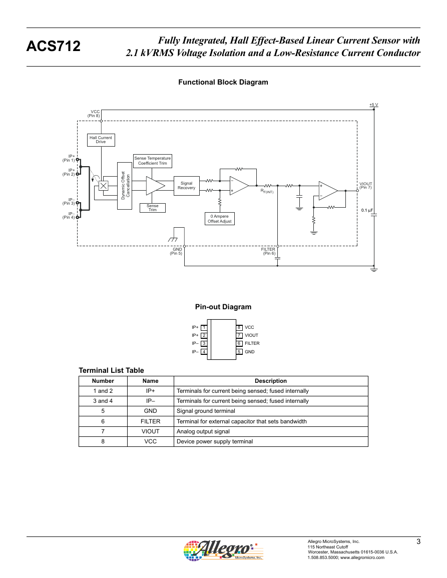
Functional Block Diagram
+5 V
VCC
(Pin 8)
Hall Current
Drive
Sense Temperature
Coefficient Trim
t
n
o
i
t
a
l
l
e
s
f
f
i
O
c
m
a
n
y
D
e
c
n
a
C
Signal
Recovery
RF(INT)
VIOUT
(Pin 7)
Sense
Trim
0 Ampere
Offset Adjust
GND
(Pin 5)
FILTER
(Pin 6)
IP+
(Pin 1)
IP+
(Pin 2)
IP−
(Pin 3)
IP−
(Pin 4)
Pin-out Diagram
IP+
IP+
IP–
IP–
1
2
3
4
8
7
6
5
VCC
VIOUT
FILTER
GND
Terminal List Table
Number
1 and 2
3 and 4
5
6
7
8
Name
IP+
IP–
GND
FILTER
VIOUT
VCC
Description
Terminals for current being sensed; fused internally
Terminals for current being sensed; fused internally
Signal ground terminal
Terminal for external capacitor that sets bandwidth
Analog output signal
Device power supply terminal
Allegro MicroSystems, Inc.
115 Northeast Cutoff
Worcester, Massachusetts 01615-0036 U.S.A.
1.508.853.5000; www.allegromicro.com
3
�
ACS712
Fully Integrated, Hall Effect-Based Linear Current Sensor with
2.1 kVRMS Voltage Isolation and a Low-Resistance Current Conductor
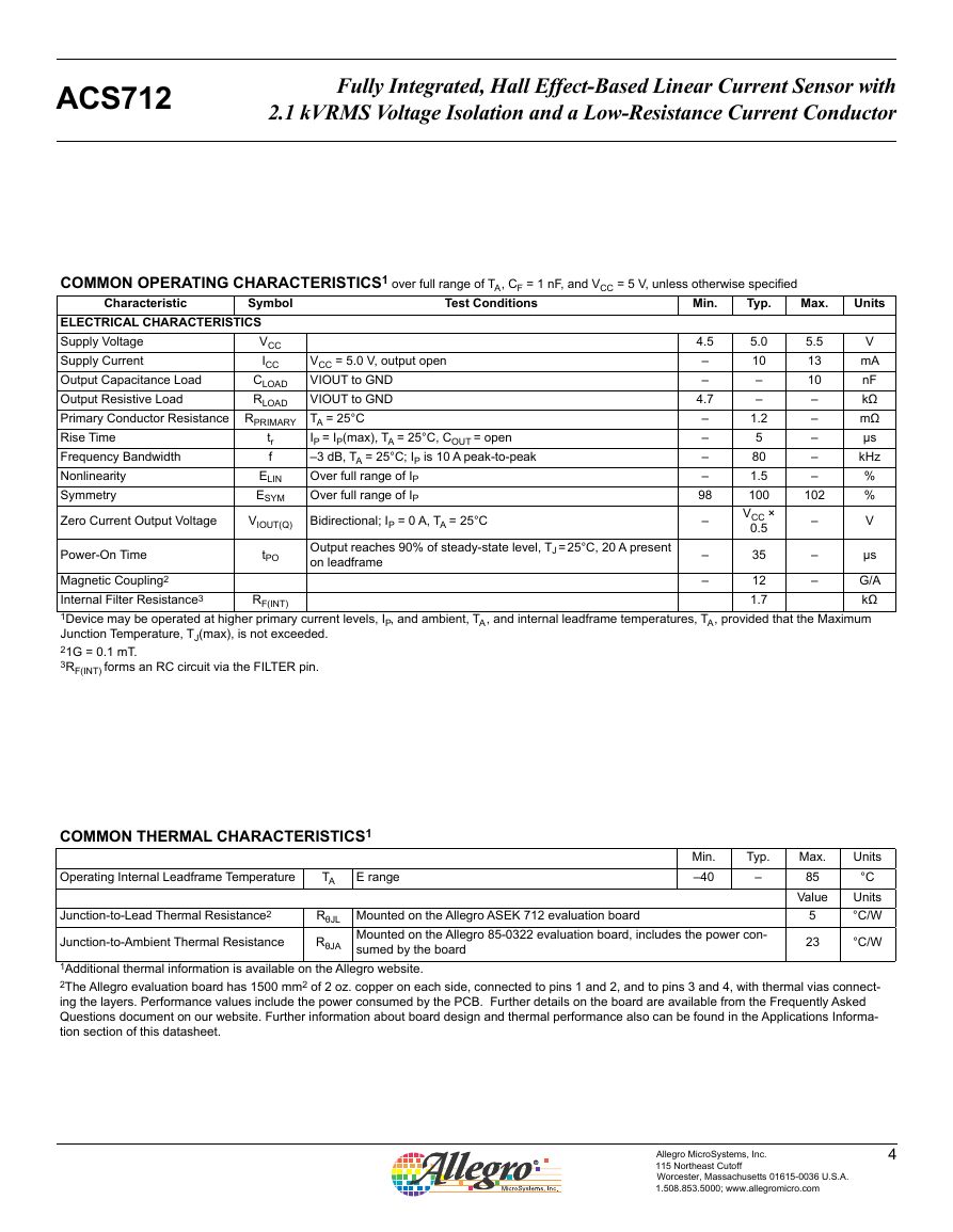
COMMON OPERATING CHARACTERISTICS1 over full range of TA , CF = 1 nF, and VCC = 5 V, unless otherwise specified
Test Conditions
Min.
Typ.
Max.
Units
Characteristic
Symbol
VCC
ICC
CLOAD
RLOAD
ELECTRICAL CHARACTERISTICS
Supply Voltage
Supply Current
Output Capacitance Load
Output Resistive Load
Primary Conductor Resistance RPRIMARY TA = 25°C
Rise Time
Frequency Bandwidth
Nonlinearity
Symmetry
tr
f
ELIN
ESYM
VIOUT(Q)
Zero Current Output Voltage
Power-On Time
tPO
4.5
–
–
4.7
–
–
–
–
98
–
–
5.0
10
–
–
1.2
5
80
1.5
100
VCC ×
0.5
35
5.5
13
10
–
–
–
–
–
102
–
–
V
mA
nF
kΩ
mΩ
μs
kHz
%
%
V
μs
VCC = 5.0 V, output open
VIOUT to GND
VIOUT to GND
IP = IP(max), TA = 25°C, COUT = open
–3 dB, TA = 25°C; IP is 10 A peak-to-peak
Over full range of IP
Over full range of IP
Bidirectional; IP = 0 A, TA = 25°C
Output reaches 90% of steady-state level, TJ = 25°C, 20 A present
on leadframe
Magnetic Coupling2
G/A
Internal Filter Resistance3
kΩ
1Device may be operated at higher primary current levels, IP, and ambient, TA , and internal leadframe temperatures, TA , provided that the Maximum
Junction Temperature, TJ(max), is not exceeded.
21G = 0.1 mT.
3RF(INT) forms an RC circuit via the FILTER pin.
RF(INT)
12
1.7
–
–
COMMON THERMAL CHARACTERISTICS1
Operating Internal Leadframe Temperature
TA
E range
Min.
–40
Typ.
–
Junction-to-Lead Thermal Resistance2
Junction-to-Ambient Thermal Resistance
RθJL Mounted on the Allegro ASEK 712 evaluation board
RθJA
Mounted on the Allegro 85-0322 evaluation board, includes the power con-
sumed by the board
Max.
85
Value
5
23
Units
°C
Units
°C/W
°C/W
1Additional thermal information is available on the Allegro website.
2The Allegro evaluation board has 1500 mm2 of 2 oz. copper on each side, connected to pins 1 and 2, and to pins 3 and 4, with thermal vias connect-
ing the layers. Performance values include the power consumed by the PCB. Further details on the board are available from the Frequently Asked
Questions document on our website. Further information about board design and thermal performance also can be found in the Applications Informa-
tion section of this datasheet.
Allegro MicroSystems, Inc.
115 Northeast Cutoff
Worcester, Massachusetts 01615-0036 U.S.A.
1.508.853.5000; www.allegromicro.com
4
�
ACS712
Fully Integrated, Hall Effect-Based Linear Current Sensor with
2.1 kVRMS Voltage Isolation and a Low-Resistance Current Conductor
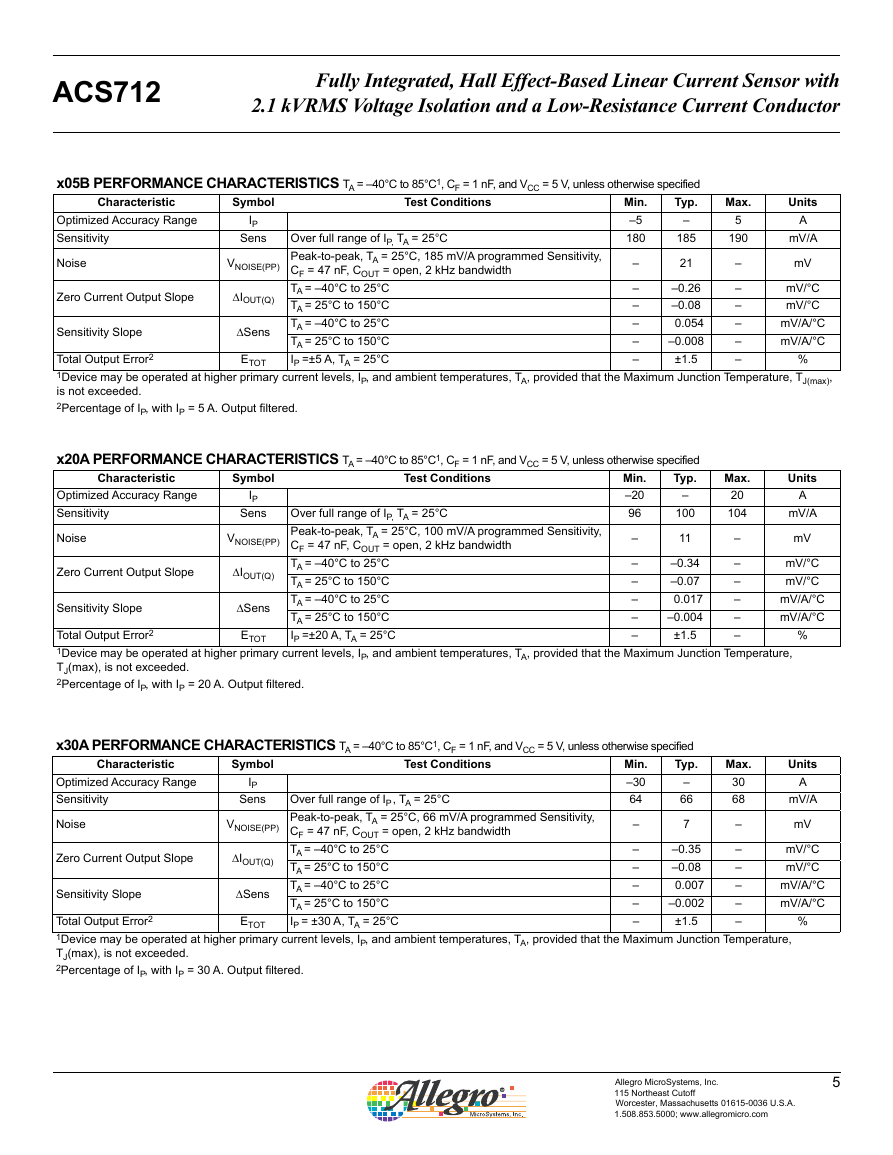
x05B PERFORMANCE CHARACTERISTICS TA = –40°C to 85°C1, CF = 1 nF, and VCC = 5 V, unless otherwise specified
Typ.
Test Conditions
Characteristic
Symbol
Optimized Accuracy Range
Sensitivity
Noise
Zero Current Output Slope
Sensitivity Slope
IP
Sens
VNOISE(PP)
∆IOUT(Q)
∆Sens
Over full range of IP, TA = 25°C
Peak-to-peak, TA = 25°C, 185 mV/A programmed Sensitivity,
CF = 47 nF, COUT = open, 2 kHz bandwidth
TA = –40°C to 25°C
TA = 25°C to 150°C
TA = –40°C to 25°C
TA = 25°C to 150°C
IP =±5 A, TA = 25°C
Total Output Error2
1Device may be operated at higher primary current levels, IP, and ambient temperatures, TA, provided that the Maximum Junction Temperature, TJ(max),
is not exceeded.
2Percentage of IP, with IP = 5 A. Output filtered.
ETOT
%
x20A PERFORMANCE CHARACTERISTICS TA = –40°C to 85°C1, CF = 1 nF, and VCC = 5 V, unless otherwise specified
Typ.
Test Conditions
Characteristic
Symbol
Optimized Accuracy Range
Sensitivity
Noise
Zero Current Output Slope
Sensitivity Slope
IP
Sens
VNOISE(PP)
∆IOUT(Q)
∆Sens
Over full range of IP, TA = 25°C
Peak-to-peak, TA = 25°C, 100 mV/A programmed Sensitivity,
CF = 47 nF, COUT = open, 2 kHz bandwidth
TA = –40°C to 25°C
TA = 25°C to 150°C
TA = –40°C to 25°C
TA = 25°C to 150°C
IP =±20 A, TA = 25°C
Total Output Error2
1Device may be operated at higher primary current levels, IP, and ambient temperatures, TA, provided that the Maximum Junction Temperature,
TJ(max), is not exceeded.
2Percentage of IP, with IP = 20 A. Output filtered.
ETOT
%
x30A PERFORMANCE CHARACTERISTICS TA = –40°C to 85°C1, CF = 1 nF, and VCC = 5 V, unless otherwise specified
Typ.
Test Conditions
Characteristic
Symbol
Optimized Accuracy Range
Sensitivity
Noise
Zero Current Output Slope
Sensitivity Slope
IP
Sens
VNOISE(PP)
∆IOUT(Q)
∆Sens
Over full range of IP , TA = 25°C
Peak-to-peak, TA = 25°C, 66 mV/A programmed Sensitivity,
CF = 47 nF, COUT = open, 2 kHz bandwidth
TA = –40°C to 25°C
TA = 25°C to 150°C
TA = –40°C to 25°C
TA = 25°C to 150°C
IP = ±30 A , TA = 25°C
Total Output Error2
1Device may be operated at higher primary current levels, IP, and ambient temperatures, TA, provided that the Maximum Junction Temperature,
TJ(max), is not exceeded.
2Percentage of IP, with IP = 30 A. Output filtered.
ETOT
Min.
–5
180
Min.
–20
96
–
–
–
–
–
–
–
–
–
–
–
–
–
–
–
–
–
–
Min.
–30
64
–
185
21
–0.26
–0.08
0.054
–0.008
±1.5
–
100
11
–0.34
–0.07
0.017
–0.004
±1.5
–
66
7
–0.35
–0.08
0.007
–0.002
±1.5
Max.
5
190
–
Max.
20
104
–
–
–
–
–
–
–
–
–
–
–
–
–
–
–
–
Max.
30
68
–
Units
A
mV/A
mV
mV/°C
mV/°C
mV/A/°C
mV/A/°C
Units
A
mV/A
mV
mV/°C
mV/°C
mV/A/°C
mV/A/°C
Units
A
mV/A
mV
mV/°C
mV/°C
mV/A/°C
mV/A/°C
%
Allegro MicroSystems, Inc.
115 Northeast Cutoff
Worcester, Massachusetts 01615-0036 U.S.A.
1.508.853.5000; www.allegromicro.com
5
�
ACS712
Fully Integrated, Hall Effect-Based Linear Current Sensor with
2.1 kVRMS Voltage Isolation and a Low-Resistance Current Conductor
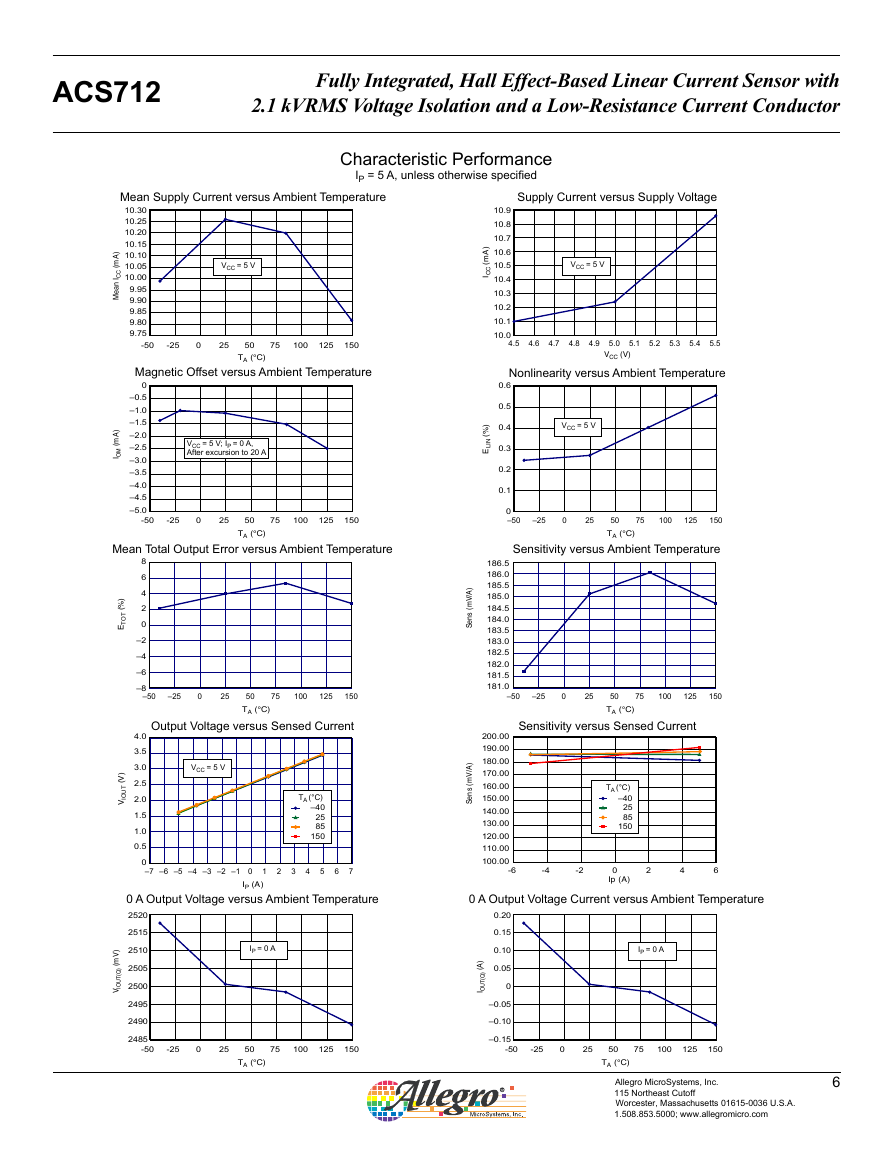
Characteristic Performance
IP = 5 A, unless otherwise specified
Mean Supply Current versus Ambient Temperature
10.30
10.25
10.20
10.15
10.10
10.05
10.00
9.95
9.90
9.85
9.80
9.75
VCC = 5 V
)
A
m
(
C
C
I
n
a
e
M
-50
-25
0
25
50
75
100
125
150
TA (°C)
Magnetic Offset versus Ambient Temperature
0
–0.5
–1.0
–1.5
–2.0
–2.5
–3.0
–3.5
–4.0
–4.5
–5.0
VCC = 5 V; IP = 0 A,
After excursion to 20 A
)
A
m
(
M
O
I
-50
-25
0
25
50
75
100
125
150
TA (°C)
Mean Total Output Error versus Ambient Temperature
8
6
4
2
0
–2
–4
–6
–8
–50
–25
0
25
75
100
125
150
50
TA (°C)
Output Voltage versus Sensed Current
VCC = 5 V
)
%
(
T
O
T
E
)
V
(
T
U
O
V
I
4.0
3.5
3.0
2.5
2.0
1.5
1.0
0.5
TA (°C)
–40
25
85
150
2
3
4
5
6
7
0
–7 –6 –5 –4 –3 –2 –1 0
1
IP (A)
0 A Output Voltage versus Ambient Temperature
2520
)
V
m
(
)
Q
(
T
U
O
V
I
2515
2510
2505
2500
2495
2490
2485
-50
IP = 0 A
-25
0
25
50
75
100
125
150
TA (°C)
Supply Current versus Supply Voltage
)
A
m
(
C
C
I
10.9
10.8
10.7
10.6
10.5
10.4
10.3
10.2
10.1
10.0
4.5
VCC = 5 V
4.6
4.7
4.8
4.9
5.1
5.0
VCC (V)
5.2
5.3
5.4
5.5
Nonlinearity versus Ambient Temperature
0.6
VCC = 5 V
)
%
(
I
N
L
E
0.5
0.4
0.3
0.2
0.1
0
–50
–25
0
25
75
100
125
150
50
TA (°C)
Sensitivity versus Ambient Temperature
186.5
186.0
185.5
185.0
184.5
184.0
183.5
183.0
182.5
182.0
181.5
181.0
–50
–25
0
25
50
TA (°C)
75
100
125
150
)
/
A
V
m
(
s
n
e
S
)
/
A
V
m
(
s
n
e
S
200.00
190.00
180.00
170.00
160.00
150.00
140.00
130.00
120.00
110.00
100.00
-6
Sensitivity versus Sensed Current
TA (°C)
–40
25
85
150
-4
-2
0
Ip (A)
2
4
6
0 A Output Voltage Current versus Ambient Temperature
)
A
(
)
Q
(
T
U
O
I
0.20
0.15
0.10
0.05
0
–0.05
–0.10
–0.15
-50
IP = 0 A
-25
0
25
50
75
100
125
150
TA (°C)
Allegro MicroSystems, Inc.
115 Northeast Cutoff
Worcester, Massachusetts 01615-0036 U.S.A.
1.508.853.5000; www.allegromicro.com
6
�
ACS712
Fully Integrated, Hall Effect-Based Linear Current Sensor with
2.1 kVRMS Voltage Isolation and a Low-Resistance Current Conductor
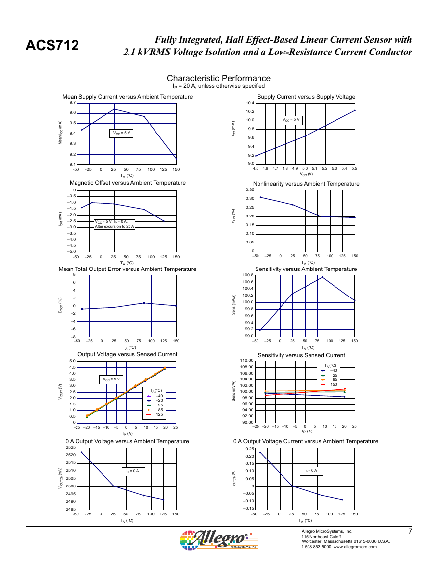
Characteristic Performance
IP = 20 A, unless otherwise specified
Mean Supply Current versus Ambient Temperature
9.7
)
A
m
(
C
C
I
n
a
e
M
)
A
m
(
M
O
I
9.6
9.5
9.4
9.3
9.2
9.1
-50
VCC = 5 V
-25
0
25
50
75
100
125
150
TA (°C)
Magnetic Offset versus Ambient Temperature
0
–0.5
–1.0
–1.5
–2.0
–2.5
–3.0
–3.5
–4.0
–4.5
–5.0
VCC = 5 V; IP = 0 A,
After excursion to 20 A
-50
-25
0
25
50
75
100
125
150
)
A
m
(
C
C
I
)
%
(
I
N
L
E
TA (°C)
Supply Current versus Supply Voltage
VCC = 5 V
10.4
10.2
10.0
9.8
9.6
9.4
9.2
9.0
4.5
4.6
4.7
4.8
4.9
5.1
5.0
VCC (V)
5.2
5.3
5.4
5.5
Nonlinearity versus Ambient Temperature
0.35
0.30
0.25
0.20
0.15
0.10
0.05
0
–50
–25
0
25
Mean Total Output Error versus Ambient Temperature
Sensitivity versus Ambient Temperature
75
100
125
150
50
TA (°C)
-25
0
25
50
75
100
125
150
-50
-25
0
25
50
75
100
125
150
TA (°C)
TA (°C)
Allegro MicroSystems, Inc.
115 Northeast Cutoff
Worcester, Massachusetts 01615-0036 U.S.A.
1.508.853.5000; www.allegromicro.com
7
)
/
A
V
m
(
s
n
e
S
)
/
A
V
m
(
s
n
e
S
100.8
100.6
100.4
100.2
100.0
99.8
99.6
99.4
99.2
99.0
110.00
108.00
106.00
104.00
102.00
100.00
98.00
96.00
94.00
92.00
90.00
8
6
4
2
0
–2
–4
–6
–8
–50
–25
0
25
75
100
125
150
50
TA (°C)
Output Voltage versus Sensed Current
VCC = 5 V
5.0
4.5
4.0
3.5
3.0
2.5
2.0
1.5
1.0
0.5
0
–25 –20 –15 –10
TA (°C)
–40
–20
25
85
125
5
10
15
20
25
–5
0
IP (A)
0 A Output Voltage versus Ambient Temperature
2525
IP = 0 A
)
%
(
T
O
T
E
)
V
(
T
U
O
V
I
)
V
m
(
)
Q
(
T
U
O
V
I
2520
2515
2510
2505
2500
2495
2490
2485
-50
–50
–25
0
25
50
TA (°C)
75
100
125
150
Sensitivity versus Sensed Current
TA (°C)
–40
25
85
150
–25 –20 –15 –10
–5
5
0
Ip (A)
10
15
20
25
0 A Output Voltage Current versus Ambient Temperature
)
A
(
)
Q
(
T
U
O
I
0.25
0.20
0.15
0.10
0.05
0
–0.05
–0.10
–0.15
IP = 0 A
�
ACS712
Fully Integrated, Hall Effect-Based Linear Current Sensor with
2.1 kVRMS Voltage Isolation and a Low-Resistance Current Conductor
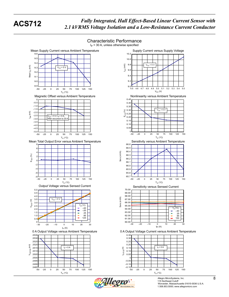
Characteristic Performance
IP = 30 A, unless otherwise specified
Mean Supply Current versus Ambient Temperature
9.6
)
A
m
(
C
C
I
n
a
e
M
)
A
m
(
M
O
I
VCC = 5 V
9.5
9.4
9.3
9.2
9.1
9.0
8.9
-50
-25
0
25
50
75
100
125
150
TA (°C)
Magnetic Offset versus Ambient Temperature
0
–0.5
–1.0
–1.5
–2.0
–2.5
–3.0
–3.5
–4.0
–4.5
–5.0
VCC = 5 V; IP = 0 A,
After excursion to 20 A
-50
-25
0
25
50
75
100
125
150
Mean Total Output Error versus Ambient Temperature
TA (°C)
Supply Current versus Supply Voltage
VCC = 5 V
)
A
m
(
C
C
I
10.2
10.0
9.8
9.6
9.4
9.2
9.0
4.5
4.6
4.7
4.8
4.9
5.1
5.0
VCC (V)
5.2
5.3
5.4
5.5
Nonlinearity versus Ambient Temperature
)
%
(
I
N
L
E
0.45
0.40
0.35
0.30
0.25
0.20
0.15
0.10
0.05
0
–50
VCC = 5 V
–25
0
25
50
TA (°C)
75
100
125
150
Sensitivity versus Ambient Temperature
TA (°C)
–40
25
85
150
–20
–10
0
Ip (A)
10
20
30
0 A Output Voltage Current versus Ambient Temperature
)
A
(
)
Q
(
T
U
O
I
0.35
0.30
0.25
0.20
0.15
0.10
0.05
0
–0.05
–0.10
–0.15
-50
IP = 0 A
-25
0
25
50
75
100
125
150
TA (°C)
Allegro MicroSystems, Inc.
115 Northeast Cutoff
Worcester, Massachusetts 01615-0036 U.S.A.
1.508.853.5000; www.allegromicro.com
8
75
100
125
150
50
TA (°C)
Output Voltage versus Sensed Current
–50
–25
0
25
50
TA (°C)
75
100
125
150
Sensitivity versus Sensed Current
)
/
A
V
m
(
s
n
e
S
)
/
A
V
m
(
s
n
e
S
66.6
66.5
66.4
66.3
66.2
66.1
66.0
65.9
65.8
65.7
70.00
69.00
68.00
67.00
66.00
65.00
64.00
63.00
62.00
61.00
60.00
–30
)
%
(
T
O
T
E
)
V
(
T
U
O
V
I
8
6
4
2
0
–2
–4
–6
–8
–50
–25
0
25
5.0
4.5
4.0
3.5
3.0
2.5
2.0
1.5
1.0
0.5
0
–30
VCC = 5 V
–20
–10
TA (°C)
–40
–20
25
85
125
10
20
30
0
IP (A)
)
V
m
(
)
Q
(
T
U
O
V
I
0 A Output Voltage versus Ambient Temperature
2535
2530
2525
2520
2515
2510
2505
2500
2495
2490
2485
IP = 0 A
-50
-25
0
25
50
75
100
125
150
TA (°C)
�


 2023年江西萍乡中考道德与法治真题及答案.doc
 2012年重庆南川中考生物真题及答案.doc
 2013年江西师范大学地理学综合及文艺理论基础考研真题.doc
 2020年四川甘孜小升初语文真题及答案I卷.doc
 2020年注册岩土工程师专业基础考试真题及答案.doc
 2023-2024学年福建省厦门市九年级上学期数学月考试题及答案.doc
 2021-2022学年辽宁省沈阳市大东区九年级上学期语文期末试题及答案.doc
 2022-2023学年北京东城区初三第一学期物理期末试卷及答案.doc
 2018上半年江西教师资格初中地理学科知识与教学能力真题及答案.doc
 2012年河北国家公务员申论考试真题及答案-省级.doc
 2020-2021学年江苏省扬州市江都区邵樊片九年级上学期数学第一次质量检测试题及答案.doc
 2022下半年黑龙江教师资格证中学综合素质真题及答案.doc