logo资料库

pg066-jesd204.pdf

第1页 / 共131页
第2页 / 共131页
第3页 / 共131页
第4页 / 共131页
第5页 / 共131页
第6页 / 共131页
第7页 / 共131页
第8页 / 共131页
资料共131页,剩余部分请下载后查看
JESD204 v7.2
Table of Contents
IP Facts
Ch. 1: Overview
Transmitter
Receiver
Core Level Architecture
Applications
Unsupported Features
Licensing and Ordering Information
License Checkers
License Type
License Options
Simulation Only
Full System Hardware Evaluation
Full
Obtaining Your License Key
Simulation License
Full System Hardware Evaluation License
Obtaining a Full License
Installing Your License File
Ch. 2: Product Specification
Standards
Performance
Resource Utilization
Port Descriptions
Clock and Reset Ports – TX Core
Clock and Reset Ports – RX Core
JESD204 PHY and Transceiver Interface Ports – TX Core
JESD204 PHY and Transceiver Interface Ports – RX Core
Transmit Data Interface – TX Core
Receive Data Interface – RX Core
Management Interface (AXI4-Lite)
Transceiver Debug Interface
Register Space
Ch. 3: Designing with the Core
General Design Guidelines
Use the Example Design as a Starting Point
Know the Degree of Difficulty
Keep It Registered
Recognize Timing Critical Signals
Use Supported Design Flows
Make Only Allowed Modifications
Recommended Design Experience
Core Overview and Getting Started
Serial Line Rate and Clocking
Core Clock
Reference Clock
AXI4-Lite Interface Clock
Selecting the Operating Line Rate and Reference Clock
Core Delivery – Shared Logic Example Design
Transceiver Sharing
Subclass Mode
Subclass 0
Subclass 1
Subclass 2
Programming the Core
Clocking
Supporting Subclass 1 and 2 Deterministic Latency
Number of lanes per link
Basic Generic Clocking Schemes
7 Series Devices
UltraScale Devices
7 Series Devices
UltraScale and UltraScale+ Devices
Supported Clock Frequency Ranges
Detailed Clocking
Clocking for Subclass 0 Mode
Resets
System Reset
Software Reset
Watchdog Timer Reset
AXI4-Stream Reset
Interfacing to the AXI4-Stream Data Interface
Transport Layer
TI ADS42JB69 ADC 2 Converter, 4 Lane Mode
ADI AD9250 ADC 2 Converter, 2 Lane Mode
IDT ADC1443D ADC 2 Converter, 2 Lane Mode
AXI4-Lite Management Interface
Subclass 1 Operation
SYSREF Timing
SYSREF Handling
SYSREF Sampling Clock Edge
SYSREF Always
SYSREF on Initial Link Bring-Up
SYSREF on Link Resynchronization
SYSREF Delay
Subclass 2 Operation
JESD204B Receiver
Lane Skew
Elastic Buffer Implementation
Receive Latency
RX End to End Latency
ADC Timing
Core Timing
Calculating End to End Latency
Achieving Repeatable Latency
Procedure - Achieving Repeatable Latency
Minimum Deterministic Latency Support
Error Signaling Using the SYNC~ Interface
Link Re-initialization
JESD204B Transmitter
Transmit Latency
TX End to End Latency
Core Timing
DAC Timing
Calculating End to End Latency
Step 1 – Determine how many LMFC periods are required (N)
Step 2 – Calculate the end to end latency using N
Example
Transmitter Phase Adjustment for Subclass 2
Link Test Modes
Continuous D21.5 Characters
Modified RPAT
JSPAT
Transceiver PRBS test patterns
Link Re-initialization
Sharing Transceivers between Transmit and Receive
Sharing Transceivers in IP Integrator
Sharing a QPLL
Sharing Transceivers in RTL Designs
Powering down unused GT channels
Ch. 4: Design Flow Steps
Customizing and Generating the Core
Configuration Tab
Link Configuration Tab
Shared Logic Tab
JESD204 PHY Configuration Tab
User Parameters
Output Generation
Constraining the Core
Required Constraints
Device, Package, and Speed Grade Selections
Clock Frequencies
SYSREF Constraints
Clock Domains
Clock Management
Clock Placement
Banking
Transceiver Placement
I/O Standard and Placement
Simulation
Synthesis and Implementation
Ch. 5: Example Design
Common Design Elements
Transport Layer Mapping
sysref Generation
TX Block Layout
TX Transport Layer Mapping
RX Block Layout
RX Transport Layer Mapping
Ch. 6: Test Bench
Appx. A: Verification, Compliance, and Interoperability
Simulation
Hardware Testing
Appx. B: Hardware Demonstration Design
Appx. C: Migrating and Upgrading
Migrating to the Vivado Design Suite
Upgrading in the Vivado Design Suite
Device Migration
Upgrading from v7.0 to v7.1
Upgrading from JESD204 v6.2 to v7.0
Upgrading from JESD204 v6.1 to v6.2
Upgrading from JESD204 v6.0 to v6.1
Upgrading from JESD204 v5.2 to v6.0
Transmitter with Shared Logic in Example Design
Transmitter with Shared Logic in Example Design Converted to Include Shared Logic in Core
Receiver with Shared Logic in Example Design
Receiver with Shared Logic in Example Design Converted to Include Shared Logic in Core
Transmitter with Shared Logic in Core
Receiver with Shared Logic in Core
Appx. D: Debugging
Finding Help on Xilinx.com
Documentation
Answer Records
Technical Support
Debug Tools
Vivado Design Suite Debug Feature
Reference Boards
Simulation Debug
Hardware Debug
General Checks
Issues Obtaining Lane Synchronization
Issues Losing Synchronization Soon After Gaining Synchronization
Interface Debug
AXI4-Lite Interfaces
Appx. E: Additional Resources and Legal Notices
Xilinx Resources
References
Revision History
Please Read: Important Legal Notices
JESD204 v7.2 LogiCORE IP Product Guide Vivado Design Suite PG066 October 4, 2017
Table of Contents IP Facts Chapter 1: Overview Transmitter. . . . . . . . . . . . . . . . . . . . . . . . . . . . . . . . . . . . . . . . . . . . . . . . . . . . . . . . . . . . . . . . . . . . . . . 5 Receiver . . . . . . . . . . . . . . . . . . . . . . . . . . . . . . . . . . . . . . . . . . . . . . . . . . . . . . . . . . . . . . . . . . . . . . . . . 6 Core Level Architecture . . . . . . . . . . . . . . . . . . . . . . . . . . . . . . . . . . . . . . . . . . . . . . . . . . . . . . . . . . . . . 7 Applications . . . . . . . . . . . . . . . . . . . . . . . . . . . . . . . . . . . . . . . . . . . . . . . . . . . . . . . . . . . . . . . . . . . . . . 8 Unsupported Features. . . . . . . . . . . . . . . . . . . . . . . . . . . . . . . . . . . . . . . . . . . . . . . . . . . . . . . . . . . . . . 8 Licensing and Ordering Information. . . . . . . . . . . . . . . . . . . . . . . . . . . . . . . . . . . . . . . . . . . . . . . . . . . 9 Chapter 2: Product Specification Standards . . . . . . . . . . . . . . . . . . . . . . . . . . . . . . . . . . . . . . . . . . . . . . . . . . . . . . . . . . . . . . . . . . . . . . . 12 Performance. . . . . . . . . . . . . . . . . . . . . . . . . . . . . . . . . . . . . . . . . . . . . . . . . . . . . . . . . . . . . . . . . . . . . 12 Resource Utilization. . . . . . . . . . . . . . . . . . . . . . . . . . . . . . . . . . . . . . . . . . . . . . . . . . . . . . . . . . . . . . . 12 Port Descriptions . . . . . . . . . . . . . . . . . . . . . . . . . . . . . . . . . . . . . . . . . . . . . . . . . . . . . . . . . . . . . . . . . 13 Register Space . . . . . . . . . . . . . . . . . . . . . . . . . . . . . . . . . . . . . . . . . . . . . . . . . . . . . . . . . . . . . . . . . . . 27 Chapter 3: Designing with the Core General Design Guidelines . . . . . . . . . . . . . . . . . . . . . . . . . . . . . . . . . . . . . . . . . . . . . . . . . . . . . . . . . 41 Core Overview and Getting Started . . . . . . . . . . . . . . . . . . . . . . . . . . . . . . . . . . . . . . . . . . . . . . . . . . 43 Clocking. . . . . . . . . . . . . . . . . . . . . . . . . . . . . . . . . . . . . . . . . . . . . . . . . . . . . . . . . . . . . . . . . . . . . . . . . 46 Resets . . . . . . . . . . . . . . . . . . . . . . . . . . . . . . . . . . . . . . . . . . . . . . . . . . . . . . . . . . . . . . . . . . . . . . . . . . 55 Interfacing to the AXI4-Stream Data Interface . . . . . . . . . . . . . . . . . . . . . . . . . . . . . . . . . . . . . . . . . 56 AXI4-Lite Management Interface . . . . . . . . . . . . . . . . . . . . . . . . . . . . . . . . . . . . . . . . . . . . . . . . . . . . 58 Subclass 1 Operation . . . . . . . . . . . . . . . . . . . . . . . . . . . . . . . . . . . . . . . . . . . . . . . . . . . . . . . . . . . . . . 59 Subclass 2 Operation . . . . . . . . . . . . . . . . . . . . . . . . . . . . . . . . . . . . . . . . . . . . . . . . . . . . . . . . . . . . . . 64 JESD204B Receiver. . . . . . . . . . . . . . . . . . . . . . . . . . . . . . . . . . . . . . . . . . . . . . . . . . . . . . . . . . . . . . . . 64 JESD204B Transmitter . . . . . . . . . . . . . . . . . . . . . . . . . . . . . . . . . . . . . . . . . . . . . . . . . . . . . . . . . . . . . 74 Link Test Modes . . . . . . . . . . . . . . . . . . . . . . . . . . . . . . . . . . . . . . . . . . . . . . . . . . . . . . . . . . . . . . . . . . 78 Sharing Transceivers between Transmit and Receive . . . . . . . . . . . . . . . . . . . . . . . . . . . . . . . . . . . . 80 Chapter 4: Design Flow Steps Customizing and Generating the Core . . . . . . . . . . . . . . . . . . . . . . . . . . . . . . . . . . . . . . . . . . . . . . . . 85 Constraining the Core . . . . . . . . . . . . . . . . . . . . . . . . . . . . . . . . . . . . . . . . . . . . . . . . . . . . . . . . . . . . . 93 JESD204 v7.2 PG066 October 4, 2017 www.xilinx.com 2 Send Feedback
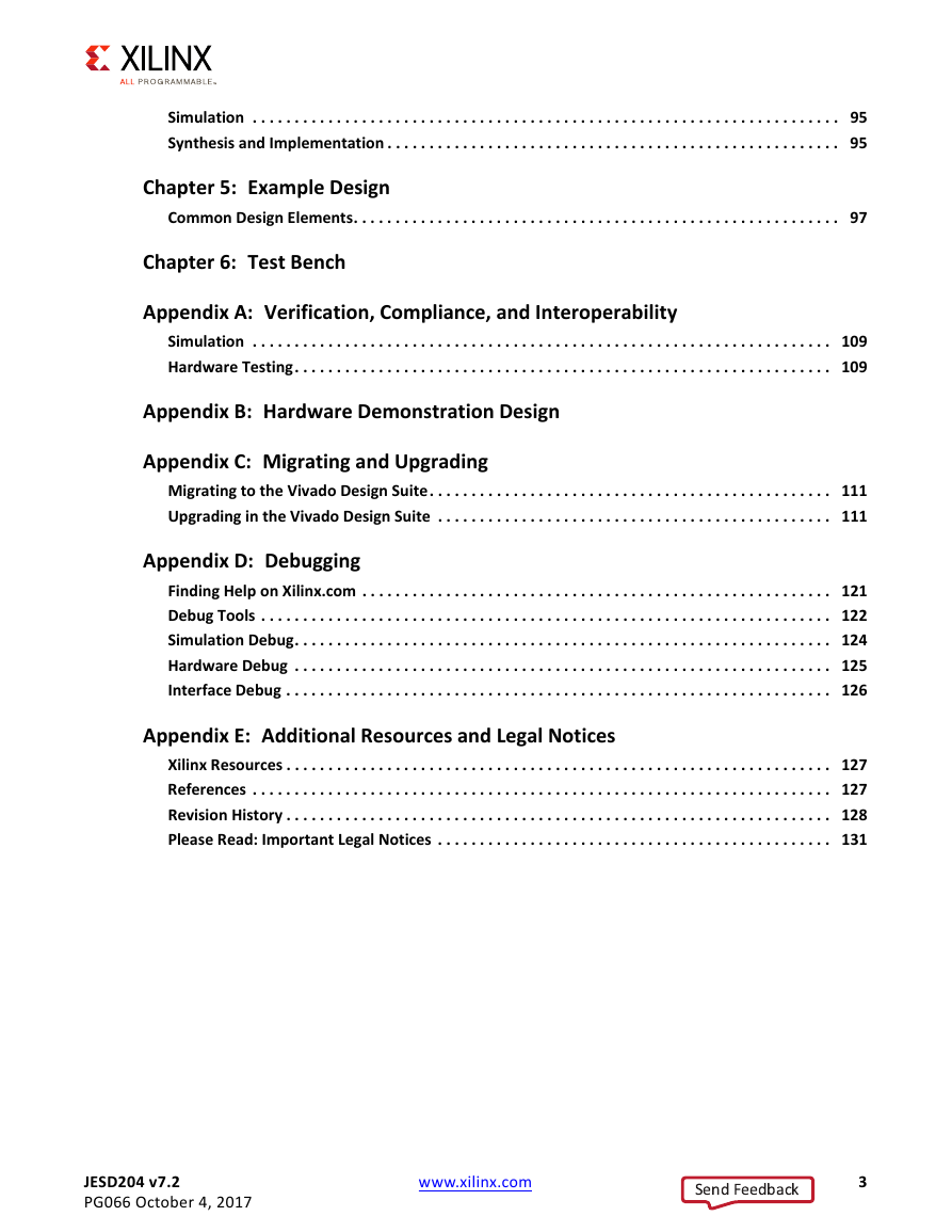
Simulation . . . . . . . . . . . . . . . . . . . . . . . . . . . . . . . . . . . . . . . . . . . . . . . . . . . . . . . . . . . . . . . . . . . . . . 95 Synthesis and Implementation . . . . . . . . . . . . . . . . . . . . . . . . . . . . . . . . . . . . . . . . . . . . . . . . . . . . . . 95 Chapter 5: Example Design Common Design Elements. . . . . . . . . . . . . . . . . . . . . . . . . . . . . . . . . . . . . . . . . . . . . . . . . . . . . . . . . . 97 Chapter 6: Test Bench Appendix A: Verification, Compliance, and Interoperability Simulation . . . . . . . . . . . . . . . . . . . . . . . . . . . . . . . . . . . . . . . . . . . . . . . . . . . . . . . . . . . . . . . . . . . . . 109 Hardware Testing. . . . . . . . . . . . . . . . . . . . . . . . . . . . . . . . . . . . . . . . . . . . . . . . . . . . . . . . . . . . . . . . 109 Appendix B: Hardware Demonstration Design Appendix C: Migrating and Upgrading Migrating to the Vivado Design Suite. . . . . . . . . . . . . . . . . . . . . . . . . . . . . . . . . . . . . . . . . . . . . . . . 111 Upgrading in the Vivado Design Suite . . . . . . . . . . . . . . . . . . . . . . . . . . . . . . . . . . . . . . . . . . . . . . . 111 Appendix D: Debugging Finding Help on Xilinx.com . . . . . . . . . . . . . . . . . . . . . . . . . . . . . . . . . . . . . . . . . . . . . . . . . . . . . . . . 121 Debug Tools . . . . . . . . . . . . . . . . . . . . . . . . . . . . . . . . . . . . . . . . . . . . . . . . . . . . . . . . . . . . . . . . . . . . 122 Simulation Debug. . . . . . . . . . . . . . . . . . . . . . . . . . . . . . . . . . . . . . . . . . . . . . . . . . . . . . . . . . . . . . . . 124 Hardware Debug . . . . . . . . . . . . . . . . . . . . . . . . . . . . . . . . . . . . . . . . . . . . . . . . . . . . . . . . . . . . . . . . 125 Interface Debug . . . . . . . . . . . . . . . . . . . . . . . . . . . . . . . . . . . . . . . . . . . . . . . . . . . . . . . . . . . . . . . . . 126 Appendix E: Additional Resources and Legal Notices Xilinx Resources . . . . . . . . . . . . . . . . . . . . . . . . . . . . . . . . . . . . . . . . . . . . . . . . . . . . . . . . . . . . . . . . . 127 References . . . . . . . . . . . . . . . . . . . . . . . . . . . . . . . . . . . . . . . . . . . . . . . . . . . . . . . . . . . . . . . . . . . . . 127 Revision History . . . . . . . . . . . . . . . . . . . . . . . . . . . . . . . . . . . . . . . . . . . . . . . . . . . . . . . . . . . . . . . . . 128 Please Read: Important Legal Notices . . . . . . . . . . . . . . . . . . . . . . . . . . . . . . . . . . . . . . . . . . . . . . . 131 JESD204 v7.2 PG066 October 4, 2017 www.xilinx.com 3 Send Feedback
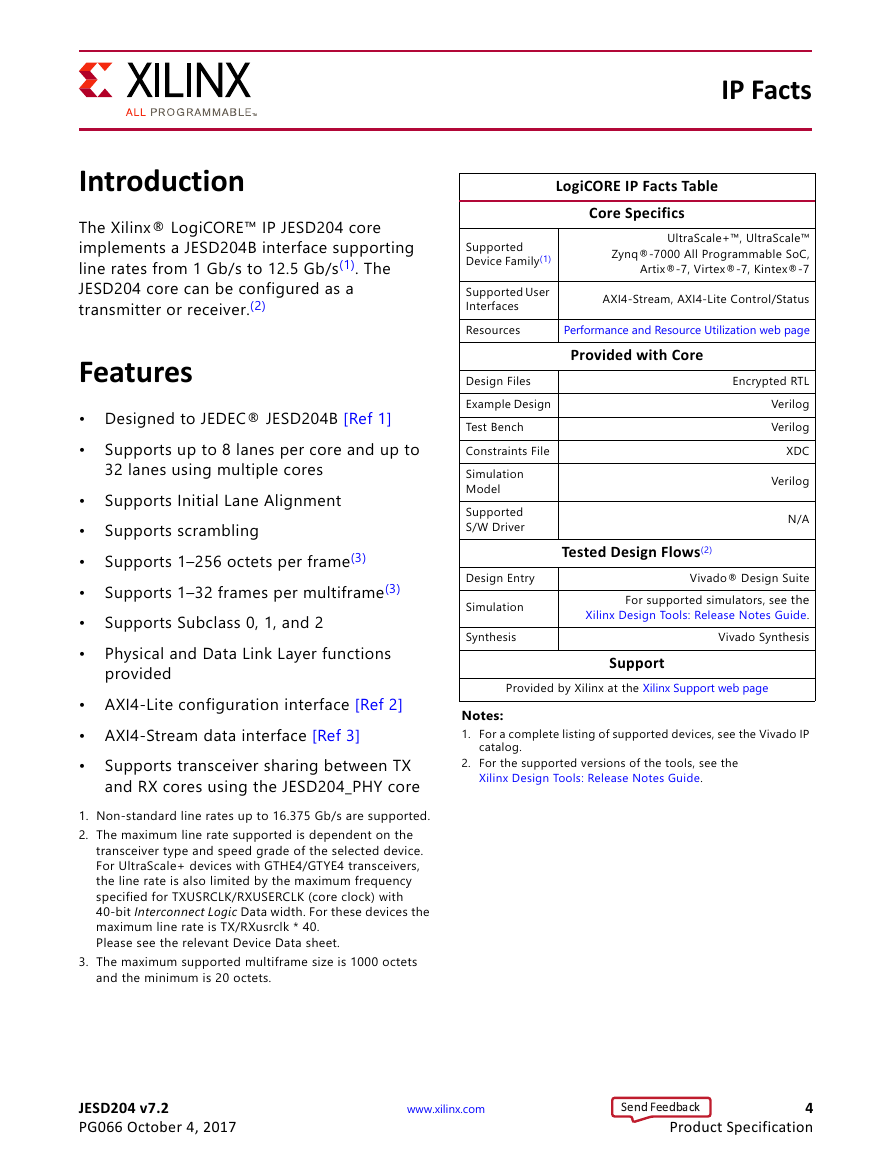
IP Facts LogiCORE IP Facts Table Core Specifics UltraScale+™, UltraScale™ Zynq®-7000 All Programmable SoC, Artix®-7, Virtex®-7, Kintex®-7 AXI4-Stream, AXI4-Lite Control/Status Performance and Resource Utilization web page Provided with Core Encrypted RTL Verilog Verilog XDC Verilog N/A Supported Device Family(1) Supported User Interfaces Resources Design Files Example Design Test Bench Constraints File Simulation Model Supported S/W Driver Tested Design Flows(2) Design Entry Simulation Synthesis Vivado® Design Suite For supported simulators, see the Xilinx Design Tools: Release Notes Guide. Vivado Synthesis Support Provided by Xilinx at the Xilinx Support web page Notes: 1. For a complete listing of supported devices, see the Vivado IP catalog. 2. For the supported versions of the tools, see the Xilinx Design Tools: Release Notes Guide. Introduction The Xilinx® LogiCORE™ IP JESD204 core implements a JESD204B interface supporting line rates from 1 Gb/s to 12.5 Gb/s(1). The JESD204 core can be configured as a transmitter or receiver.(2) Features • Designed to JEDEC® JESD204B [Ref 1] • Supports up to 8 lanes per core and up to 32 lanes using multiple cores Supports Initial Lane Alignment Supports scrambling Supports 1–256 octets per frame(3) Supports 1–32 frames per multiframe(3) Supports Subclass 0, 1, and 2 Physical and Data Link Layer functions provided • • • • • • • AXI4-Lite configuration interface [Ref 2] • AXI4-Stream data interface [Ref 3] • Supports transceiver sharing between TX and RX cores using the JESD204_PHY core 1. Non-standard line rates up to 16.375 Gb/s are supported. 2. The maximum line rate supported is dependent on the transceiver type and speed grade of the selected device. For UltraScale+ devices with GTHE4/GTYE4 transceivers, the line rate is also limited by the maximum frequency specified for TXUSRCLK/RXUSERCLK (core clock) with 40-bit Interconnect Logic Data width. For these devices the maximum line rate is TX/RXusrclk * 40. Please see the relevant Device Data sheet. 3. The maximum supported multiframe size is 1000 octets and the minimum is 20 octets. JESD204 v7.2 PG066 October 4, 2017 www.xilinx.com 4 Product Specification Send Feedback
Chapter 1 Overview The LogiCORE™ IP JESD204 core implements a JESD204B interface supporting line rates between 1 and 12.5 Gb/s(1) on 1 to 8 lanes using GTX, GTH, GTP or GTY (UltraScale and UltraScale+ only) transceivers. See the device data sheets for maximum line rates supported by each device and family. The JESD204 core can be configured as transmit or receive and multiple cores can be used to realize links requiring greater than 8 lanes. The JESD204 core is a fully-verified solution design delivered by using the Xilinx® Vivado® Design Suite. In addition, an example design is provided in Verilog. Transmitter Figure 1-1 shows an overview block diagram for the transmitter of the JESD204 core. X-Ref Target - Figure 1-1 JESD204 Transmitter Core TX Lane(s) AXI4-Stream Scrambler Alignment Character Generator Text Alignment Sequence Lane Text Sync/SYSREF TX Counters AXI4-Lite Control AXI4-Lite/IPIF Registers RPAT Generator JSPAT Generator Y H P _ 4 0 2 D S E J JESD204 Serial Data Figure 1‐1: Transmitter Core Overview 1. Non-standard line rates up to 16.375 Gb/s are supported. JESD204 v7.2 PG066 October 4, 2017 www.xilinx.com 5 Send Feedback
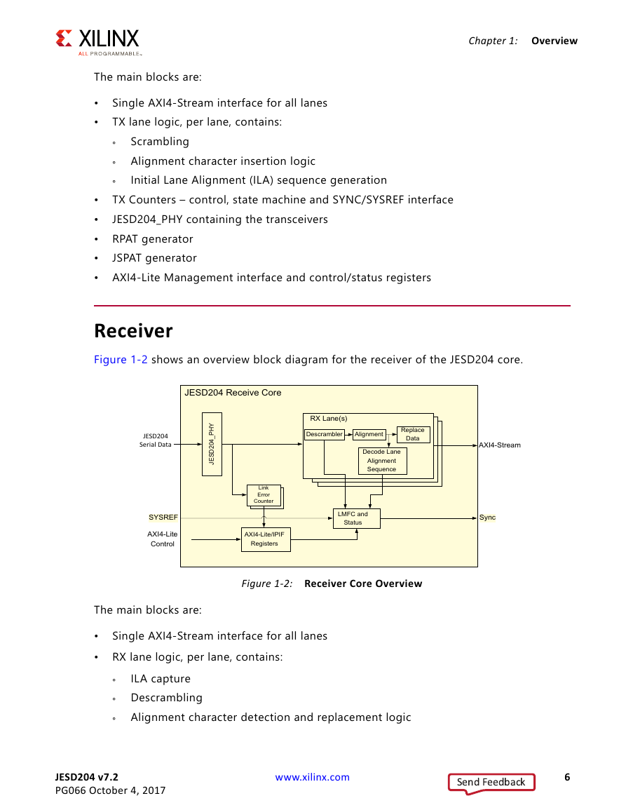
Chapter 1: Overview The main blocks are: • • Scrambling Alignment character insertion logic Initial Lane Alignment (ILA) sequence generation Single AXI4-Stream interface for all lanes TX lane logic, per lane, contains: ° ° ° TX Counters – control, state machine and SYNC/SYSREF interface JESD204_PHY containing the transceivers RPAT generator JSPAT generator • • • • • AXI4-Lite Management interface and control/status registers Receiver Figure 1-2 shows an overview block diagram for the receiver of the JESD204 core. X-Ref Target - Figure 1-2 JESD204 Serial Data Y H P _ 4 0 2 D S E J Figure 1‐2: Receiver Core Overview The main blocks are: • • Single AXI4-Stream interface for all lanes RX lane logic, per lane, contains: ILA capture ° ° Descrambling ° Alignment character detection and replacement logic JESD204 v7.2 PG066 October 4, 2017 www.xilinx.com 6 Send Feedback
Chapter 1: Overview Local Multiframe Clock (LMFC) state machine and SYNC/SYSREF interface JESD204_PHY containing the transceivers Error counters for each lane • • • • AXI4-Lite Management interface and control/status registers Core Level Architecture The JESD204 core is delivered by the Vivado Design Suite with supporting wrapper files. Either a JESD204B transmitter core or a JESD204B receiver core can be selected for generation using the Vivado IDE. Core-level Verilog wrappers are provided to instantiate the JESD204 IP, the clock/reset logic, Management block, the JESD204_PHY transceiver, the JSPAT and RPAT pattern generator blocks, and the Error Counting blocks depending on whether the core is a transmitter or a receiver. The core support layer, delivered with the example design, is intended for instantiation in simple unidirectional designs. The Management block provides core Control and Status registers with a standard AXI4-Lite interface. The RPAT and JSPAT blocks are optional test pattern generators which can be included in a TX core. Link Error counter blocks are included in a receiver core to support data link layer test modes and link status monitoring. A Verilog example design is provided which instantiates the core-level wrapper, together with example interface modules. This is a device-level design and can be used to run the core through the Xilinx tool flow, but is not intended to be used directly in customer designs. The transmit and receive logic is completely independent; a core can be generated as a transmitter or a receiver. The core can be generated with the JESD204 PHY, instantiated either: • Inside the core for basic simplex applications or Inside the example design for applications that require sharing the transceivers with other JESD204 cores (e.g., TX and RX sharing transceivers) or access to the extended features available using JESD204 PHY AXI-lite register interface (see Shared Logic Tab). • JESD204 v7.2 PG066 October 4, 2017 www.xilinx.com 7 Send Feedback
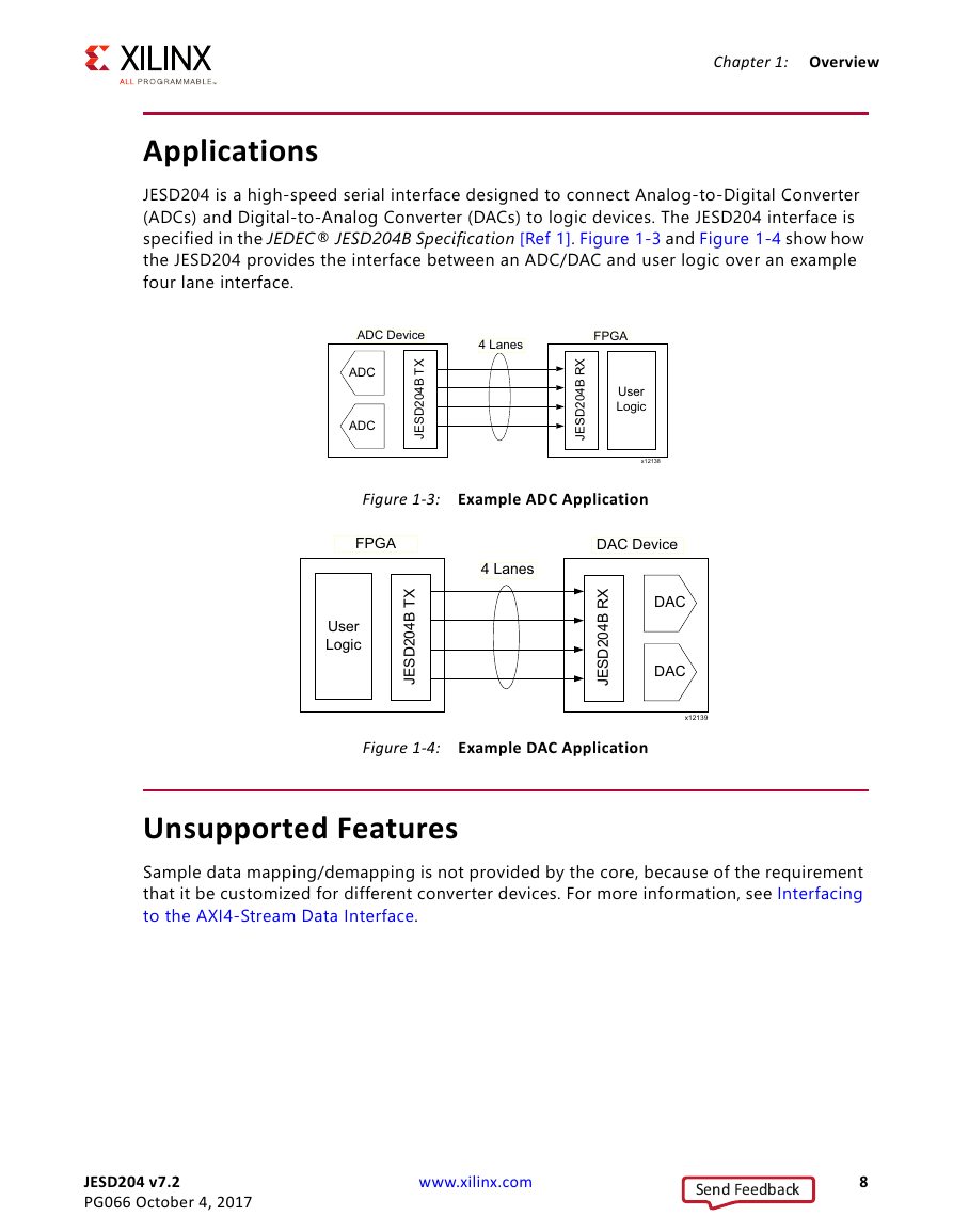
Chapter 1: Overview Applications JESD204 is a high-speed serial interface designed to connect Analog-to-Digital Converter (ADCs) and Digital-to-Analog Converter (DACs) to logic devices. The JESD204 interface is specified in the JEDEC® JESD204B Specification [Ref 1]. Figure 1-3 and Figure 1-4 show how the JESD204 provides the interface between an ADC/DAC and user logic over an example four lane interface. X-Ref Target - Figure 1-3 ADC Device 4 Lanes FPGA ADC ADC X T B 4 0 2 D S E J X R B 4 0 2 D S E J User Logic x12138 Figure 1‐3: Example ADC Application X-Ref Target - Figure 1-4 FPGA DAC Device 4 Lanes User Logic X T B 4 0 2 D S E J X R B 4 0 2 D S E J DAC DAC x12139 Figure 1‐4: Example DAC Application Unsupported Features Sample data mapping/demapping is not provided by the core, because of the requirement that it be customized for different converter devices. For more information, see Interfacing to the AXI4-Stream Data Interface. JESD204 v7.2 PG066 October 4, 2017 www.xilinx.com 8 Send Feedback
分享到:
收藏