logo资料库

KEAZ128数据手册.pdf

第1页 / 共705页
第2页 / 共705页
第3页 / 共705页
第4页 / 共705页
第5页 / 共705页
第6页 / 共705页
第7页 / 共705页
第8页 / 共705页
资料共705页,剩余部分请下载后查看
Chapter 1​: About This Document
Overview
Purpose
Audience
Conventions
Numbering systems
Typographic notation
Special terms
Chapter 2​: Introduction
Overview
Module functional categories
ARM Cortex-M0+ core modules
System modules
Memories and memory interfaces
Clocks
Security and integrity modules
Analog modules
Timer modules
Communication interfaces
Human-machine interfaces
Orderable part numbers
Chapter 3​: Chip Configuration
Introduction
Module to Module Interconnects
Interconnection overview
Analog reference options
ACMP output capture
UART0_TX modulation
UART0/1/2_RX capture
UART0_RX filter
RTC capture
FTM2 software synchronization
ADC hardware trigger
Core Modules
ARM Cortex-M0+ core configuration
ARM Cortex M0+ core
Buses, interconnects, and interfaces
System Tick Timer
Core privilege levels
Caches
Nested Vectored Interrupt Controller (NVIC) configuration
Interrupt priority levels
Non-maskable interrupt
Interrupt channel assignments
Determining the field and register location for configuring a particular interrupt
Asynchronous wakeup interrupt controller (AWIC) configuration
Wakeup sources
System Modules
SIM configuration
PMC configuration
MCM configuration
Crossbar-light switch configuration
Crossbar-Light switch master assignments
Crossbar switch slave assignments
Peripheral bridge configuration
Number of peripheral bridges
Memory maps
System Security
CRC configuration
Watchdog configuration
WDOG clocks
WDOG operation
Clock Modules
ICS configuration
Clock gating
OSC configuration
Memories and Memory Interfaces
Flash memory configuration
Flash memory sizes
Flash memory map
Alternate Non-Volatile IRC User Trim Description
Flash security
Erase all flash contents
Flash memory controller configuration
SRAM configuration
SRAM sizes
SRAM ranges
SRAM bit operation
Analog
12-bit analog-to-digital converter (ADC) configuration
ADC instantiation information
ADC0 connections/channel assignment
ADC analog supply and reference connections
Temperature sensor and bandgap
Alternate clock
ACMP configuration
ACMP overview
ACMP interconnections
ACMP in Stop mode
Timers
FlexTimer configuration
FTM overview
FTM clock options
FTM interconnections
FTM interrupts
PIT configuration
PIT overview
PIT interconnections
RTC configuration
RTC overview
RTC interconnections
PWT configuration
PWT overview
PWT interconnections
Communication interfaces
SPI configuration
SPI overview
I2C configuration
I2C overview
I2C0 4-wire interface feature
UART configuration
UART overview
UART interconnection
MSCAN configuration
MSCAN overview
MSCAN clock source
MSCAN wake-up interrupt and glitch filter
Human-machine interfaces (HMI)
GPIO configuration
GPIO overview
KBI configuration
KBI overview
KBI assignments
IRQ configuration
IRQ assignment
Chapter 4​: Memory Map
Introduction
System memory map
Aliased bit-band region
Bit Manipulation Engine
System ROM memory map
ROM
ROM_ENTRYn
ROM_TABLEMARK
ROM_SYSACCESS
ROM_PERIPHIDn
ROM_COMPIDn
Peripheral bridge (AIPS-Lite) memory map
Read-after-write sequence and required serialization of memory operations
Peripheral Bridge (AIPS-Lite) Memory Map
Private Peripheral Bus (PPB) memory map
Chapter 5​: Clock Distribution
Introduction
Programming model
High-level device clocking diagram
Clock definitions
Device clock summary
Clock distribution
Internal clocking sources
External clock sources
Clock gating
Module clocks
FTM and PWT clocking
Chapter 6​: Reset and Boot
Introduction
Reset
Power-on reset (POR)
System reset sources
External pin reset (RESET)
Reset pin filter
Low-voltage detect (LVD)
Watchdog timer
ICS loss-of-clock (LOC)
Stop mode acknowledge error (SACKERR)
Software reset (SW)
Lockup reset (LOCKUP)
MDM-AP system reset request
MCU resets
Boot
Boot sources
Boot sequence
Chapter 7​: Power Management
Introduction
Power modes
Entering and exiting power modes
Module operation in low-power modes
Chapter 8​: Security
Introduction
Flash security
Security interactions with other modules
Security interactions with debug
Chapter 9​: Debug
Introduction
Debug port pin descriptions
SWD status and control registers
MDM-AP status register
MDM-AP Control register
Debug resets
Debug in low-power modes
Debug and security
Chapter 10​: Signal Multiplexing and Signal Descriptions
Introduction
Pinout
Signal multiplexing and pin assignments
Device pin assignment
Module signal description tables
Core modules
System modules
Clock modules
Analog
Timer modules
Communication Interfaces
Human-machine interfaces (HMI)
Chapter 11​: Port Control (PORT)
Introduction
Port data and data direction
Internal pullup enable
Input glitch filter setting
High current drive
Pin behavior in Stop mode
Port data registers
PORT
PORT_IOFLT0
PORT_IOFLT1
PORT_PUE0
PORT_PUE1
PORT_PUE2
PORT_HDRVE
Chapter 12​: System Integration Module (SIM)
Introduction
Features
Memory map and register definition
SIM
SIM_SRSID
SIM_SOPT0
SIM_SOPT1
SIM_PINSEL0
SIM_PINSEL1
SIM_SCGC
SIM_UUIDL
SIM_UUIDML
SIM_UUIDMH
SIM_CLKDIV
Functional description
Chapter 13​: Power Management Controller (PMC)
Introduction
Low voltage detect (LVD) system
Power-on reset (POR) operation
LVD reset operation
LVD enabled in Stop mode
Low-voltage warning (LVW)
Bandgap reference
Memory map and register descriptions
PMC
PMC_SPMSC1
PMC_SPMSC2
Chapter 14​: Miscellaneous Control Module (MCM)
Introduction
Features
Memory map/register descriptions
MCM
MCM_PLASC
MCM_PLAMC
MCM_PLACR
Chapter 15​: Peripheral Bridge (AIPS-Lite)
Introduction
Features
General operation
Functional description
Access support
Chapter 16​: Watchdog Timer (WDOG)
Introduction
Features
Block diagram
Memory map and register definition
WDOG
WDOG_CS1
WDOG_CS2
WDOG_CNTH
WDOG_CNTL
WDOG_TOVALH
WDOG_TOVALL
WDOG_WINH
WDOG_WINL
Functional description
Watchdog refresh mechanism
Window mode
Refreshing the Watchdog
Example code: Refreshing the Watchdog
Configuring the Watchdog
Reconfiguring the Watchdog
Unlocking the Watchdog
Example code: Reconfiguring the Watchdog
Clock source
Using interrupts to delay resets
Backup reset
Functionality in debug and low-power modes
Fast testing of the watchdog
Testing each byte of the counter
Entering user mode
Chapter 17​: Bit Manipulation Engine (BME)
Introduction
Overview
Features
Modes of operation
Memory map and register definition
Functional description
BME decorated stores
Decorated store logical AND (AND)
Decorated store logical OR (OR)
Decorated store logical XOR (XOR)
Decorated store bit field insert (BFI)
BME decorated loads
Decorated load: load-and-clear 1 bit (LAC1)
Decorated Load: Load-and-Set 1 Bit (LAS1)
Decorated load unsigned bit field extract (UBFX)
Additional details on decorated addresses and GPIO accesses
Application information
Chapter 18​: Flash Memory Module (FTMRE)
Introduction
Feature
Flash memory features
Other flash module features
Functional description
Modes of operation
Wait mode
Stop mode
Flash memory map
Flash initialization after system reset
Flash command operations
Writing the FCLKDIV register
Command write sequence
Flash interrupts
Description of flash interrupt operation
Protection
Security
Unsecuring the MCU using backdoor key access
Unsecuring the MCU using SWD
Mode and security effects on flash command availability
Flash commands
Flash commands
Flash command summary
Erase Verify All Blocks command
Erase Verify Block command
Erase Verify Flash Section command
Read once command
Program Flash command
Program Once command
Erase All Blocks command
Debugger mass erase request
Erase flash block command
Erase flash sector command
Unsecure flash command
Verify backdoor access key command
Set user margin level command
Set factory margin level command
Configure NVM command
Memory map and register definition
FTMRE
FTMRE_FCCOBIX
FTMRE_FSEC
FTMRE_FCLKDIV
FTMRE_FSTAT
FTMRE_FCNFG
FTMRE_FCCOBLO
FTMRE_FCCOBHI
FTMRE_FPROT
FTMRE_FOPT
Chapter 19​: Flash Memory Controller (FMC)
Introduction
Overview
Features
Modes of operation
External signal description
Memory map and register descriptions
Functional description
Chapter 20​: Internal Clock Source (ICS)
Introduction
Features
Block diagram
Modes of operation
FLL engaged internal (FEI)
FLL engaged external (FEE)
FLL bypassed internal (FBI)
FLL bypassed internal low power (FBILP)
FLL bypassed external (FBE)
FLL bypassed external low power (FBELP)
Stop (STOP)
External signal description
Register definition
ICS
ICS_C1
ICS_C2
ICS_C3
ICS_C4
ICS_S
Functional description
Operational modes
FLL engaged internal (FEI)
FLL engaged external (FEE)
FLL bypassed internal (FBI)
FLL bypassed internal low power (FBILP)
FLL bypassed external (FBE)
FLL bypassed external low power (FBELP)
Stop
Mode switching
Bus frequency divider
Low-power field usage
Internal reference clock
Fixed frequency clock
FLL lock and clock monitor
FLL clock lock
External reference clock monitor
Initialization/application information
Initializing FEI mode
Initializing FBI mode
Initializing FEE mode
Initializing FBE mode
Chapter 21​: Oscillator (OSC)
Introduction
Overview
Features and modes
Block diagram
Signal description
External crystal / resonator connections
External clock connections
Memory map and register descriptions
OSC
OSC_CR
Functional description
OSC module states
Off
Oscillator startup
Oscillator stable
External clock mode
OSC module modes
Low-frequency, high-gain mode
Low-frequency, low-power mode
High-frequency, high-gain mode
High-frequency, low-power mode
Counter
Reference clock pin requirements
Chapter 22​: Cyclic Redundancy Check (CRC)
Introduction
Features
Block diagram
Modes of operation
Run mode
Low-power modes (Wait or Stop)
Memory map and register descriptions
CRC
CRC_DATA
CRC_GPOLY
CRC_CTRL
Functional description
CRC initialization/reinitialization
CRC calculations
16-bit CRC
32-bit CRC
Transpose feature
Types of transpose
CRC result complement
Chapter 23​: Interrupt (IRQ)
Introduction
Features
Pin configuration options
Edge and level sensitivity
Interrupt pin request register
IRQ
IRQ_SC
Chapter 24​: Analog-to-digital converter (ADC)
Introduction
Features
Block Diagram
External Signal Description
Analog Power (VDDA)
Analog Ground (VSSA)
Voltage Reference High (VREFH)
Voltage Reference Low (VREFL)
Analog Channel Inputs (ADx)
ADC Control Registers
ADC
ADC_SC1
ADC_SC2
ADC_SC3
ADC_SC4
ADC_R
ADC_CV
ADC_APCTL1
ADC_SC5
Functional description
Clock select and divide control
Input select and pin control
Hardware trigger
Conversion control
Initiating conversions
Completing conversions
Aborting conversions
Power control
Sample time and total conversion time
Automatic compare function
FIFO operation
MCU wait mode operation
MCU Stop mode operation
Stop mode with ADACK disabled
Stop mode with ADACK enabled
Initialization information
ADC module initialization example
Initialization sequence
Pseudo-code example
ADC FIFO module initialization example
Pseudo-code example
Application information
External pins and routing
Analog supply pins
Analog reference pins
Analog input pins
Sources of error
Sampling error
Pin leakage error
Noise-induced errors
Code width and quantization error
Linearity errors
Code jitter, non-monotonicity, and missing codes
Chapter 25​: Analog comparator (ACMP)
Introduction
Features
Modes of operation
Operation in Wait mode
Operation in Stop mode
Operation in Debug mode
Block diagram
External signal description
Memory map and register definition
ACMPx
ACMPx_CS
ACMPx_C0
ACMPx_C1
ACMPx_C2
Functional description
Setup and operation of ACMP
Resets
Interrupts
Chapter 26​: FlexTimer Module (FTM)
Introduction
FlexTimer philosophy
Features
Modes of operation
Block diagram
FTM signal descriptions
Memory map and register definition
Memory map
Register descriptions
FTMx
FTMx_SC
FTMx_CNT
FTMx_MOD
FTMx_CnSC
FTMx_CnV
FTMx_CNTIN
FTMx_STATUS
FTMx_MODE
FTMx_SYNC
FTMx_OUTINIT
FTMx_OUTMASK
FTMx_COMBINE
FTMx_DEADTIME
FTMx_EXTTRIG
FTMx_POL
FTMx_FMS
FTMx_FILTER
FTMx_FLTCTRL
FTMx_CONF
FTMx_FLTPOL
FTMx_SYNCONF
FTMx_INVCTRL
FTMx_SWOCTRL
FTMx_PWMLOAD
Functional description
Clock source
Counter clock source
Prescaler
Counter
Up counting
Up-down counting
Free running counter
Counter reset
When the TOF bit is set
Input Capture mode
Filter for Input Capture mode
Output Compare mode
Edge-Aligned PWM (EPWM) mode
Center-Aligned PWM (CPWM) mode
Combine mode
Asymmetrical PWM
Complementary mode
Registers updated from write buffers
CNTIN register update
MOD register update
CnV register update
PWM synchronization
Hardware trigger
Software trigger
Boundary cycle and loading points
MOD register synchronization
CNTIN register synchronization
C(n)V and C(n+1)V register synchronization
OUTMASK register synchronization
INVCTRL register synchronization
SWOCTRL register synchronization
FTM counter synchronization
Inverting
Software output control
Deadtime insertion
Deadtime insertion corner cases
Output mask
Fault control
Automatic fault clearing
Manual fault clearing
Fault inputs polarity control
Polarity control
Initialization
Features priority
Channel trigger output
Initialization trigger
Capture Test mode
Dual Edge Capture mode
One-Shot Capture mode
Continuous Capture mode
Pulse width measurement
Period measurement
Read coherency mechanism
Debug mode
Intermediate load
Global time base (GTB)
Enabling the global time base (GTB)
Reset overview
FTM Interrupts
Timer Overflow Interrupt
Channel (n) Interrupt
Fault Interrupt
Initialization Procedure
Chapter 27​: Pulse Width Timer (PWT)
Introduction
Features
Modes of operation
Block diagram
PWT signal description
PWTIN[3:0] - Pulse Width Timer Capture Inputs
ALTCLK- Alternative Clock Source for Counter
Memory Map and Register Descriptions
PWT
PWT_R1
PWT_R2
Functional Description
PWT Counter and PWT Clock Prescaler
Edge detection and capture control
Reset
General
Description of reset operation
Interrupts
Description of interrupt operation
Application examples
Chapter 28​: Periodic Interrupt Timer (PIT)
Introduction
Block diagram
Features
Signal description
Memory map/register description
PIT
PIT_MCR
PIT_LDVALn
PIT_CVALn
PIT_TCTRLn
PIT_TFLGn
Functional description
General operation
Timers
Debug mode
Interrupts
Chained timers
Initialization and application information
Example configuration for chained timers
Chapter 29​: Real-Time Counter (RTC)
Introduction
Features
Modes of operation
Wait mode
Stop modes
Block diagram
External signal description
Register definition
RTC
RTC_SC
RTC_MOD
RTC_CNT
Functional description
RTC operation example
Initialization/application information
Chapter 30​: Serial Peripheral Interface (SPI)
Introduction
Features
Modes of operation
Block diagrams
SPI system block diagram
SPI module block diagram
External signal description
SPSCK — SPI Serial Clock
MOSI — Master Data Out, Slave Data In
MISO — Master Data In, Slave Data Out
SS — Slave Select
Memory map/register definition
SPI0
SPI0_C1
SPI0_C2
SPI0_BR
SPI0_S
SPI0_D
SPI0_M
Functional description
General
Master mode
Slave mode
SPI clock formats
SPI baud rate generation
Special features
SS Output
Bidirectional mode (MOMI or SISO)
Error conditions
Mode fault error
Low-power mode options
SPI in Run mode
SPI in Wait mode
SPI in Stop mode
Reset
Interrupts
MODF
SPRF
SPTEF
SPMF
Asynchronous interrupt in low-power modes
Initialization/application information
Initialization sequence
Pseudo-Code Example
Chapter 31​: Inter-Integrated Circuit (I2C)
Introduction
Features
Modes of operation
Block diagram
I2C signal descriptions
Memory map/register definition
I2Cx
I2Cx_A1
I2Cx_F
I2Cx_C1
I2Cx_S
I2Cx_D
I2Cx_C2
I2Cx_FLT
I2Cx_RA
I2Cx_SMB
I2Cx_A2
I2Cx_SLTH
I2Cx_SLTL
Functional description
I2C protocol
START signal
Slave address transmission
Data transfers
STOP signal
Repeated START signal
Arbitration procedure
Clock synchronization
Handshaking
Clock stretching
I2C divider and hold values
10-bit address
Master-transmitter addresses a slave-receiver
Master-receiver addresses a slave-transmitter
Address matching
System management bus specification
Timeouts
SCL low timeout
SCL high timeout
CSMBCLK TIMEOUT MEXT and CSMBCLK TIMEOUT SEXT
FAST ACK and NACK
Resets
Interrupts
Byte transfer interrupt
Address detect interrupt
Stop Detect Interrupt
Exit from low-power/stop modes
Arbitration lost interrupt
Timeout interrupt in SMBus
Programmable input glitch filter
Address matching wake-up
Initialization/application information
Chapter 32​: Freescale's Scalable Controller Area Network (MSCAN)
Introduction
Glossary
Block diagram
Features
Modes of operation
Normal system operating modes
Special system operating modes
Emulation modes
Listen-only mode
MSCAN initialization mode
External signal description
CAN system
Memory map and register definition
Programmer's model of message storage
MSCAN
MSCAN_CANCTL0
MSCAN_CANCTL1
MSCAN_CANBTR0
MSCAN_CANBTR1
MSCAN_CANRFLG
MSCAN_CANRIER
MSCAN_CANTFLG
MSCAN_CANTIER
MSCAN_CANTARQ
MSCAN_CANTAAK
MSCAN_CANTBSEL
MSCAN_CANIDAC
MSCAN_CANMISC
MSCAN_CANRXERR
MSCAN_CANTXERR
MSCAN_CANIDARn
MSCAN_CANIDMRn
MSCAN_CANIDARn
MSCAN_CANIDMRn
MSCAN_REIDR0
MSCAN_RSIDR0
MSCAN_REIDR1
MSCAN_RSIDR1
MSCAN_REIDR2
MSCAN_REIDR3
MSCAN_REDSRn
MSCAN_RDLR
MSCAN_RTSRH
MSCAN_RTSRL
MSCAN_TEIDR0
MSCAN_TSIDR0
MSCAN_TEIDR1
MSCAN_TSIDR1
MSCAN_TEIDR2
MSCAN_TEIDR3
MSCAN_TEDSRn
MSCAN_TDLR
MSCAN_TBPR
MSCAN_TTSRH
MSCAN_TTSRL
Functional description
Message storage
Message transmit background
Transmit structures
Receive structures
Identifier acceptance filter
Protocol violation protection
Clock system
Low-power options
Operation in run mode
Operation in wait mode
Operation in stop mode
MSCAN normal mode
MSCAN sleep mode
MSCAN power down mode
Disabled mode
Programmable wake-Up function
Reset initialization
Interrupts
Description of interrupt operation
Transmit interrupt
Receive interrupt
Wake-up interrupt
Error interrupt
Interrupt acknowledge
Initialization/Application information
MSCAN initialization
Bus-off recovery
Chapter 33​: Universal Asynchronous Receiver/Transmitter (UART)
Introduction
Features
Modes of operation
Block diagram
UART signal descriptions
Detailed signal descriptions
Register definition
UARTx
UARTx_BDH
UARTx_BDL
UARTx_C1
UARTx_C2
UARTx_C3
UARTx_S1
UARTx_S2
UARTx_D
Functional description
Baud rate generation
Transmitter functional description
Send break and queued idle
Receiver functional description
Data sampling technique
Receiver wake-up operation
Idle-line wakeup
Address-mark wakeup
Interrupts and status flags
Baud rate tolerance
Slow data tolerance
Fast data tolerance
Additional UART functions
8- and 9-bit data modes
Stop mode operation
Loop mode
Single-wire operation
Chapter 34​: General-Purpose Input/Output (GPIO)
Introduction
Features
Modes of operation
GPIO signal descriptions
Detailed signal description
Memory map and register definition
GPIO/FGPIO register bits assignment
GPIOx
GPIOx_PDOR
GPIOx_PSOR
GPIOx_PCOR
GPIOx_PTOR
GPIOx_PDIR
GPIOx_PDDR
GPIOx_PIDR
FGPIO memory map and register definition
GPIO/FGPIO register bits assignment
FGPIOx
FGPIOx_PDOR
FGPIOx_PSOR
FGPIOx_PCOR
FGPIOx_PTOR
FGPIOx_PDIR
FGPIOx_PDDR
FGPIOx_PIDR
Functional description
General-purpose input
General-purpose output
IOPORT
Chapter 35​: Keyboard interrupts (KBI)
Introduction
Features
Modes of Operation
KBI in Wait mode
KBI in Stop modes
Block Diagram
External signals description
Register definition
Memory Map and Registers
KBIx
KBIx_PE
KBIx_ES
KBIx_SC
KBIx_SP
Functional Description
Edge-only sensitivity
Edge and level sensitivity
KBI Pullup Resistor
KBI initialization
Chapter 36​: Release Notes for Rev 2
KEA128 Sub-Family Reference Manual Supports:S9KEAZ64AMLK(R), S9KEAZ128AMLK(R), S9KEAZ64AVLK(R), S9KEAZ128AVLK(R), S9KEAZ64ACLK(R), S9KEAZ128ACLK(R), S9KEAZ64AMLH(R), S9KEAZ128AMLH(R), S9KEAZ64AVLH(R), S9KEAZ128AVLH(R), S9KEAZ64ACLH(R) and S9KEAZ128ACLH(R) Document Number: S9KEA128Z80M48SF0RM Rev 2, July 2014
2 Freescale Semiconductor, Inc. KEA128 Sub-Family Reference Manual, Rev. 2, July 2014
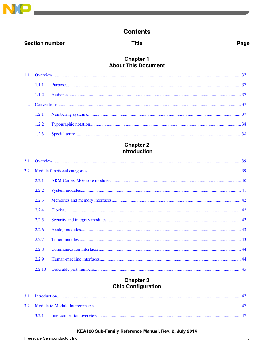
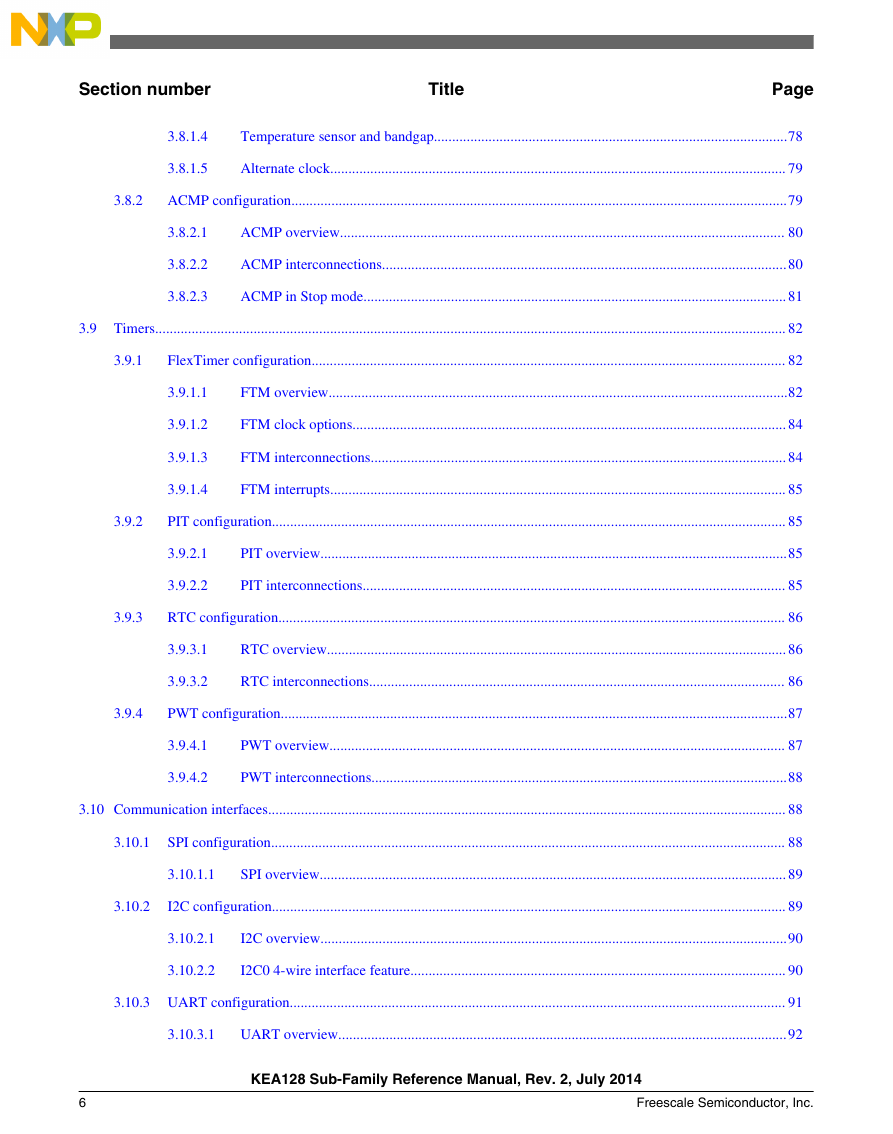
Section number Contents Title Chapter 1 About This Document Page 1.1 Overview.........................................................................................................................................................................37 1.1.1 Purpose.............................................................................................................................................................37 1.1.2 Audience.......................................................................................................................................................... 37 1.2 Conventions.................................................................................................................................................................... 37 1.2.1 Numbering systems..........................................................................................................................................37 1.2.2 Typographic notation....................................................................................................................................... 38 1.2.3 Special terms.................................................................................................................................................... 38 Chapter 2 Introduction 2.1 Overview.........................................................................................................................................................................39 2.2 Module functional categories..........................................................................................................................................39 2.2.1 ARM Cortex-M0+ core modules..................................................................................................................... 40 2.2.2 System modules............................................................................................................................................... 41 2.2.3 Memories and memory interfaces....................................................................................................................42 2.2.4 Clocks...............................................................................................................................................................42 2.2.5 Security and integrity modules........................................................................................................................ 42 2.2.6 Analog modules............................................................................................................................................... 43 2.2.7 Timer modules................................................................................................................................................. 43 2.2.8 Communication interfaces............................................................................................................................... 44 2.2.9 Human-machine interfaces.............................................................................................................................. 44 2.2.10 Orderable part numbers....................................................................................................................................45 Chapter 3 Chip Configuration 3.1 Introduction.....................................................................................................................................................................47 3.2 Module to Module Interconnects.................................................................................................................................... 47 3.2.1 Interconnection overview.................................................................................................................................47 Freescale Semiconductor, Inc. 3 KEA128 Sub-Family Reference Manual, Rev. 2, July 2014
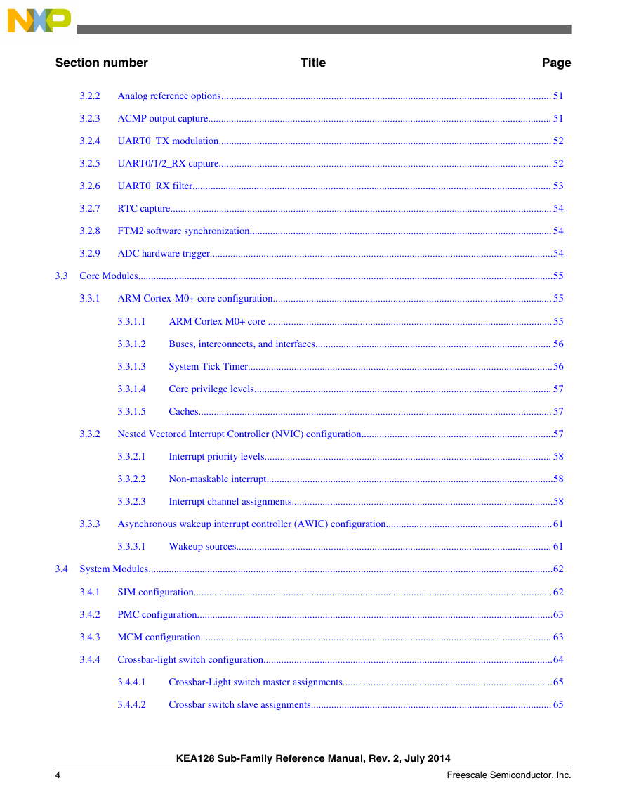
Section number Title Page 3.2.2 Analog reference options................................................................................................................................. 51 3.2.3 ACMP output capture...................................................................................................................................... 51 3.2.4 UART0_TX modulation.................................................................................................................................. 52 3.2.5 UART0/1/2_RX capture.................................................................................................................................. 52 3.2.6 UART0_RX filter............................................................................................................................................ 53 3.2.7 RTC capture..................................................................................................................................................... 54 3.2.8 FTM2 software synchronization...................................................................................................................... 54 3.2.9 ADC hardware trigger......................................................................................................................................54 3.3 Core Modules..................................................................................................................................................................55 3.3.1 ARM Cortex-M0+ core configuration............................................................................................................. 55 3.3.1.1 ARM Cortex M0+ core ............................................................................................................... 55 3.3.1.2 Buses, interconnects, and interfaces............................................................................................ 56 3.3.1.3 System Tick Timer.......................................................................................................................56 3.3.1.4 Core privilege levels.................................................................................................................... 57 3.3.1.5 Caches.......................................................................................................................................... 57 3.3.2 Nested Vectored Interrupt Controller (NVIC) configuration...........................................................................57 3.3.2.1 Interrupt priority levels................................................................................................................ 58 3.3.2.2 Non-maskable interrupt................................................................................................................58 3.3.2.3 Interrupt channel assignments......................................................................................................58 3.3.3 Asynchronous wakeup interrupt controller (AWIC) configuration.................................................................61 3.3.3.1 Wakeup sources........................................................................................................................... 61 3.4 System Modules..............................................................................................................................................................62 3.4.1 SIM configuration............................................................................................................................................ 62 3.4.2 PMC configuration...........................................................................................................................................63 3.4.3 MCM configuration......................................................................................................................................... 63 3.4.4 Crossbar-light switch configuration.................................................................................................................64 3.4.4.1 Crossbar-Light switch master assignments..................................................................................65 3.4.4.2 Crossbar switch slave assignments.............................................................................................. 65 4 Freescale Semiconductor, Inc. KEA128 Sub-Family Reference Manual, Rev. 2, July 2014
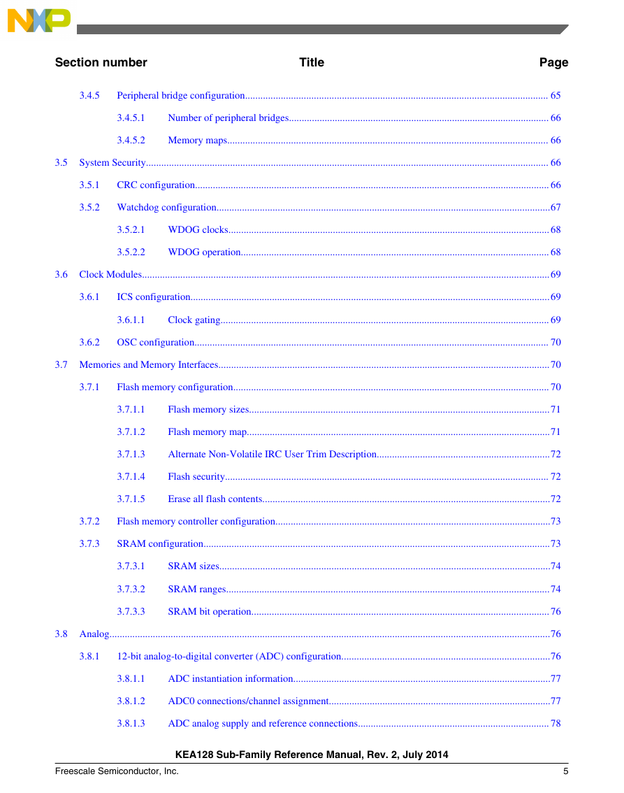
Section number Title Page 3.4.5 Peripheral bridge configuration....................................................................................................................... 65 3.4.5.1 Number of peripheral bridges...................................................................................................... 66 3.4.5.2 Memory maps.............................................................................................................................. 66 3.5 System Security.............................................................................................................................................................. 66 3.5.1 CRC configuration........................................................................................................................................... 66 3.5.2 Watchdog configuration...................................................................................................................................67 3.5.2.1 WDOG clocks.............................................................................................................................. 68 3.5.2.2 WDOG operation......................................................................................................................... 68 3.6 Clock Modules................................................................................................................................................................69 3.6.1 ICS configuration.............................................................................................................................................69 3.6.1.1 Clock gating................................................................................................................................. 69 3.6.2 OSC configuration........................................................................................................................................... 70 3.7 Memories and Memory Interfaces.................................................................................................................................. 70 3.7.1 Flash memory configuration............................................................................................................................ 70 3.7.1.1 Flash memory sizes......................................................................................................................71 3.7.1.2 Flash memory map.......................................................................................................................71 3.7.1.3 Alternate Non-Volatile IRC User Trim Description....................................................................72 3.7.1.4 Flash security............................................................................................................................... 72 3.7.1.5 Erase all flash contents.................................................................................................................72 3.7.2 Flash memory controller configuration............................................................................................................73 3.7.3 SRAM configuration........................................................................................................................................73 3.7.3.1 SRAM sizes..................................................................................................................................74 3.7.3.2 SRAM ranges...............................................................................................................................74 3.7.3.3 SRAM bit operation..................................................................................................................... 76 3.8 Analog.............................................................................................................................................................................76 3.8.1 12-bit analog-to-digital converter (ADC) configuration..................................................................................76 3.8.1.1 ADC instantiation information.....................................................................................................77 3.8.1.2 ADC0 connections/channel assignment.......................................................................................77 3.8.1.3 ADC analog supply and reference connections........................................................................... 78 Freescale Semiconductor, Inc. 5 KEA128 Sub-Family Reference Manual, Rev. 2, July 2014
Section number Title Page 3.8.1.4 Temperature sensor and bandgap.................................................................................................78 3.8.1.5 Alternate clock............................................................................................................................. 79 3.8.2 ACMP configuration........................................................................................................................................79 3.8.2.1 ACMP overview.......................................................................................................................... 80 3.8.2.2 ACMP interconnections...............................................................................................................80 3.8.2.3 ACMP in Stop mode.................................................................................................................... 81 3.9 Timers............................................................................................................................................................................. 82 3.9.1 FlexTimer configuration.................................................................................................................................. 82 3.9.1.1 FTM overview..............................................................................................................................82 3.9.1.2 FTM clock options....................................................................................................................... 84 3.9.1.3 FTM interconnections.................................................................................................................. 84 3.9.1.4 FTM interrupts............................................................................................................................. 85 3.9.2 PIT configuration............................................................................................................................................. 85 3.9.2.1 PIT overview................................................................................................................................85 3.9.2.2 PIT interconnections.................................................................................................................... 85 3.9.3 RTC configuration........................................................................................................................................... 86 3.9.3.1 RTC overview.............................................................................................................................. 86 3.9.3.2 RTC interconnections.................................................................................................................. 86 3.9.4 PWT configuration...........................................................................................................................................87 3.9.4.1 PWT overview............................................................................................................................. 87 3.9.4.2 PWT interconnections..................................................................................................................88 3.10 Communication interfaces.............................................................................................................................................. 88 3.10.1 SPI configuration............................................................................................................................................. 88 3.10.1.1 SPI overview................................................................................................................................ 89 3.10.2 I2C configuration............................................................................................................................................. 89 3.10.2.1 I2C overview................................................................................................................................90 3.10.2.2 I2C0 4-wire interface feature....................................................................................................... 90 3.10.3 UART configuration........................................................................................................................................ 91 3.10.3.1 UART overview...........................................................................................................................92 6 Freescale Semiconductor, Inc. KEA128 Sub-Family Reference Manual, Rev. 2, July 2014
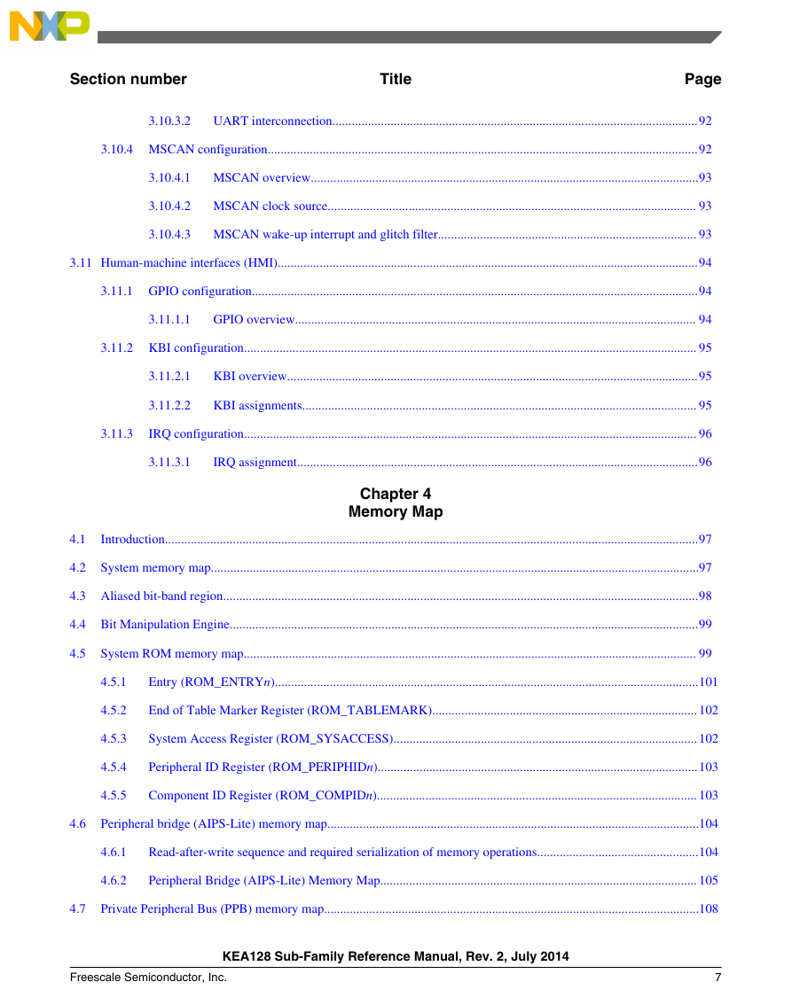
Section number Title Page 3.10.3.2 UART interconnection.................................................................................................................92 3.10.4 MSCAN configuration.....................................................................................................................................92 3.10.4.1 MSCAN overview........................................................................................................................93 3.10.4.2 MSCAN clock source.................................................................................................................. 93 3.10.4.3 MSCAN wake-up interrupt and glitch filter................................................................................ 93 3.11 Human-machine interfaces (HMI)..................................................................................................................................94 3.11.1 GPIO configuration..........................................................................................................................................94 3.11.1.1 GPIO overview............................................................................................................................ 94 3.11.2 KBI configuration............................................................................................................................................ 95 3.11.2.1 KBI overview...............................................................................................................................95 3.11.2.2 KBI assignments.......................................................................................................................... 95 3.11.3 IRQ configuration............................................................................................................................................ 96 3.11.3.1 IRQ assignment............................................................................................................................96 Chapter 4 Memory Map 4.1 Introduction.....................................................................................................................................................................97 4.2 System memory map.......................................................................................................................................................97 4.3 Aliased bit-band region...................................................................................................................................................98 4.4 Bit Manipulation Engine.................................................................................................................................................99 4.5 System ROM memory map............................................................................................................................................ 99 4.5.1 Entry (ROM_ENTRYn)...................................................................................................................................101 4.5.2 End of Table Marker Register (ROM_TABLEMARK).................................................................................. 102 4.5.3 System Access Register (ROM_SYSACCESS).............................................................................................. 102 4.5.4 Peripheral ID Register (ROM_PERIPHIDn)...................................................................................................103 4.5.5 Component ID Register (ROM_COMPIDn)................................................................................................... 103 4.6 Peripheral bridge (AIPS-Lite) memory map...................................................................................................................104 4.6.1 Read-after-write sequence and required serialization of memory operations..................................................104 4.6.2 Peripheral Bridge (AIPS-Lite) Memory Map.................................................................................................. 105 4.7 Private Peripheral Bus (PPB) memory map....................................................................................................................108 Freescale Semiconductor, Inc. 7 KEA128 Sub-Family Reference Manual, Rev. 2, July 2014
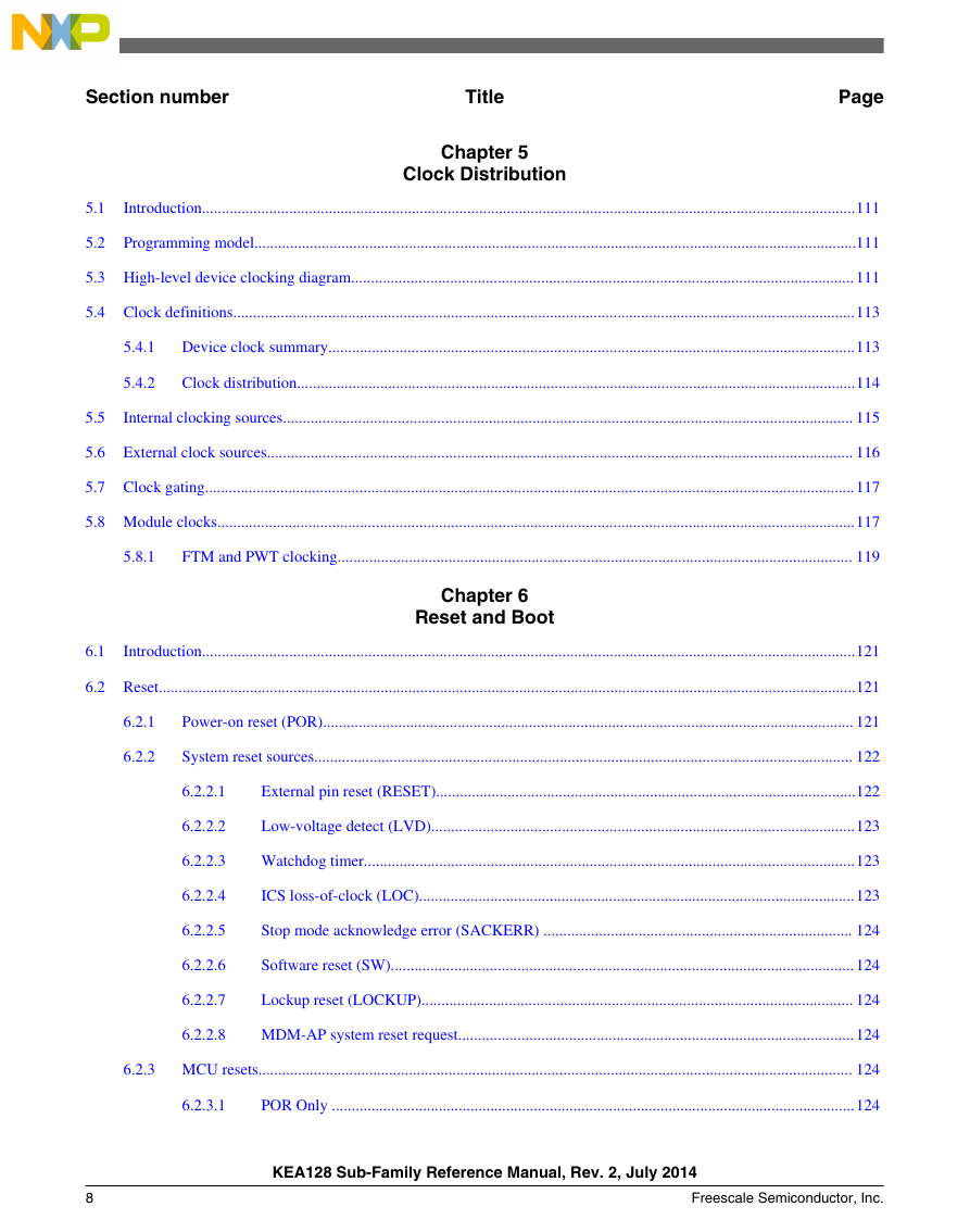
Section number Title Page Chapter 5 Clock Distribution 5.1 Introduction.....................................................................................................................................................................111 5.2 Programming model........................................................................................................................................................111 5.3 High-level device clocking diagram............................................................................................................................... 111 5.4 Clock definitions.............................................................................................................................................................113 5.4.1 Device clock summary.....................................................................................................................................113 5.4.2 Clock distribution.............................................................................................................................................114 5.5 Internal clocking sources................................................................................................................................................ 115 5.6 External clock sources.................................................................................................................................................... 116 5.7 Clock gating....................................................................................................................................................................117 5.8 Module clocks.................................................................................................................................................................117 5.8.1 FTM and PWT clocking.................................................................................................................................. 119 Chapter 6 Reset and Boot 6.1 Introduction.....................................................................................................................................................................121 6.2 Reset................................................................................................................................................................................121 6.2.1 Power-on reset (POR)...................................................................................................................................... 121 6.2.2 System reset sources........................................................................................................................................ 122 6.2.2.1 External pin reset (RESET)..........................................................................................................122 6.2.2.2 Low-voltage detect (LVD)...........................................................................................................123 6.2.2.3 Watchdog timer............................................................................................................................123 6.2.2.4 ICS loss-of-clock (LOC)..............................................................................................................123 6.2.2.5 Stop mode acknowledge error (SACKERR) .............................................................................. 124 6.2.2.6 Software reset (SW)..................................................................................................................... 124 6.2.2.7 Lockup reset (LOCKUP)............................................................................................................. 124 6.2.2.8 MDM-AP system reset request.................................................................................................... 124 6.2.3 MCU resets...................................................................................................................................................... 124 6.2.3.1 POR Only ....................................................................................................................................124 8 Freescale Semiconductor, Inc. KEA128 Sub-Family Reference Manual, Rev. 2, July 2014
分享到:
收藏