General Description:
JX-H62 is an HD CMOS image sensor designed with a
superior 3.0µm pixel with excellent low-light sensitivity and
low dark current performance. It features a 30fps native high
definition (HD) 720p video capability for camera applications
in PC multimedia, security, and entertainment devices.
The JX-H62 consists of a 1296x732 active pixel sensor (APS)
array with an on-chip 10-bit ADC, programmable gain control
(PGA), and correlated double sampling (CDS) to significantly
reduce fixed pattern noise (FPN). The sensor also has many
standard programmable and automatic functions. It has both
the industry compliant DVP parallel and MIPI CSI2 serial
interfaces. The external host controller can access this
device through a standard serial interface.
It is available in wafer-level packaged CSP.
Features :
• Automatic functions:
o AEC – Automatic Exposure Control
o AGC – Automatic Gain Control
o ABLC – Automatic Black Level Calibration
• Programmable controls:
o Gain, exposure, frame rate and size
o Image mirror and flip
o Window panning and cropping
o I2C slave ID
• Output formats:
o DVP parallel interface
o MIPI CSI2 1 Lane
• Data formats:
o 10-bit RAW RGB
• Others
o 50/60Hz flick noise cancellation
o Register group write capability
o Frame synchronization
o Black sun spot cancellation
Confidential and Proprietary
JX-H62: HD CMOS Image Sensor
With MIPI Interface
Key Specifications:
Optical format
Active Pixels
Pixel size
Color filter array
Chief Ray Angle
Shutter type
1/4”
1296H x 732V
3.0 x 3.0 µm
RGB Bayer pattern
17.5 degrees linear
Electronic rolling shutter
Maximum Frame Rate
30fps
Digital
1.35 – 1.65V (1.5V nominal)
Supply voltage
Analog
2.6 – 3.0V (2.8V nominal)
I/O
1.7 – 3.0V (1.8V nominal)
Power
consumption
Active
42mA
Standby
< 300 µA
Output Formats
Sensitivity
Max SNR
Dynamic Range
Dark Current
Operating
junction temperature
Stable image
junction temperature
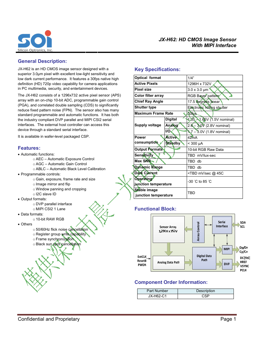
Functional Block:
10-bit RGB Raw Data
TBD mV/lux-sec
TBD db
TBD db
JX-H62: HD CMOS Image Sensor
With MIPI Interface
Contents
Pin Diagram:............................................................................................................................................................ 3
Functional Overview:............................................................................................................................................... 5
Pixel Array Format: .................................................................................................................................................. 6
Data Output Format: ............................................................................................................................................... 7
Sensor Luminance Control: ...................................................................................................................................... 8
Test Pattern Output:................................................................................................................................................ 8
MIPI interface:......................................................................................................................................................... 9
Frame Synchronization: ........................................................................................................................................... 9
Serial Interface: ..................................................................................................................................................... 10
Register Group Write Function: ............................................................................................................................. 11
Power on/off sequence: ........................................................................................................................................ 12
Electrical Characteristics: ....................................................................................................................................... 14
CRA Specifications: ................................................................................................................................................ 15
Mechanical Specifications:..................................................................................................................................... 16
CSP Module Schematic (Reference): ...................................................................................................................... 18
Register Descriptions:............................................................................................................................................ 20
Document Revision Control ................................................................................................................................... 25
Confidential and Proprietary
Page 2
�
JX-H62: HD CMOS Image Sensor
With MIPI Interface
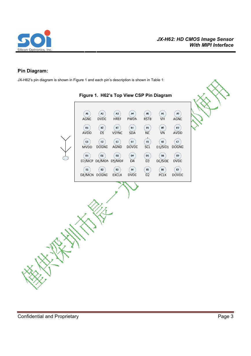
Pin Diagram:
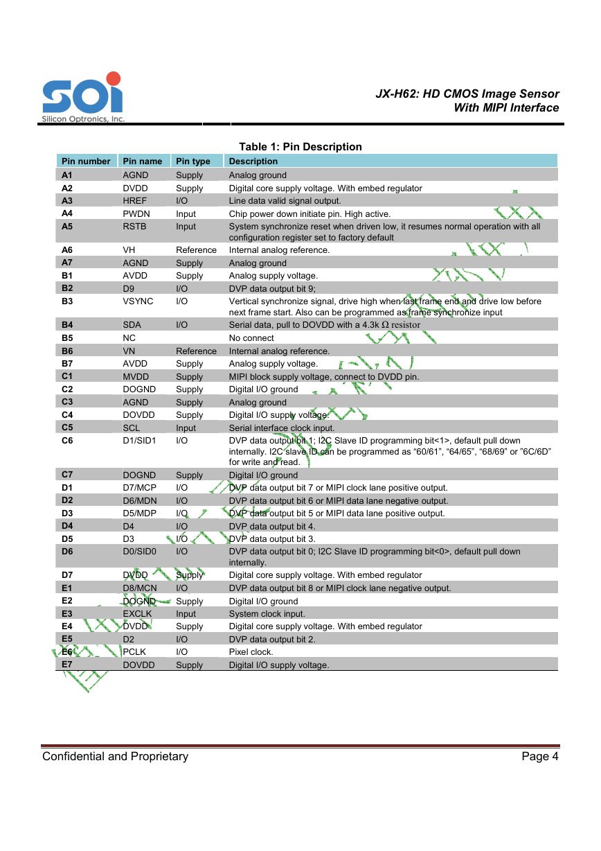
JX-H62’s pin diagram is shown in Figure 1 and each pin’s description is shown in Table 1:
Figure 1. H62’s Top View CSP Pin Diagram
Confidential and Proprietary
Page 3
�
JX-H62: HD CMOS Image Sensor
With MIPI Interface
Pin number Pin name Pin type
Description
Table 1: Pin Description
A1
A2
A3
A4
A5
A6
A7
B1
B2
B3
B4
B5
B6
B7
C1
C2
C3
C4
C5
C6
C7
D1
D2
D3
D4
D5
D6
D7
E1
E2
E3
E4
E5
E6
E7
AGND
DVDD
HREF
PWDN
RSTB
VH
AGND
AVDD
D9
VSYNC
SDA
NC
VN
AVDD
MVDD
DOGND
AGND
DOVDD
SCL
Supply
Supply
I/O
Input
Input
Analog ground
Digital core supply voltage. With embed regulator
Line data valid signal output.
Chip power down initiate pin. High active.
System synchronize reset when driven low, it resumes normal operation with all
configuration register set to factory default
Reference
Internal analog reference.
Supply
Supply
I/O
I/O
I/O
Analog ground
Analog supply voltage.
DVP data output bit 9;
Vertical synchronize signal, drive high when last frame end and drive low before
next frame start. Also can be programmed as frame synchronize input
Serial data, pull to DOVDD with a 4.3k Ω resistor
No connect
Reference
Internal analog reference.
Supply
Supply
Supply
Supply
Supply
Input
Analog supply voltage.
MIPI block supply voltage, connect to DVDD pin.
Digital I/O ground
Analog ground
Digital I/O supply voltage.
Serial interface clock input.
D1/SID1
I/O
DVP data output bit 1; I2C Slave ID programming bit<1>, default pull down
internally. I2C slave ID can be programmed as “60/61”, “64/65”, “68/69” or ”6C/6D”
for write and read.
DOGND
Supply
Digital I/O ground
D7/MCP
D6/MDN
D5/MDP
D4
D3
D0/SID0
I/O
I/O
I/O
I/O
I/O
I/O
DVP data output bit 7 or MIPI clock lane positive output.
DVP data output bit 6 or MIPI data lane negative output.
DVP data output bit 5 or MIPI data lane positive output.
DVP data output bit 4.
DVP data output bit 3.
DVP data output bit 0; I2C Slave ID programming bit<0>, default pull down
internally.
DVDD
Supply
Digital core supply voltage. With embed regulator
D8/MCN
I/O
DVP data output bit 8 or MIPI clock lane negative output.
DOGND
Supply
Digital I/O ground
EXCLK
DVDD
D2
PCLK
Input
Supply
I/O
I/O
System clock input.
Digital core supply voltage. With embed regulator
DVP data output bit 2.
Pixel clock.
DOVDD
Supply
Digital I/O supply voltage.
Confidential and Proprietary
Page 4
�
JX-H62: HD CMOS Image Sensor
With MIPI Interface
Functional Overview:
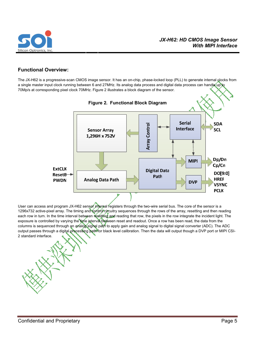
The JX-H62 is a progressive-scan CMOS image sensor. It has an on-chip, phase-locked loop (PLL) to generate internal clocks from
a single master input clock running between 6 and 27MHz. Its analog data process and digital data process can handle up to
70Mp/s at corresponding pixel clock 70MHz. Figure 2 illustrates a block diagram of the sensor.
Figure 2. Functional Block Diagram
User can access and program JX-H62 sensor internal registers through the two-wire serial bus. The core of the sensor is a
1296x732 active-pixel array. The timing and control circuitry sequences through the rows of the array, resetting and then reading
each row in turn. In the time interval between resetting and reading that row, the pixels in the row integrate the incident light. The
exposure is controlled by varying the time interval between reset and readout. Once a row has been read, the data from the
columns is sequenced through an analog signal path to apply gain and analog signal to digital signal converter (ADC). The ADC
output passes through a digital processing path for black level calibration. Then the data will output though a DVP port or MIPI CSI-
2 standard interface.
Confidential and Proprietary
Page 5
�
JX-H62: HD CMOS Image Sensor
With MIPI Interface
Pixel Array Format:
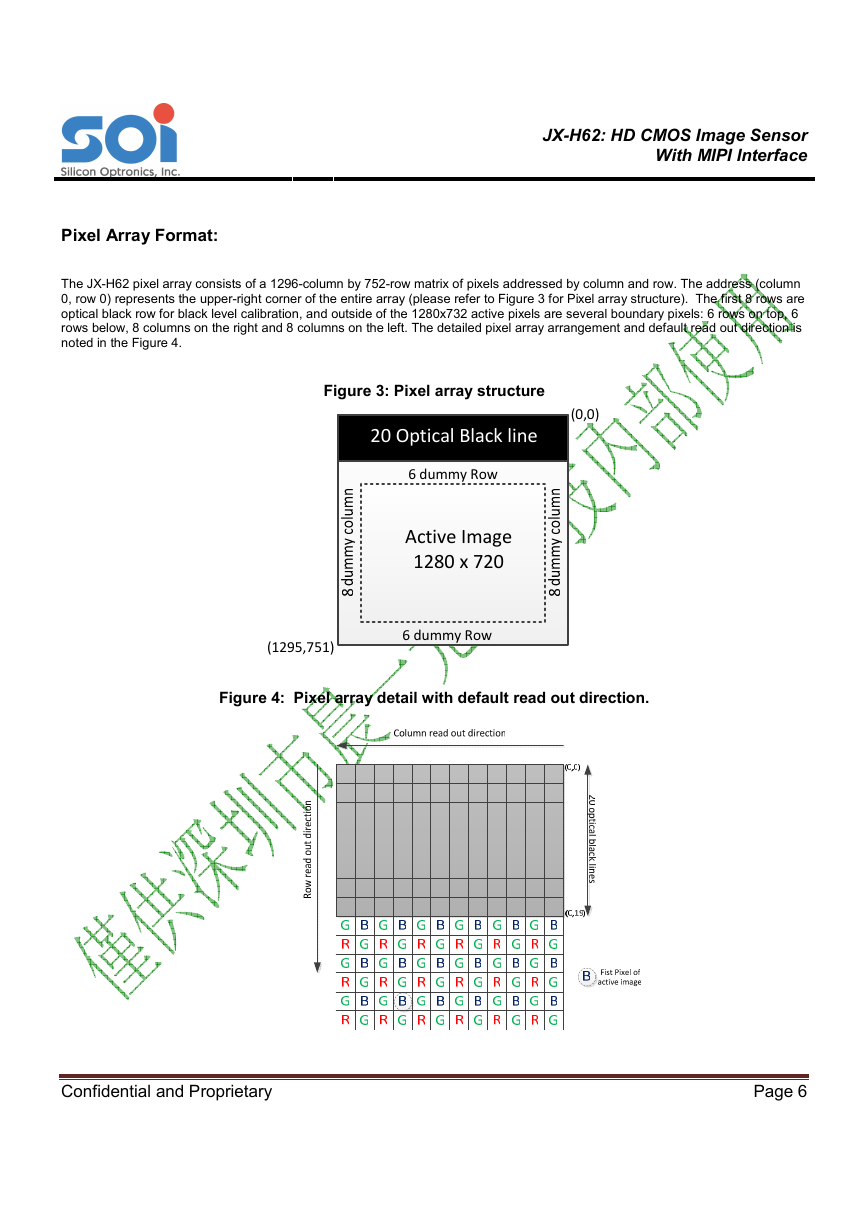
The JX-H62 pixel array consists of a 1296-column by 752-row matrix of pixels addressed by column and row. The address (column
0, row 0) represents the upper-right corner of the entire array (please refer to Figure 3 for Pixel array structure). The first 8 rows are
optical black row for black level calibration, and outside of the 1280x732 active pixels are several boundary pixels: 6 rows on top, 6
rows below, 8 columns on the right and 8 columns on the left. The detailed pixel array arrangement and default read out direction is
noted in the Figure 4.
Figure 3: Pixel array structure
(0,0)
20 Optical Black line
6 dummy Row
Active Image
1280 x 720
(1295,751)
6 dummy Row
Figure 4: Pixel array detail with default read out direction.
Confidential and Proprietary
Page 6
�
Data Output Format:
JX-H62: HD CMOS Image Sensor
With MIPI Interface
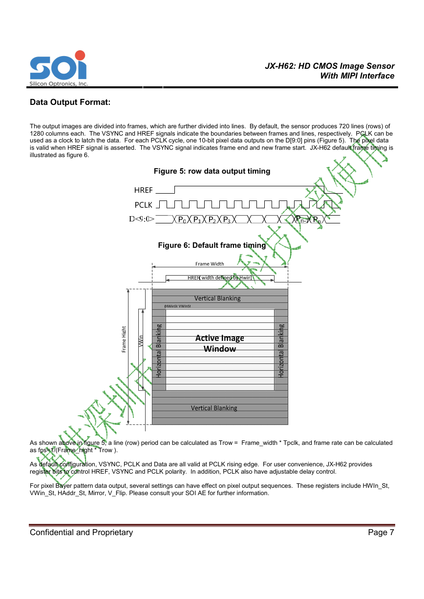
The output images are divided into frames, which are further divided into lines. By default, the sensor produces 720 lines (rows) of
1280 columns each. The VSYNC and HREF signals indicate the boundaries between frames and lines, respectively. PCLK can be
used as a clock to latch the data. For each PCLK cycle, one 10-bit pixel data outputs on the D[9:0] pins (Figure 5). The pixel data
is valid when HREF signal is asserted. The VSYNC signal indicates frame end and new frame start. JX-H62 default frame timing is
illustrated as figure 6.
Figure 5: row data output timing
Figure 6: Default frame timing
As shown above in figure 5, a line (row) period can be calculated as Trow = Frame_width * Tpclk, and frame rate can be calculated
as fps=1/(Frame_hight * Trow ).
As default configuration, VSYNC, PCLK and Data are all valid at PCLK rising edge. For user convenience, JX-H62 provides
register bits to control HREF, VSYNC and PCLK polarity. In addition, PCLK also have adjustable delay control.
For pixel Bayer pattern data output, several settings can have effect on pixel output sequences. These registers include HWIn_St,
VWin_St, HAddr_St, Mirror, V_Flip. Please consult your SOI AE for further information.
Confidential and Proprietary
Page 7
�
Sensor Luminance Control:
JX-H62: HD CMOS Image Sensor
With MIPI Interface
JX-H62 has built-in automatic luminance control capability. The main purpose for luminance control is to get proper image level
through exposure and gain adjustment. There are 2 configurations described below:
1) 50/60Hz flick noise cancelling (also known as banding filter). When this feature is turned on, user needs to set the line
equivalents of 1/100s or 1/120s, exposure will attempt to stay within n/100s or n/120s boundaries (where “n” is an integer
number). The gap between each step will be filled with gain. If the light is too strong, exposure will continuously adjust to
under 1/100s or 1/120 boundary conditions. Under this condition, the moving or fixed light bands may still be observed by user.
2) Auto frame rate adjustment. For some extreme low light condition, JX-H62 provides the option to automatically slow down the
frame rate to adjust exposure to a proper image level. The lowest frame rate is 1/8.
Test Pattern Output:
JX-H62 can output test patterns as described below:
1) Walking “1” test pattern: for most sensor module connectivity test, JX-H62 provides walking “1” test pattern.
Confidential and Proprietary
Page 8
�



 2023年江西萍乡中考道德与法治真题及答案.doc
 2012年重庆南川中考生物真题及答案.doc
 2013年江西师范大学地理学综合及文艺理论基础考研真题.doc
 2020年四川甘孜小升初语文真题及答案I卷.doc
 2020年注册岩土工程师专业基础考试真题及答案.doc
 2023-2024学年福建省厦门市九年级上学期数学月考试题及答案.doc
 2021-2022学年辽宁省沈阳市大东区九年级上学期语文期末试题及答案.doc
 2022-2023学年北京东城区初三第一学期物理期末试卷及答案.doc
 2018上半年江西教师资格初中地理学科知识与教学能力真题及答案.doc
 2012年河北国家公务员申论考试真题及答案-省级.doc
 2020-2021学年江苏省扬州市江都区邵樊片九年级上学期数学第一次质量检测试题及答案.doc
 2022下半年黑龙江教师资格证中学综合素质真题及答案.doc