Microwave Wideband Synthesizer
with Integrated VCO
ADF5355
GENERAL DESCRIPTION
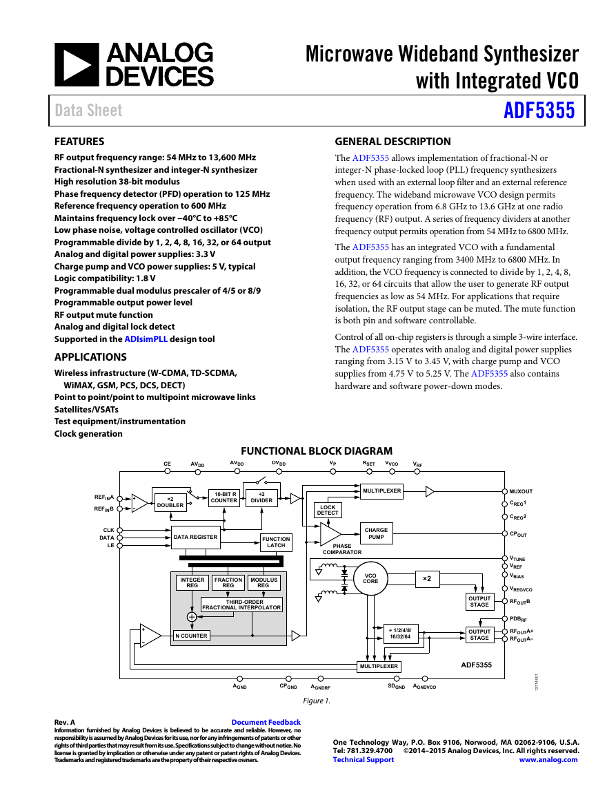
The ADF5355 allows implementation of fractional-N or
integer-N phase-locked loop (PLL) frequency synthesizers
when used with an external loop filter and an external reference
frequency. The wideband microwave VCO design permits
frequency operation from 6.8 GHz to 13.6 GHz at one radio
frequency (RF) output. A series of frequency dividers at another
frequency output permits operation from 54 MHz to 6800 MHz.
The ADF5355 has an integrated VCO with a fundamental
output frequency ranging from 3400 MHz to 6800 MHz. In
addition, the VCO frequency is connected to divide by 1, 2, 4, 8,
16, 32, or 64 circuits that allow the user to generate RF output
frequencies as low as 54 MHz. For applications that require
isolation, the RF output stage can be muted. The mute function
is both pin and software controllable.
Control of all on-chip registers is through a simple 3-wire interface.
The ADF5355 operates with analog and digital power supplies
ranging from 3.15 V to 3.45 V, with charge pump and VCO
supplies from 4.75 V to 5.25 V. The ADF5355 also contains
hardware and software power-down modes.
Data Sheet
FEATURES
RF output frequency range: 54 MHz to 13,600 MHz
Fractional-N synthesizer and integer-N synthesizer
High resolution 38-bit modulus
Phase frequency detector (PFD) operation to 125 MHz
Reference frequency operation to 600 MHz
Maintains frequency lock over −40°C to +85°C
Low phase noise, voltage controlled oscillator (VCO)
Programmable divide by 1, 2, 4, 8, 16, 32, or 64 output
Analog and digital power supplies: 3.3 V
Charge pump and VCO power supplies: 5 V, typical
Logic compatibility: 1.8 V
Programmable dual modulus prescaler of 4/5 or 8/9
Programmable output power level
RF output mute function
Analog and digital lock detect
Supported in the ADIsimPLL design tool
APPLICATIONS
Wireless infrastructure (W-CDMA, TD-SCDMA,
WiMAX, GSM, PCS, DCS, DECT)
Point to point/point to multipoint microwave links
Satellites/VSATs
Test equipment/instrumentation
Clock generation
CE
AVDD
FUNCTIONAL BLOCK DIAGRAM
VVCO
DVDD
AVDD
VP
RSET
VRF
REFINA
B
REFIN
CLK
DATA
LE
×2
DOUBLER
10-BIT R
COUNTER
÷2
DIVIDER
DATA REGISTER
FUNCTION
LATCH
INTEGER
REG
FRACTION
REG
MODULUS
REG
THIRD-ORDER
FRACTIONAL INTERPOLATOR
MULTIPLEXER
LOCK
DETECT
CHARGE
PUMP
PHASE
COMPARATOR
VCO
CORE
×2
N COUNTER
÷ 1/2/4/8/
16/32/64
OUTPUT
STAGE
OUTPUT
STAGE
MULTIPLEXER
ADF5355
AGND
CPGND
AGNDRF
SDGND
AGNDVCO
Figure 1.
MUXOUT
CREG1
CREG2
CPOUT
VTUNE
VREF
VBIAS
VREGVCO
RFOUTB
PDBRF
RFOUTA+
RFOUTA–
1
0
0
-
4
1
7
2
1
Rev. A
Document Feedback
Information furnished by Analog Devices is believed to be accurate and reliable. However, no
responsibility is assumed by Analog Devices for its use, nor for any infringements of patents or other
rights of third parties that may result from its use. Specifications subject to change without notice. No
license is granted by implication or otherwise under any patent or patent rights of Analog Devices.
Trademarks and registered trademarks are the property of their respective owners.
One Technology Way, P.O. Box 9106, Norwood, MA 02062-9106, U.S.A.
Tel: 781.329.4700 ©2014–2015 Analog Devices, Inc. All rights reserved.
Technical Support
www.analog.com
�
ADF5355
TABLE OF CONTENTS
Features .............................................................................................. 1
Applications ....................................................................................... 1
General Description ......................................................................... 1
Functional Block Diagram .............................................................. 1
Revision History ............................................................................... 3
Specifications ..................................................................................... 4
Timing Characteristics ................................................................ 7
Absolute Maximum Ratings ............................................................ 8
Transistor Count ........................................................................... 8
ESD Caution .................................................................................. 8
Pin Configuration and Function Descriptions ............................. 9
Typical Performance Characteristics ........................................... 11
Circuit Description ......................................................................... 16
Reference Input ........................................................................... 16
RF N Divider ............................................................................... 16
Phase Frequency Detector (PFD) and Charge Pump ............ 17
MUXOUT and Lock Detect ...................................................... 17
Input Shift Registers ................................................................... 17
Program Modes .......................................................................... 18
VCO.............................................................................................. 18
Output Stage ................................................................................ 18
Register Maps .................................................................................. 20
Register 0 ..................................................................................... 22
Register 1 ..................................................................................... 23
Register 2 ..................................................................................... 24
Data Sheet
Register 3 ..................................................................................... 25
Register 4 ..................................................................................... 26
Register 5 ..................................................................................... 27
Register 6 ..................................................................................... 28
Register 7 ..................................................................................... 30
Register 8 ..................................................................................... 31
Register 9 ..................................................................................... 31
Register 10 ................................................................................... 32
Register 11 ................................................................................... 32
Register 12 ................................................................................... 33
Register Initialization Sequence ............................................... 33
Frequency Update Sequence ..................................................... 33
RF Synthesizer—A Worked Example ...................................... 34
Reference Doubler and Reference Divider ............................. 34
Spurious Optimization and Fast Lock ..................................... 34
Optimizing Jitter ......................................................................... 34
Spur Mechanisms ....................................................................... 35
Lock Time.................................................................................... 35
Applications Information .............................................................. 36
Power Supplies ............................................................................ 36
Printed Circuit Board (PCB) Design Guidelines for a
Chip-Scale Package .................................................................... 36
Output Matching ........................................................................ 37
Outline Dimensions ....................................................................... 38
Ordering Guide .......................................................................... 38
Rev. A | Page 2 of 38
�
Data Sheet
REVISION HISTORY
2/15—Rev. 0 to Rev. A
Changed Register 5, Bit DB5 Value from 0 to 1 ........ Throughout
Changed Register 5 Default Value from 0x00800005 to
0x00800025 .................................................................... Throughout
Changed Register 8 Default Value from 0x102D4028 to
0x102D0428 ................................................................... Throughout
Changes to Table 1 ............................................................................ 4
Changed Timing Diagram Section to Write Timing Diagram
Section ................................................................................................ 7
Changes to Table 4 .......................................................................... 10
Changes to Figure 4 to Figure 6 .................................................... 11
Added Figure 7 to Figure 9; Renumbered Sequentially ............. 11
Changes to Figure 10 to Figure 18 ................................................ 12
Changes to Figure 20 ...................................................................... 13
Changes to Figure 23 and Figure 27 ............................................. 14
Changes to Figure 28 to Figure 30 and Figure 31 Caption ........ 15
Changes to Reference Input Section and INT, FRAC, MOD,
and R Counter Relationship Section ............................................ 16
Changes to Phase Frequency Detector (PFD) and Charge Pump
Section .............................................................................................. 17
Changes to VCO Section and Output Stage Section .................. 18
ADF5355
Changes to Automatic Calibration (AUTOCAL) Section ......... 22
Changes to Figure 43 ...................................................................... 24
Changes to MUXOUT Section ...................................................... 26
Changes to Reference Mode Section and Counter Reset
Section .............................................................................................. 27
Changes to Negative Bleed Section ............................................... 28
Changes to Charge Pump Bleed Current Section ....................... 29
Changes to Register 9 Section, VCO Band Division Section,
Timeout Section, Automatic Level Calibration Timeout Section,
and Synthesizer Lock Timeout Section ........................................ 31
Changes to ADC Conversion Clock (ADC_CLK_DIV)
Section .............................................................................................. 32
Changes to Phase Resync Clock Divider Value Section and
Frequency Update Sequence Section............................................ 33
Changes to RF Synthesizer—A Worked Example Section ........ 34
Changes to Lock Time Section and Automatic Level
Calibration Timeout Section ......................................................... 35
Added Lock Time—A Worked Example Section ....................... 35
10/14—Revision 0: Initial Version
Rev. A | Page 3 of 38
�
ADF5355
Data Sheet
SPECIFICATIONS
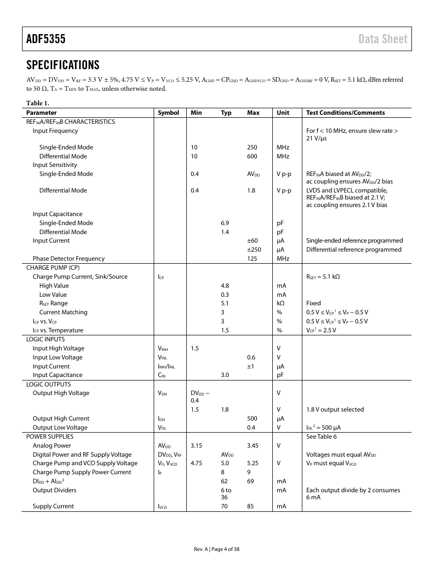
AVDD = DVDD = VRF = 3.3 V ± 5%, 4.75 V ≤ VP = VVCO ≤ 5.25 V, AGND = CPGND = AGNDVCO = SDGND = AGNDRF = 0 V, RSET = 5.1 kΩ, dBm referred
to 50 Ω, TA = TMIN to TMAX, unless otherwise noted.
Symbol Min
Typ
Max
Unit
Test Conditions/Comments
Table 1.
Parameter
REFINA/REFINB CHARACTERISTICS
Input Frequency
Single-Ended Mode
Differential Mode
Input Sensitivity
Single-Ended Mode
Differential Mode
Input Capacitance
Single-Ended Mode
Differential Mode
Input Current
Phase Detector Frequency
CHARGE PUMP (CP)
Charge Pump Current, Sink/Source
ICP
High Value
Low Value
RSET Range
Current Matching
ICP vs. VCP
ICP vs. Temperature
LOGIC INPUTS
Input High Voltage
Input Low Voltage
Input Current
Input Capacitance
LOGIC OUTPUTS
Output High Voltage
Output High Current
Output Low Voltage
POWER SUPPLIES
Analog Power
Digital Power and RF Supply Voltage
Charge Pump and VCO Supply Voltage
Charge Pump Supply Power Current
DIDD + AIDD
Output Dividers
3
1.5
DVDD −
0.4
1.5
VINH
VINL
IINH/IINL
CIN
VOH
IOH
VOL
AVDD
DVDD, VRF
VP, VVCO
IP
3.15
4.75
Supply Current
IVCO
10
10
0.4
0.4
For f < 10 MHz, ensure slew rate >
21 V/µs
REFINA biased at AVDD/2;
ac coupling ensures AVDD/2 bias
LVDS and LVPECL compatible,
REFINA/REFINB biased at 2.1 V;
ac coupling ensures 2.1 V bias
Single-ended reference programmed
Differential reference programmed
250
600
MHz
MHz
AVDD
V p-p
1.8
V p-p
pF
pF
µA
µA
MHz
±60
±250
125
mA
mA
kΩ
%
%
%
V
V
µA
pF
V
V
µA
V
V
V
mA
mA
mA
0.6
±1
500
0.4
3.45
5.25
9
69
85
RSET = 5.1 kΩ
Fixed
0.5 V ≤ VCP
0.5 V ≤ VCP
VCP
1 = 2.5 V
1 ≤ VP − 0.5 V
1 ≤ VP − 0.5 V
1.8 V output selected
IOL
2 = 500 µA
See Table 6
Voltages must equal AVDD
VP must equal VVCO
Each output divide by 2 consumes
6 mA
6.9
1.4
4.8
0.3
5.1
3
3
1.5
3.0
1.8
AVDD
5.0
8
62
6 to
36
70
Rev. A | Page 4 of 38
�
Data Sheet
Parameter
RFOUTA±/RFOUTB Supply Current
Symbol Min
IRFOUTx±
Typ
Max
Unit
Low Power Sleep Mode
RF OUTPUT CHARACTERISTICS
VCO Frequency Range
RFOUTB Output Frequency
RFOUTA+/RFOUTA− Output Frequency
VCO Sensitivity
Frequency Pushing (Open-Loop)
Frequency Pulling (Open-Loop)
KV
Harmonic Content
Second
Third
Fundamental VCO Feedthrough
RF Output Power4
RF Output Power Variation
RF Output Power Variation (over Frequency)
Level of Signal with RF Output Disabled
NOISE CHARACTERISTICS
Fundamental VCO Phase Noise Performance
20
35
50
70
16
30
42
55
500
1000
3400
6800
53.125
6800
13600
6800
15
15
0.5
30
−27
−22
−20
−12
−8
−55
+8
−3
1
−1
±1
±1
±6
±4
−60
−30
−15
−17
−116
−136
−138
−155
−113
−133
−135
−153
−110
−130
−132
−150
Rev. A | Page 5 of 38
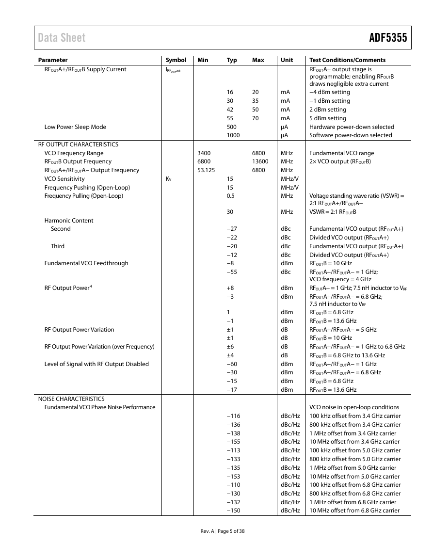
ADF5355
Test Conditions/Comments
RFOUTA± output stage is
programmable; enabling RFOUTB
draws negligible extra current
−4 dBm setting
−1 dBm setting
2 dBm setting
5 dBm setting
Hardware power-down selected
Software power-down selected
Fundamental VCO range
2× VCO output (RFOUTB)
Voltage standing wave ratio (VSWR) =
2:1 RFOUTA+/RFOUTA−
VSWR = 2:1 RFOUTB
Fundamental VCO output (RFOUTA+)
Divided VCO output (RFOUTA+)
Fundamental VCO output (RFOUTA+)
Divided VCO output (RFOUTA+)
RFOUTB = 10 GHz
RFOUTA+/RFOUTA− = 1 GHz;
VCO frequency = 4 GHz
RFOUTA+ = 1 GHz; 7.5 nH inductor to VRF
RFOUTA+/RFOUTA− = 6.8 GHz;
7.5 nH inductor to VRF
RFOUTB = 6.8 GHz
RFOUTB = 13.6 GHz
RFOUTA+/RFOUTA− = 5 GHz
RFOUTB = 10 GHz
RFOUTA+/RFOUTA− = 1 GHz to 6.8 GHz
RFOUTB = 6.8 GHz to 13.6 GHz
RFOUTA+/RFOUTA− = 1 GHz
RFOUTA+/RFOUTA− = 6.8 GHz
RFOUTB = 6.8 GHz
RFOUTB = 13.6 GHz
mA
mA
mA
mA
µA
µA
MHz
MHz
MHz
MHz/V
MHz/V
MHz
MHz
dBc
dBc
dBc
dBc
dBm
dBc
dBm
dBm
dBm
dBm
dB
dB
dB
dB
dBm
dBm
dBm
dBm
dBc/Hz
dBc/Hz
dBc/Hz
dBc/Hz
dBc/Hz
dBc/Hz
dBc/Hz
dBc/Hz
dBc/Hz
dBc/Hz
dBc/Hz
dBc/Hz
VCO noise in open-loop conditions
100 kHz offset from 3.4 GHz carrier
800 kHz offset from 3.4 GHz carrier
1 MHz offset from 3.4 GHz carrier
10 MHz offset from 3.4 GHz carrier
100 kHz offset from 5.0 GHz carrier
800 kHz offset from 5.0 GHz carrier
1 MHz offset from 5.0 GHz carrier
10 MHz offset from 5.0 GHz carrier
100 kHz offset from 6.8 GHz carrier
800 kHz offset from 6.8 GHz carrier
1 MHz offset from 6.8 GHz carrier
10 MHz offset from 6.8 GHz carrier
�
ADF5355
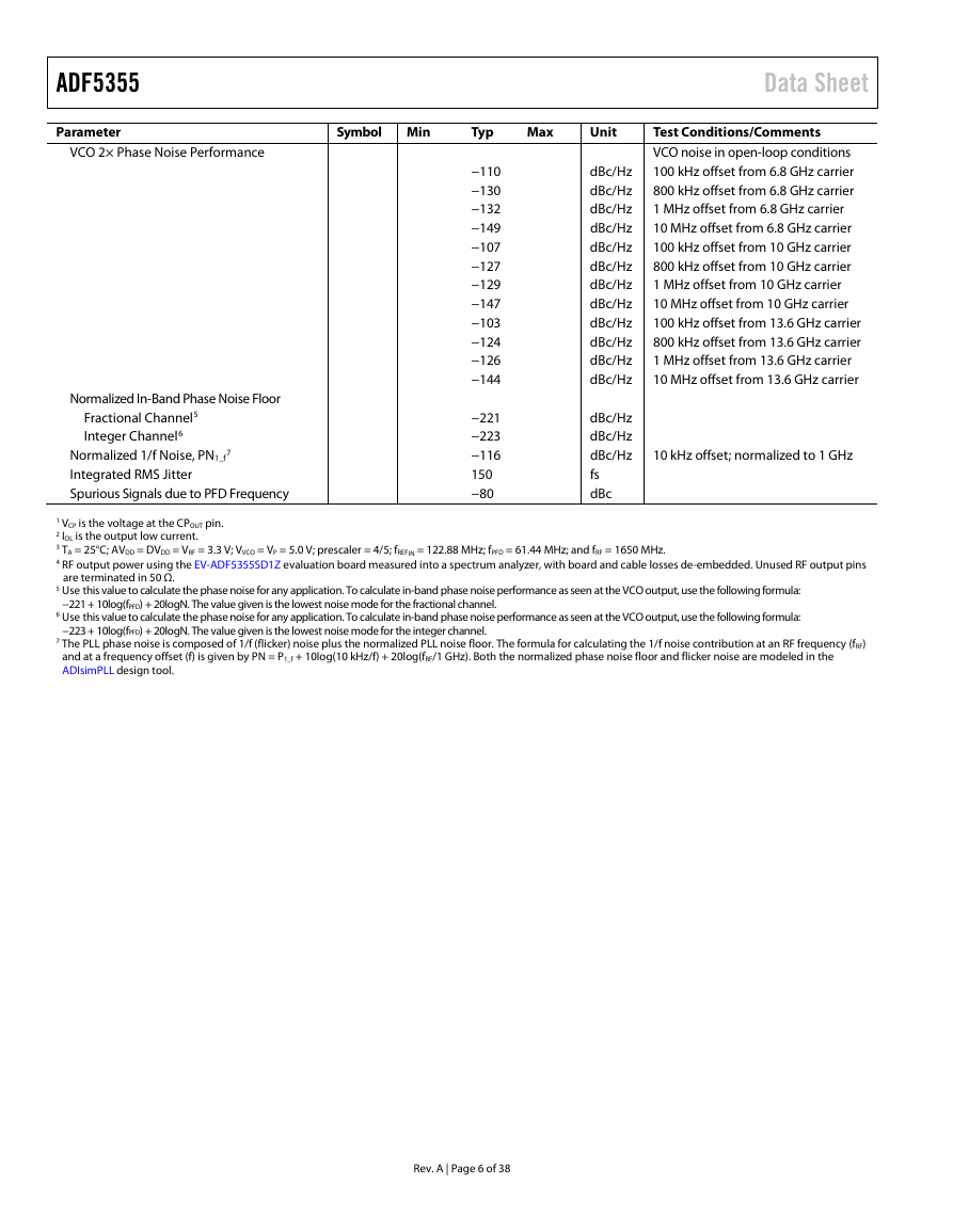
Parameter
VCO 2× Phase Noise Performance
Symbol Min
Typ
Max
Unit
−110
−130
−132
−149
−107
−127
−129
−147
−103
−124
−126
−144
−221
−223
−116
150
−80
dBc/Hz
dBc/Hz
dBc/Hz
dBc/Hz
dBc/Hz
dBc/Hz
dBc/Hz
dBc/Hz
dBc/Hz
dBc/Hz
dBc/Hz
dBc/Hz
dBc/Hz
dBc/Hz
dBc/Hz
fs
dBc
Normalized In-Band Phase Noise Floor
Fractional Channel5
Integer Channel6
Normalized 1/f Noise, PN1_f
Integrated RMS Jitter
Spurious Signals due to PFD Frequency
7
Data Sheet
Test Conditions/Comments
VCO noise in open-loop conditions
100 kHz offset from 6.8 GHz carrier
800 kHz offset from 6.8 GHz carrier
1 MHz offset from 6.8 GHz carrier
10 MHz offset from 6.8 GHz carrier
100 kHz offset from 10 GHz carrier
800 kHz offset from 10 GHz carrier
1 MHz offset from 10 GHz carrier
10 MHz offset from 10 GHz carrier
100 kHz offset from 13.6 GHz carrier
800 kHz offset from 13.6 GHz carrier
1 MHz offset from 13.6 GHz carrier
10 MHz offset from 13.6 GHz carrier
10 kHz offset; normalized to 1 GHz
1 VCP is the voltage at the CPOUT pin.
2 IOL is the output low current.
3 TA = 25°C; AVDD = DVDD = VRF = 3.3 V; VVCO = VP = 5.0 V; prescaler = 4/5; fREFIN = 122.88 MHz; fPFD = 61.44 MHz; and fRF = 1650 MHz.
4 RF output power using the EV-ADF5355SD1Z evaluation board measured into a spectrum analyzer, with board and cable losses de-embedded. Unused RF output pins
are terminated in 50 Ω.
5 Use this value to calculate the phase noise for any application. To calculate in-band phase noise performance as seen at the VCO output, use the following formula:
−221 + 10log(fPFD) + 20logN. The value given is the lowest noise mode for the fractional channel.
6 Use this value to calculate the phase noise for any application. To calculate in-band phase noise performance as seen at the VCO output, use the following formula:
−223 + 10log(fPFD) + 20logN. The value given is the lowest noise mode for the integer channel.
7 The PLL phase noise is composed of 1/f (flicker) noise plus the normalized PLL noise floor. The formula for calculating the 1/f noise contribution at an RF frequency (fRF)
and at a frequency offset (f) is given by PN = P1_f + 10log(10 kHz/f) + 20log(fRF/1 GHz). Both the normalized phase noise floor and flicker noise are modeled in the
ADIsimPLL design tool.
Rev. A | Page 6 of 38
�
Data Sheet
ADF5355
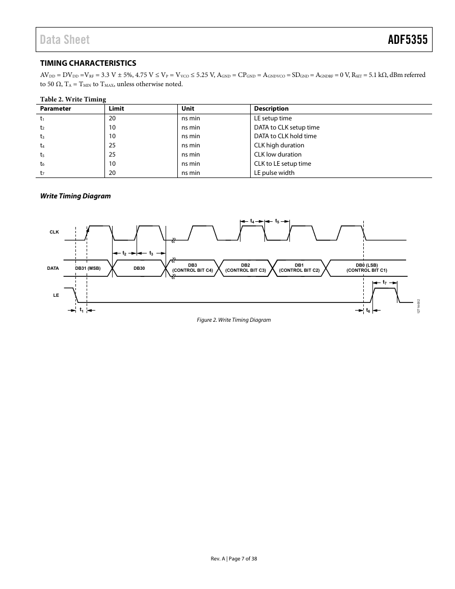
TIMING CHARACTERISTICS
AVDD = DVDD =VRF = 3.3 V ± 5%, 4.75 V ≤ VP = VVCO ≤ 5.25 V, AGND = CPGND = AGNDVCO = SDGND = AGNDRF = 0 V, RSET = 5.1 kΩ, dBm referred
to 50 Ω, TA = TMIN to TMAX, unless otherwise noted.
Unit
ns min
ns min
ns min
ns min
ns min
ns min
ns min
Table 2. Write Timing
Parameter
t1
t2
t3
t4
t5
t6
t7
Limit
20
10
10
25
25
10
20
Write Timing Diagram
CLK
t2
t3
Description
LE setup time
DATA to CLK setup time
DATA to CLK hold time
CLK high duration
CLK low duration
CLK to LE setup time
LE pulse width
t4
t5
DATA
DB31 (MSB)
DB30
DB3
(CONTROL BIT C4)
DB2
(CONTROL BIT C3)
DB1
(CONTROL BIT C2)
DB0 (LSB)
(CONTROL BIT C1)
LE
t1
Figure 2. Write Timing Diagram
t7
t6
2
0
0
-
4
1
7
2
1
Rev. A | Page 7 of 38
�
Data Sheet
Stresses at or above those listed under Absolute Maximum
Ratings may cause permanent damage to the product. This is a
stress rating only; functional operation of the product at these
or any other conditions above those indicated in the operational
section of this specification is not implied. Operation beyond
the maximum operating conditions for extended periods may
affect product reliability.
The ADF5355 is a high performance RF integrated circuit with
an ESD rating of 2.5 kV and is ESD sensitive. Take proper
precautions for handling and assembly.
TRANSISTOR COUNT
The transistor count for the ADF5355 is 103,665 (CMOS) and
3214 (bipolar).
ESD CAUTION
ADF5355
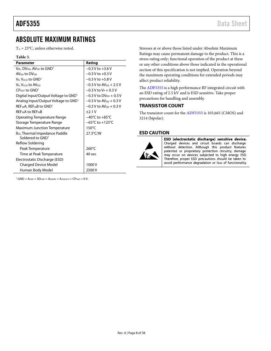
ABSOLUTE MAXIMUM RATINGS
TA = 25°C, unless otherwise noted.
Table 3.
Parameter
VRF, DVDD, AVDD to GND1
AVDD to DVDD
VP, VVCO to GND1
VP, VVCO to AVDD
CPOUT to GND1
Digital Input/Output Voltage to GND1
Analog Input/Output Voltage to GND1
REFINA, REFINB to GND1
REFINA to REFINB
Operating Temperature Range
Storage Temperature Range
Maximum Junction Temperature
θJA, Thermal Impedance Paddle
Soldered to GND1
Reflow Soldering
Peak Temperature
Time at Peak Temperature
Electrostatic Discharge (ESD)
Charged Device Model
Human Body Model
Rating
−0.3 V to +3.6 V
−0.3 V to +0.3 V
−0.3 V to +5.8 V
−0.3 V to AVDD + 2.5 V
−0.3 V to VP + 0.3 V
−0.3 V to DVDD + 0.3 V
−0.3 V to AVDD + 0.3 V
−0.3 V to AVDD + 0.3 V
±2.1 V
−40°C to +85°C
−65°C to +125°C
150°C
27.3°C/W
260°C
40 sec
1000 V
2500 V
1 GND = AGND = SDGND = AGNDRF = AGNDVCO = CPGND = 0 V.
Rev. A | Page 8 of 38
�



 2023年江西萍乡中考道德与法治真题及答案.doc
 2012年重庆南川中考生物真题及答案.doc
 2013年江西师范大学地理学综合及文艺理论基础考研真题.doc
 2020年四川甘孜小升初语文真题及答案I卷.doc
 2020年注册岩土工程师专业基础考试真题及答案.doc
 2023-2024学年福建省厦门市九年级上学期数学月考试题及答案.doc
 2021-2022学年辽宁省沈阳市大东区九年级上学期语文期末试题及答案.doc
 2022-2023学年北京东城区初三第一学期物理期末试卷及答案.doc
 2018上半年江西教师资格初中地理学科知识与教学能力真题及答案.doc
 2012年河北国家公务员申论考试真题及答案-省级.doc
 2020-2021学年江苏省扬州市江都区邵樊片九年级上学期数学第一次质量检测试题及答案.doc
 2022下半年黑龙江教师资格证中学综合素质真题及答案.doc