ET13X210/211
27MHz Receiver
ET13X210/211
27MHz Receiver
Etoms Electronics Corp.
Office:
6F, No. 12, Innovation 1st. RD.,
Science-Based Industrial Park,
Hsin-Chu City, Taiwan, R.O.C
Tel: +886-3-6661766 ext.1672
Fax: +886-3-6661765
This specification is subjected to be change without notice.
2003/02/18 V1
0
�
1. Descriptions
ET13X210/211
27MHz Receiver
The ET13X210/211 single-chip solution is an integrated circuit intended for use as a low cost
FSK receiver to establish a frequency-agile RF link. The device is designed to provide a
10-channel receiver. The chip is intended for digital (FSK) modulated applications in the
wireless Mouse and Keyboard. The single chip operates down to 2.7 V and is expressly
designed for low power consumption. The synthesizer has a typical channel spacing of
approximately 30KHz to allow narrow-band applications.
2. Feature
Include oscillation circuit with external X-TAL (4.0MHz).
n On-Chip Phase-Locked Loop (PLL)
n
n Standby mode for power saving.
n 2.7 to 5.5V supply range
3. Application
n Wireless Mouse
n Wireless Keyboard
n Wireless Communication Products
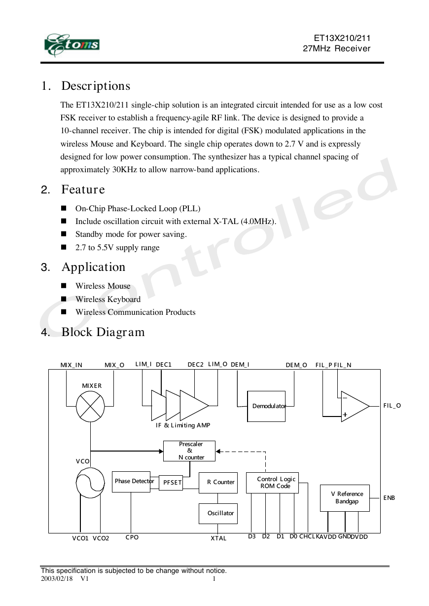
4. Block Diagram
MIX_IN
MIX_O
LIM_I
DEC1
DEC2
LIM_O
DEM_I
DEM_O
FIL_P
FIL_N
MIXER
V C O
IF & Limiting AMP
Prescaler
&
N counter
Demodulator
FIL_O
Phase Detector
PFSET
R Counter
Control Logic
ROM Code
Oscillator
V Reference
Bandgap
ENB
VCO1
VCO2
C P O
XTAL
D3 D2 D1 D0
CHCLK
AVDD
GND
DVDD
This specification is subjected to be change without notice.
2003/02/18 V1
1
�
5. PIN
n Pin Configuration
CHCLK
ENB
VCO1
VCO2
MIX_I
MIX_O
G N D
LIM_I
DEC1
DEC2
LIM_O
DEM_I
ET13X210/211
27MHz Receiver
D 3
ENB
VCO1
VCO2
MIX_I
MIX_O
G N D
LIM_I
DEC1
DEC2
LIM_O
DEM_I
V D D
X T A L
V D D
CPO
F I L _ P
G N D
FIL_O
FIL_N
DEM_O
D 2
D 1
D 0
V D D
X T A L
V D D
CPO
F I L _ P
G N D
FIL_O
FIL_N
DEM_O
SOP-24L (300mil)
DESCRIPTION
PIN
NAME
VDD
Positive power. A 0.1g F de-coupling capacitor should be
connected as close as possible from this pin to ground.
This pin should be a low inductance, direct connection to ground.
n Pin Descriptions
PIN NO
ET13X210 ET13X211
19, 21
19, 21
7,16
2
20
5
6
8
11
12
13
14
15
17
9
10
3
4
18
1
X
X
X
X
7,16
2
20
5
6
8
11
12
13
14
15
17
9
10
3
4
18
X
22
23
24
1
Inter Frequency Amplifier input.
GND
ENB Active Low, enable input.
XTAL Crystal (4MHz) Connection Input.
MIX_I RF signal input for mixer.
MIX_O Mixer signal output.
LIM_I
LIM_O Limiting amplifier output.
DEM_I Demodulator input.
DEM_O Demodulator output.
FIL_N Filter amplifier negative input.
FIL_O Filter amplifier output.
FIL_P Filter amplifier positive input.
DEC1
DEC2
VCO1 For external LC tank.
VCO2 For external LC tank.
CPO
CHCLK Clock input for channel selection.
D0
D1
D2
D3
The channel selected pin.
The channel selected pin.
The channel selected pin.
The channel selected pin.
This specification is subjected to be change without notice.
2003/02/18 V1
2
IF decoupling. External 0.1uFcapacitor connected to ground.
IF decoupling. External 0.1uFcapacitor connected to ground.
Phase detector output, connected to external low pass filter.
�
6. Function Description
ET13X210/211
27MHz Receiver
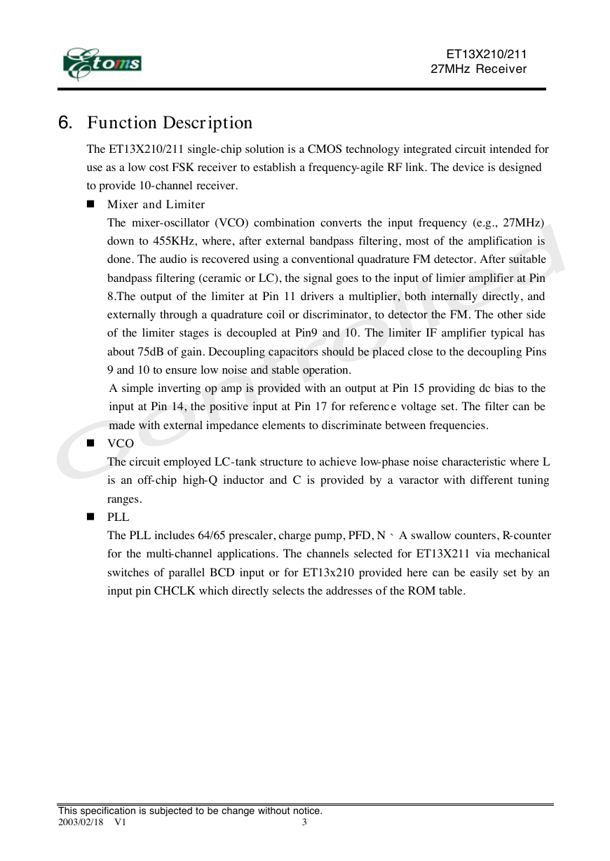
The ET13X210/211 single-chip solution is a CMOS technology integrated circuit intended for
use as a low cost FSK receiver to establish a frequency-agile RF link. The device is designed
to provide 10-channel receiver.
n Mixer and Limiter
The mixer-oscillator (VCO) combination converts the input frequency (e.g., 27MHz)
down to 455KHz, where, after external bandpass filtering, most of the amplification is
done. The audio is recovered using a conventional quadrature FM detector. After suitable
bandpass filtering (ceramic or LC), the signal goes to the input of limier amplifier at Pin
8.The output of the limiter at Pin 11 drivers a multiplier, both internally directly, and
externally through a quadrature coil or discriminator, to detector the FM. The other side
of the limiter stages is decoupled at Pin9 and 10. The limiter IF amplifier typical has
about 75dB of gain. Decoupling capacitors should be placed close to the decoupling Pins
9 and 10 to ensure low noise and stable operation.
A simple inverting op amp is provided with an output at Pin 15 providing dc bias to the
input at Pin 14, the positive input at Pin 17 for referenc e voltage set. The filter can be
made with external impedance elements to discriminate between frequencies.
n VCO
The circuit employed LC-tank structure to achieve low-phase noise characteristic where L
is an off-chip high-Q inductor and C is provided by a varactor with different tuning
ranges.
n PLL
The PLL includes 64/65 prescaler, charge pump, PFD, NB A swallow counters, R-counter
for the multi-channel applications. The channels selected for ET13X211 via mechanical
switches of parallel BCD input or for ET13x210 provided here can be easily set by an
input pin CHCLK which directly selects the addresses of the ROM table.
This specification is subjected to be change without notice.
2003/02/18 V1
3
�
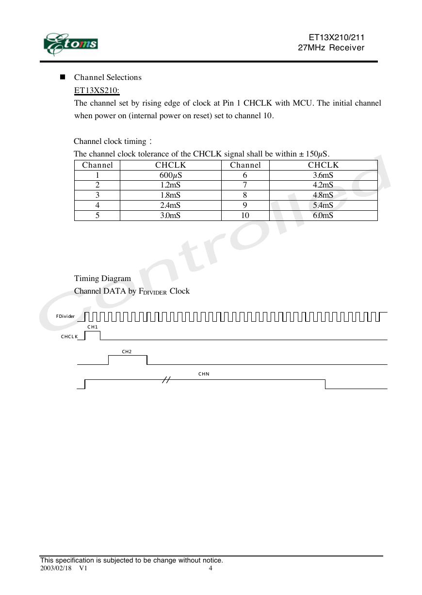
n Channel Selections
ET13X210/211
27MHz Receiver
ET13XS210:
The channel set by rising edge of clock at Pin 1 CHCLK with MCU. The initial channel
when power on (internal power on reset) set to channel 10.
Channel clock timingG
The channel clock tolerance of the CHCLK signal shall be within ± 150µS.
Channel
6
7
8
9
10
CHCLK
3.6mS
4.2mS
4.8mS
5.4mS
6.0mS
Channel
1
2
3
4
5
CHCLK
600µS
1.2mS
1.8mS
2.4mS
3.0mS
Timing Diagram
Channel DATA by FDIVIDER Clock
FDivider
C H C L K
C H 1
C H 2
C H N
This specification is subjected to be change without notice.
2003/02/18 V1
4
�
ET13X210/211
27MHz Receiver
ET13X211:
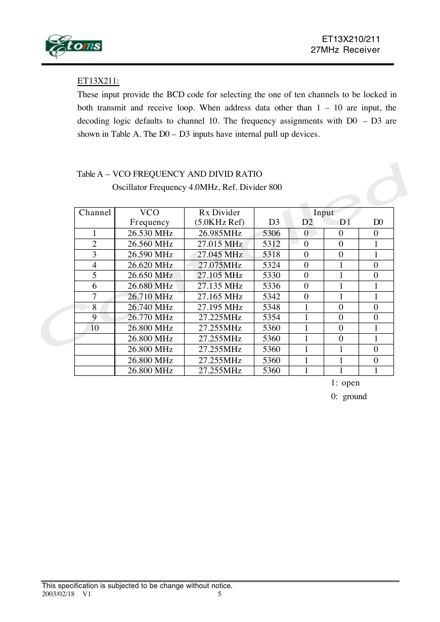
These input provide the BCD code for selecting the one of ten channels to be locked in
both transmit and receive loop. When address data other than 1 – 10 are input, the
decoding logic defaults to channel 10. The frequency assignments with D0 – D3 are
shown in Table A. The D0 – D3 inputs have internal pull up devices.
Table A – VCO FREQUENCY AND DIVID RATIO
Oscillator Frequency 4.0MHz, Ref. Divider 800
Input
VCO
Channel
Frequency
26.530 MHz
26.560 MHz
26.590 MHz
26.620 MHz
26.650 MHz
26.680 MHz
26.710 MHz
26.740 MHz
26.770 MHz
26.800 MHz
26.800 MHz
26.800 MHz
26.800 MHz
26.800 MHz
Rx Divider
(5.0KHz Ref)
26.985MHz
27.015 MHz
27.045 MHz
27.075MHz
27.105 MHz
27.135 MHz
27.165 MHz
27.195 MHz
27.225MHz
27.255MHz
27.255MHz
27.255MHz
27.255MHz
27.255MHz
D3 D2 D1 D0
0
1
1
0
0
1
1
0
0
1
1
0
0
1
5306
5312
5318
5324
5330
5336
5342
5348
5354
5360
5360
5360
5360
5360
0
0
0
0
0
0
0
1
1
1
1
1
1
1
0
0
0
1
1
1
1
0
0
0
0
1
1
1
1
2
3
4
5
6
7
8
9
10
1: open
0: ground
This specification is subjected to be change without notice.
2003/02/18 V1
5
�
ET13X210/211
27MHz Receiver
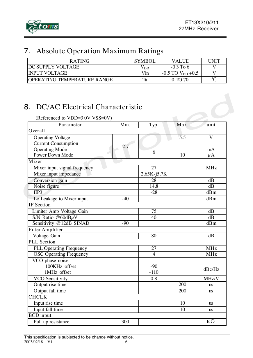
7. Absolute Operation Maximum Ratings
RATING
DC SUPPLY VOLTAGE
INPUT VOLTAGE
OPERATING TEMPERATURE RANGE
SYMBOL
VDD
Vin
Ta
VALUE
-0.3 To 6
-0.5 TO VDD +0.5
0 TO 70
UNIT
V
V
J
8. DC/AC Electrical Characteristic
(Referenced to VDD=3.0V VSS=0V)
Parameter
Min.
Typ.
Max.
Overall
Operating Voltage
Current Consumption
Operating Mode
Power Down Mode
Mixer
Mixer input signal frequency
Mixer input impedance
Conversion gain
Noise figure
IIP3
Lo Leakage to Mixer input
IF Section
Limiter Amp Voltage Gain
S/N Ratio @60dBµV
Sensitivity @12dB SINAD
Filter Amplifier
Voltage Gain
PLL Section
PLL Operating Frequency
OSC Operating Frequency
VCO phase noise
100KHz offset
1MHz offset
VCO Sensitivity
Output rise time
Output fall time
CHCLK
Input rise time
Input fall time
BCD input
Pull up resistance
2.7
-40
-90
300
6
27
2.65K-j5.7K
28
14.8
-28
75
40
80
27
4
-90
-110
0.8
5.5
10
200
200
10
10
This specification is subjected to be change without notice.
2003/02/18 V1
6
unit
V
mA
µA
MHz
dB
dB
dBm
dBm
dB
dB
dBm
dB
MHz
MHz
dBc/Hz
MHz/V
ns
ns
us
us
K[
�
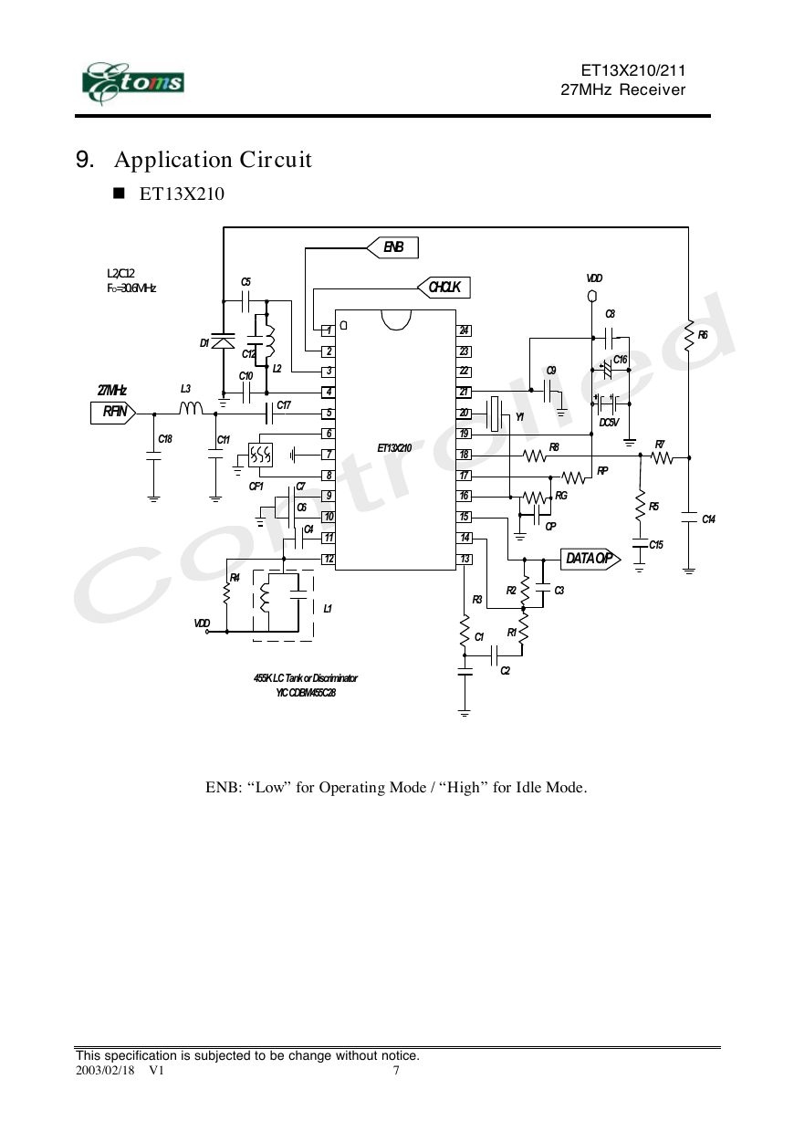
9. Application Circuit
n ET13X210
L2/C12
FO=30.6MHz
27MHz
RFIN
D1
L3
C18
C11
C5
C12
C10
L2
C17
CF1
C7
C6
C4
R4
VDD
1
2
3
4
5
6
7
8
9
10
11
12
L1
455K LC Tank or Discriminator
YIC CDBM455C28
ET13X210/211
27MHz Receiver
ENB
CHCLK
ET13X210
24
23
22
21
20
19
18
17
16
15
14
13
VDD
C8
C16
DC5V
RP
Y1
C9
R8
RG
CP
DATA O/P
C3
R3
C1
R2
R1
C2
R6
C14
R7
R5
C15
ENB: “Low” for Operating Mode / “High” for Idle Mode.
This specification is subjected to be change without notice.
2003/02/18 V1
7
�




 2023年江西萍乡中考道德与法治真题及答案.doc
 2012年重庆南川中考生物真题及答案.doc
 2013年江西师范大学地理学综合及文艺理论基础考研真题.doc
 2020年四川甘孜小升初语文真题及答案I卷.doc
 2020年注册岩土工程师专业基础考试真题及答案.doc
 2023-2024学年福建省厦门市九年级上学期数学月考试题及答案.doc
 2021-2022学年辽宁省沈阳市大东区九年级上学期语文期末试题及答案.doc
 2022-2023学年北京东城区初三第一学期物理期末试卷及答案.doc
 2018上半年江西教师资格初中地理学科知识与教学能力真题及答案.doc
 2012年河北国家公务员申论考试真题及答案-省级.doc
 2020-2021学年江苏省扬州市江都区邵樊片九年级上学期数学第一次质量检测试题及答案.doc
 2022下半年黑龙江教师资格证中学综合素质真题及答案.doc