logo资料库

intel 千兆网卡开发手册.pdf

第1页 / 共522页
第2页 / 共522页
第3页 / 共522页
第4页 / 共522页
第5页 / 共522页
第6页 / 共522页
第7页 / 共522页
第8页 / 共522页
资料共522页,剩余部分请下载后查看
Introduction 1
1.1 Scope
1.2 Overview
1.3 Ethernet Controller Features
1.3.1 PCI Features
1.3.2 Network Side Features
1.3.3 Host Offloading Features
1.3.4 Additional Performance Features
1.3.5 Manageability Features
1.3.6 Additional Ethernet Controller Features
1.3.7 Technology Features
1.4 Conventions
1.4.1 Register and Bit References
1.4.2 Byte and Bit Designations
1.5 Related Documents
1.6 Memory Alignment Terminology
Architectural Overview 2
2.1 Introduction
2.2 External Architecture
2.3 Microarchitecture
2.3.1 Integrated 10/100/1000 Mb/s PHY
2.3.2 System Interface
2.3.3 EEPROM Interface
2.3.4 Flash Memory Interface
2.4 DMA Addressing
2.5 Ethernet Addressing
2.6 Interrupt Control and Tuning
2.7 Hardware Acceleration Capability
2.7.1 Jumbo Frame Support
2.7.2 Receive and Transmit Checksum Offloading
2.7.3 TCP Segmentation
2.7.4 Receive Fragmented UDP Checksum Offloading
2.8 Buffer and Descriptor Structure
2.9 Multiple Transmit Queues
2.9.1 Quality of Service (QoS)
2.9.2 Resource Locking Prevention
2.10 iSCSI HBA Support During Boot (82571/82572/ 631xESB/632xESB)
Receive and Transmit Description 3
3.1 Introduction
3.2 Packet Reception
3.2.1 Packet Address Filtering
3.2.2 Receive Data Storage
3.2.3 Receive Descriptor Queue Structure
3.2.4 Receive Descriptor Format
3.2.5 Extended Rx Descriptor
3.2.6 Receive UDP Fragmentation Checksum
3.2.7 Packet Split Receive Descriptor
3.2.8 Using Extended Rx Descriptors
3.2.9 Receive Descriptor Fetching
3.2.10 Receive Descriptor Write-Back
3.2.11 Receive Interrupts
3.2.12 Receive Packet Checksum Offloading
3.2.13 Manageability Receive Filtering
3.2.14 Multiple Receive Queues & Receive-Side Scaling (RSS)
3.2.15 RSS Verification Suite
3.3 Transmit Descriptor Ring Structure
3.3.1 Transmit Descriptor Fetching
3.3.2 Transmit Descriptor Write-Back
3.3.3 Transmit Interrupts
3.4 Packet Transmission
3.4.1 Transmit Data Storage
3.4.2 Transmit Descriptors
3.4.3 Legacy Transmit Descriptor Format
3.4.4 Transmit Descriptor Special Field Format
3.4.5 TCP/IP Context Transmit Descriptor Format
3.4.6 TCP/IP Context Descriptor Layout
3.4.7 TCP/IP Data Descriptor Format
3.5 IP and TCP Transmit Checksum Offloading
3.5.1 Pipelined Tx Data Read Requests
3.6 TCP Segmentation
3.6.1 Assumptions
3.6.2 Transmission Process
3.6.3 TCP Segmentation Performance
3.6.4 Packet Format
3.6.5 TCP Segmentation Context Descriptor
3.6.6 TCP Segmentation Data Descriptors
3.6.7 TCP Segmentation Source Data
3.6.8 TCP Segmentation Use of Multiple Data Descriptors
3.6.9 IP and TCP Headers
3.6.10 Transmit Checksum Offloading with TCP Segmentation
3.6.11 IP and TCP Header Updating
3.6.12 Limitations and Software Considerations
PCIe* Local Bus Interface 4
4.1 Introduction
4.2 General Functionality
4.2.1 Message Handling (Receive Side)
4.2.2 Message Handling (Transmit Side)
4.2.3 Data Alignment
4.2.4 Transaction Attributes
4.2.5 Error Forwarding
4.3 Flow Control
4.3.1 Flow Control Rules
4.3.2 Upstream Flow Control Tracking
4.3.3 Flow Control Update Frequency
4.3.4 Flow Control Timeout Mechanism
4.4 Host Interface
4.4.1 Tag IDs
4.4.2 Completion Timeout Mechanism
4.5 Error Events and Error Reporting
4.5.1 Error Events
4.5.2 Error Pollution
4.5.3 Unsuccessful Completion Status
4.6 Link Layer
4.6.1 ACK/NAK Scheme
4.6.2 Supported DLLPs
4.6.3 Transmit EDB Nullifying
4.7 Physical Layer
4.7.1 Link Width
4.7.2 Polarity Inversion (82571EB/82572EI)
4.7.3 Lane-To-Lane De-Skew (82571EB/82572EI)
4.7.4 Lane Reversal (82571EB/82572EI)
4.7.5 Performance Monitoring
4.7.6 Configuration Registers
4.7.7 Mandatory PCI Configuration Registers
4.7.8 UHCI Registers (631xESB/632xESB only)
4.7.9 PCI Power Management Registers
EEPROM/NVM Interface 5
5.1 Introduction
5.2 EEPROM Device (82571EB/82572EI/631xESB/ 632xESB)
5.2.1 Software Accesses
5.2.2 Signature and CRC Fields
5.2.3 Protected EEPROM Space (82571EB/82572EI)
5.2.4 Protected EEPROM Space (631xESB/632xESB)
5.2.5 Initial EEPROM Programming
5.2.6 Activating the Protection Mechanism
5.2.7 Initial EEPROM Programming
5.3 EEPROM Firmware/Software Synchronization (631xESB/ 632xESB)
5.4 EEPROM/PHY Firmware/Software Synchronization (82571EB)
5.5 NVM Device (82573E/82573V/82573L)
5.5.1 Supported NVM Devices
5.5.2 NVM Device Detection
5.5.3 Device Operation with EEPROM
5.5.4 Device Operation with Flash
5.5.5 EEPROM Mode
5.5.6 NVM Clients
5.6 EEPROM/NVM Map
5.6.1 Hardware Accessed Words
5.6.2 Flash Software Detection Word 23h (82573E/82573V/82573L)
5.6.3 CRID3 Word 27h, High (631xESB/632xESB)
5.6.4 CRID2 Word 27h, Low (631xESB/632xESB)
5.6.5 Intel® AMT MAC Address Words 80h - 82h (82573E)
5.6.6 Vital Product Data Pointer (Word 2Fh)
5.6.7 ASF Controller Words
5.7 Software Owned EEPROM Words Description
5.7.1 EEPROM Map for Words 03h:09h and 30h:3Fh
5.7.2 Software Compatibility Word 1 (Word 03h)
5.7.3 OEM LED Configuration Word (Word 04h)
5.7.4 EEPROM Image Version Word (Word 05h)
5.7.5 631xESB/632xESB SerDes Adjustment (Word 06h)
5.7.6 631xESB/632xESB Software Configuration (Word 07h)
5.7.7 OEM Configuration (Words 06h:07h)
5.7.8 PBA Number or OEM Version (Words 08h, 09h)
5.7.9 PXE Code (Words 30h – 35h)
5.7.10 Alternate MAC Address (Word 37h)
5.7.11 iSCSI Boot Configuration Pointer (Word 3Dh)
5.7.12 iSCSI Module Structure1
5.7.13 Checksum Word Calculation (Word 3Fh)
Power Management 6
6.1 Introduction
6.1.1 Assumptions
6.1.2 Power Targets
6.1.3 Introduction to Power States
6.1.4 Auxiliary Power Usage
6.1.5 Auxiliary Power Usage (631xESB/632xESB)
6.1.6 Form Factor Power Limits
6.1.7 Unit Power Reduction Measures
6.1.8 Power States
6.1.9 Power-State Transitions Timing
6.2 Wake-Up
6.2.1 Advanced Power Management Wakeup
6.2.2 PCIe Power Management Wakeup
6.2.3 Wake-Up Packets
FLASH Memory Interface 7
7.1 Introduction
7.1.1 Flash Interface Operation
7.1.2 Flash Write Control
7.1.3 Flash Erase Control
Ethernet Interface 8
8.1 Introduction
8.1.1 82571EB/82572EI GMII/MII Interface
8.1.2 82573E/82573V/82573L GMII/MII Interface
8.1.3 Internal MAC/PHY GMII/MII Interface
8.1.4 MDIO/MDC1
8.2 Duplex Operation for Copper
8.2.1 Full Duplex
8.2.2 Half Duplex
8.2.3 Gigabit Physical Coding Sub-Layer (PCS) for TBI/SerDes
8.3 Auto-Negotiation and Link Setup
8.3.1 Fiber/TBI Link Configuration
8.3.2 Link Configuration in 10/100/1000Base-T Mode
8.3.3 Loss of Signal/Link Status Indication
8.4 10/100 Mb/s Specific Performance Enhancements
8.4.1 Adaptive IFS
8.4.2 Flow Control
8.4.3 MAC Control Frames & Reception of Flow Control Packets
8.4.4 Discard PAUSE Frames and Pass MAC Control Frames
8.4.5 Transmission of PAUSE Frames
8.4.6 Software Initiated PAUSE Frame Transmission
8.5 GLCI Interface (631xESB/632xESB and 82563EB/ 82564EB Only)
8.5.1 GLCI Operation
8.5.2 Inband Messages
8.6 Ethernet Port
8.7 GLCI In-Band Access
802.1q VLAN Support 9
9.1 802.1q VLAN Packet Format
9.1.1 802.1q Tagged Frames
9.2 Transmitting and Receiving 802.1q Packets
9.2.1 Adding 802.1q Tags on Transmits
9.2.2 Stripping 802.1q Tags on Receives
9.3 802.1q VLAN Packet Filtering
Configurable LED Outputs 10
10.1 Configurable LED Outputs
PHY Functionality and Features 11
11.1 Auto-Negotiation
11.1.1 Overview
11.1.2 Next Page Exchanges
11.1.3 Register Update
11.1.4 Status
11.2 MDI/MDI-X Crossover
11.2.1 Polarity Correction
11.2.2 10/100 Downshift
11.3 Cable Length Detection
11.4 PHY Power Management
11.4.1 Link Down – Energy Detect
11.4.2 D3 State, No Link Required
11.4.3 D3 Link-Up, Speed-Management Enabled
11.4.4 D3 Link-Up, Speed-Management Disabled
11.5 Initialization
11.5.1 MDIO Control Mode
11.6 Determining Link State
11.6.1 False Link
11.6.2 Forced Operation
11.6.3 Auto Negotiation
11.6.4 Parallel Detection
11.7 Link Criteria
11.7.1 1000BASE-T
11.7.2 100BASE-TX
11.7.3 10BASE-T
11.8 Link Enhancements
11.8.1 SmartSpeed
11.8.2 Flow Control
11.9 Management Data Interface
11.10 Low Power Operation
11.10.1 Powerdown via the PHY Register
11.10.2 Smart Power-Down
11.11 1000 Mb/s Operation
11.11.1 Introduction
11.11.2 Transmit Functions
11.12 100 Mb/s Operation
11.13 10 Mb/s Operation
11.13.1 Link Test
11.13.2 10Base-T Link Failure Criteria and Override1
11.13.3 Jabber
11.13.4 Polarity Correction
11.13.5 Dribble Bits
11.14 PHY Line Length Indication
Dual Port Characteristics 12
12.1 Introduction
12.2 Features of Each MAC
12.2.1 PCIe* Interface
12.2.2 MAC Configuration Register Space
12.2.3 SDP, LED, INT# output
12.3 Shared EEPROM
12.3.1 EEPROM Map
12.4 Shared FLASH
12.4.1 FLASH Access Contention
12.5 Link Mode/Configuration
12.6 LAN Disable
12.6.1 Overview
12.6.2 Values Sampled on Reset
12.6.3 Multi-Function Advertisement
12.6.4 Interrupt Use
12.6.5 Power Reporting
Register Descriptions 13
13.1 Introduction
13.2 Register Conventions
13.2.1 Memory and I/O Address Decoding
13.2.2 I/O-Mapped Internal Register, Internal Memory, and Flash
13.3 Main Register Descriptions
13.3.1 Device Control Register
13.3.2 Device Status Register
13.3.3 EEPROM/Flash Control Register
13.3.4 EEPROM Read Register
13.3.5 Extended Device Control Register
13.3.6 Flash Access
13.3.7 MDI Control Register
13.3.8 PHY Registers
13.3.9 PHY Address and Page Register (82563EB/82564EB)
13.3.10 SERDES ANA (82571EB/82572EI)
13.3.11 Flow Control Address Low
13.3.12 Flow Control Address High
13.3.13 Flow Control Type
13.3.14 GLCI Control and Status Registers (631xESB/632xESB)
13.3.15 VLAN Ether Type
13.3.16 MDC/MDIO PHY Address Register (631xESB/632xESB)
13.3.17 ULT Fuse Register 3 (82573E/82573V/82573L)
13.3.18 Flow Control Transmit Timer Value
13.3.19 Transmit Configuration Word Register
13.3.20 Receive Configuration Word Register
13.3.21 LED Control
13.3.22 Extended Configuration Control (82573E/82573V/82573L)
13.3.23 Extended Configuration Size (82573E/82573V/82573L)
13.3.24 Packet Buffer Allocation
13.3.25 MNG EEPROM Control Register (82571EB and 82573E/82573V/ 82573L)
13.3.26 Software/Firmware Synchronization (631xESB/632xESB)
13.3.27 Interrupt Cause Read Register
13.3.28 Interrupt Throttling Rate
13.3.29 Interrupt Cause Set Register
13.3.30 Interrupt Mask Set/Read Register
13.3.31 Interrupt Mask Clear Register
13.3.32 Interrupt Acknowledge Auto Mask Register
13.3.33 Receive Control Register
13.3.34 Early Receive Threshold (82573E/82573V/82573L)
13.3.35 Flow Control Receive Threshold Low
13.3.36 Flow Control Receive Threshold High
13.3.37 Packet Split Receive Control Register
13.3.38 Receive Descriptor Base Address Low Queue 0
13.3.39 Receive Descriptor Base Address High Queue 0
13.3.40 Receive Descriptor Length Queue 0
13.3.41 Receive Descriptor Head Queue 0
13.3.42 Receive Descriptor Tail Queue 0
13.3.43 Receive Interrupt Delay Timer (Packet Timer) Register
13.3.44 Receive Descriptor Control
13.3.45 Receive Interrupt Absolute Delay Timer
13.3.46 Receive Descriptor Base Address Low Queue 1
13.3.47 Receive Descriptor Base Address High Queue 1
13.3.48 Receive Descriptor Length Queue 1
13.3.49 Receive Descriptor Head Queue 1
13.3.50 Receive Descriptor Tail Queue 1
13.3.51 Receive Descriptor Control 1
13.3.52 Receive Small Packet Detect Interrupt
13.3.53 Receive ACK Interrupt Delay Register
13.3.54 CPU Vector Register
13.3.55 Receive Checksum Control
13.3.56 Receive Filter Control Register
13.3.57 Transmit Control Register
13.3.58 Transmit Control Extended (631xESB/632xESB)
13.3.59 Transmit IPG Register
13.3.60 Adaptive IFS Throttle Register
13.3.61 Transmit Descriptor Base Address Low
13.3.62 Transmit Descriptor Base Address High
13.3.63 Transmit Descriptor Length
13.3.64 Transmit Descriptor Head
13.3.65 Transmit Descriptor Tail
13.3.66 Transmit Interrupt Delay Value
13.3.67 Transmit Descriptor Control
13.3.68 Transmit Absolute Interrupt Delay Value
13.3.69 Transmit Arbitration Counter Queue 0
13.3.70 Transmit Descriptor Base Address Low Queue 1
13.3.71 Transmit Descriptor Base Address High Queue 1
13.3.72 Transmit Descriptor Length Queue 1
13.3.73 Transmit Descriptor Head Queue 1
13.3.74 Transmit Descriptor Tail Queue 1
13.3.75 Transmit Descriptor Control 1
13.3.76 Transmit Arbitration Counter Queue 1
13.4 Filter Registers
13.4.1 Multicast Table Array
13.4.2 Receive Address Low
13.4.3 Receive Address High
13.4.4 VLAN Filter Table Array
13.4.5 Multiple Receive Queues Command Register
13.4.6 RSS Interrupt Mask Register
13.4.7 RSS Interrupt Request Register
13.4.8 Redirection Table
13.4.9 RSS Random Key Register
13.5 Wakeup Registers
13.5.1 Wakeup Control Register
13.5.2 Wakeup Filter Control Register
13.5.3 Wakeup Status Register
13.5.4 IP Address Valid
13.5.5 IPv4 Address Table
13.5.6 IPv6 Address Table
13.5.7 Wakeup Packet Length
13.5.8 Wakeup Packet Memory (128 Bytes)
13.5.9 Flexible Filter Length Table
13.5.10 Flexible Filter Mask Table
13.5.11 Flexible Filter Value Table
13.6 MNG Register (82571EB)
13.6.1 Management Control Register
13.7 Packet Buffer ECC Register (82571EB)
13.8 PCIe* Registers
13.8.1 PCIe* Control
13.8.2 PCIe* Statistics Control #1
13.8.3 PCIe* Statistics Control #2
13.8.4 PCIe* Statistics Control #3
13.8.5 PCIe* Statistics Control #4
13.8.6 PCIe* Counter #0
13.8.7 PCIe* Counter #1
13.8.8 PCIe* Counter #2
13.8.9 PCIe* Counter #3
13.8.10 Function Active and Power State to MNG
13.8.11 SerDes/CCM/PCIe* CSR (82571EB/82572EI)
13.8.12 SerDes/CCM/PCIe* CSR (82571EB/82572EI)
13.8.13 SerDes/CCM/PCIe* CSR (82571EB/82572EI)
13.8.14 SerDes/CCM/PCIe* CSR (82571EB/82572EI)
13.8.15 Analog Control Register (631xESB/632xESB)
13.8.16 SerDes/CCM/PCIe* CSR (82571EB/82572EI)
13.8.17 Software Semaphore Register
13.8.18 Firmware Semaphore Register
13.9 Statistics Registers
13.9.1 CRC Error Count
13.9.2 Alignment Error Count
13.9.3 Symbol Error Count
13.9.4 RX Error Count
13.9.5 Missed Packets Count
13.9.6 Single Collision Count
13.9.7 Excessive Collisions Count
13.9.8 Multiple Collision Count
13.9.9 Late Collisions Count
13.9.10 Collision Count
13.9.11 Defer Count
13.9.12 Transmit with No CRS
13.9.13 Sequence Error Count
13.9.14 Carrier Extension Error Count (631xESB/632xESB)
13.9.15 Receive Length Error Count
13.9.16 XON Received Count
13.9.17 XON Transmitted Count
13.9.18 XOFF Received Count
13.9.19 XOFF Transmitted Count
13.9.20 FC Received Unsupported Count
13.9.21 Packets Received (64 Bytes) Count
13.9.22 Packets Received (65-127 Bytes) Count
13.9.23 Packets Received (128-255 Bytes) Count
13.9.24 Packets Received (256-511 Bytes) Count
13.9.25 Packets Received (512-1023 Bytes) Count
13.9.26 Packets Received (1024 to Max Bytes) Count
13.9.27 Good Packets Received Count
13.9.28 Broadcast Packets Received Count
13.9.29 Multicast Packets Received Count
13.9.30 Good Packets Transmitted Count
13.9.31 Good Octets Received Count
13.9.32 Good Octets Transmitted Count
13.9.33 Receive No Buffers Count
13.9.34 Receive Undersize Count
13.9.35 Receive Fragment Count
13.9.36 Receive Oversize Count
13.9.37 Receive Jabber Count
13.9.38 Management Packets Received Count
13.9.39 Management Packets Dropped Count
13.9.40 Management Packets Transmitted Count
13.9.41 Total Octets Received
13.9.42 Total Octets Transmitted
13.9.43 Total Packets Received
13.9.44 Total Packets Transmitted
13.9.45 Packets Transmitted (64 Bytes) Count
13.9.46 Packets Transmitted (65-127 Bytes) Count
13.9.47 Packets Transmitted (128-255 Bytes) Count
13.9.48 Packets Transmitted (256-511 Bytes) Count
13.9.49 Packets Transmitted (512-1023 Bytes) Count
13.9.50 Packets Transmitted (1024 Bytes or Greater) Count
13.9.51 Multicast Packets Transmitted Count
13.9.52 Broadcast Packets Transmitted Count
13.9.53 TCP Segmentation Context Transmitted Count
13.9.54 TCP Segmentation Context Tx Fail Count
13.9.55 Interrupt Assertion Count
13.9.56 Interrupt Cause Rx Packet Timer Expire Count
13.9.57 Interrupt Cause Rx Absolute Timer Expire Count
13.9.58 Interrupt Cause Tx Packet Timer Expire Count
13.9.59 Interrupt Cause Tx Absolute Timer Expire Count
13.9.60 Interrupt Cause Transmit Queue Empty Count
13.9.61 Interrupt Cause Transmit Descriptor Low Threshold Count
13.9.62 Interrupt Cause Receive Descriptor Minimum Threshold Count
13.9.63 Interrupt Cause Receive Overrun Count
General Initialization and Reset Operation 14
14.1 Introduction
14.2 Power Up State
14.3 Initialization Sequence
14.4 Interrupts During Initialization
14.5 Global Reset and General Configuration
14.6 Receive Initialization
14.6.1 Initialize the Receive Control Register
14.7 Transmit Initialization
14.8 Link Setup Mechanisms and Control/Status Bit Summary
14.8.1 PHY Initialization
14.8.2 MAC/PHY Link Setup
14.8.3 MAC/SerDes (TBI-Mode) Link Setup
14.9 Reset Operation
14.10 Initialization of Statistics
Diagnostics and Testability 15
15.1 Diagnostics
15.1.1 FIFO Pointer Accessibility
15.1.2 FIFO Data Accessibility
15.1.3 Loopback Operations
15.2 Testability
15.2.1 EXTEST Instruction
15.2.2 SAMPLE/PRELOAD Instruction
15.2.3 IDCODE Instruction
15.2.4 BYPASS Instruction
PCIe* GbE Controllers Open Source Software Developer’s Manual 631xESB/632xESB, 82563EB/82564EB, 82571EB/82572EI & 82573E/ 82573V/82573L 316080-014 Revision 2.4
PCIe* GbE Controllers Open Source Software Developer’s Manual Legal Notice INFORMATION IN THIS DOCUMENT IS PROVIDED IN CONNECTION WITH INTEL PRODUCTS. NO LICENSE, EXPRESS OR IMPLIED, BY ESTOPPEL OR OTHERWISE, TO ANY INTELLECTUAL PROPERTY RIGHTS IS GRANTED BY THIS DOCUMENT. EXCEPT AS PROVIDED IN INTEL'S TERMS AND CONDITIONS OF SALE FOR SUCH PRODUCTS, INTEL ASSUMES NO LIABILITY WHATSOEVER AND INTEL DISCLAIMS ANY EXPRESS OR IMPLIED WARRANTY, RELATING TO SALE AND/OR USE OF INTEL PRODUCTS INCLUDING LIABILITY OR WARRANTIES RELATING TO FITNESS FOR A PARTICULAR PURPOSE, MERCHANTABILITY, OR INFRINGEMENT OF ANY PATENT, COPYRIGHT OR OTHER INTELLECTUAL PROPERTY RIGHT. UNLESS OTHERWISE AGREED IN WRITING BY INTEL, THE INTEL PRODUCTS ARE NOT DESIGNED NOR INTENDED FOR ANY APPLICATION IN WHICH THE FAILURE OF THE INTEL PRODUCT COULD CREATE A SITUATION WHERE PERSONAL INJURY OR DEATH MAY OCCUR. Intel may make changes to specifications and product descriptions at any time, without notice. Designers must not rely on the absence or characteristics of any features or instructions marked "reserved" or "undefined." Intel reserves these for future definition and shall have no responsibility whatsoever for conflicts or incompatibilities arising from future changes to them. The information here is subject to change without notice. Do not finalize a design with this information. The products described in this document may contain design defects or errors known as errata which may cause the product to deviate from published specifications. Current characterized errata are available on request. Contact your local Intel sales office or your distributor to obtain the latest specifications and before placing your product order. Copies of documents which have an order number and are referenced in this document, or other Intel literature, may be obtained by calling 1-800-548-4725, or go to: http://www.intel.com/design/literature.htm. Intel® is a trademark or registered trademark of Intel Corporation or its subsidiaries in the United States and other countries. * Other names and brands may be claimed as the property of others. Copyright © Intel Corporation, 2011 ii
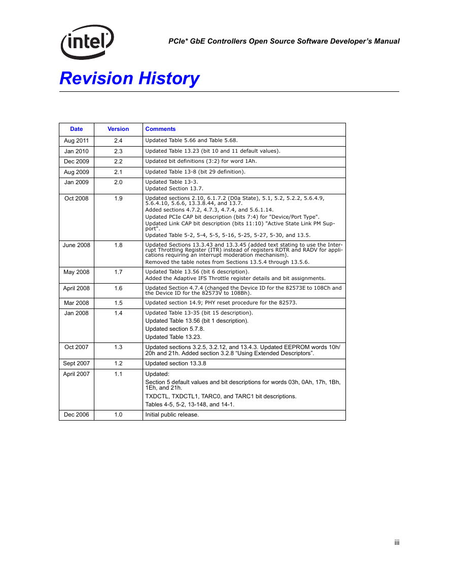
PCIe* GbE Controllers Open Source Software Developer’s Manual Revision History Date Aug 2011 Jan 2010 Dec 2009 Aug 2009 Jan 2009 Oct 2008 June 2008 May 2008 April 2008 Mar 2008 Jan 2008 Oct 2007 Sept 2007 April 2007 2.4 2.3 2.2 2.1 2.0 1.9 1.8 1.7 1.6 1.5 1.4 1.3 1.2 1.1 Dec 2006 1.0 Version Comments Updated Table 5.66 and Table 5.68. Updated Table 13.23 (bit 10 and 11 default values). Updated bit definitions (3:2) for word 1Ah. Updated Table 13-8 (bit 29 definition). Updated Table 13-3. Updated Section 13.7. Updated sections 2.10, 6.1.7.2 (D0a State), 5.1, 5.2, 5.2.2, 5.6.4.9, 5.6.4.10, 5.6.6, 13.3.8.44, and 13.7. Added sections 4.7.2, 4.7.3, 4.7.4, and 5.6.1.14. Updated PCIe CAP bit description (bits 7:4) for "Device/Port Type". Updated Link CAP bit description (bits 11:10) "Active State Link PM Sup- port". Updated Table 5-2, 5-4, 5-5, 5-16, 5-25, 5-27, 5-30, and 13.5. Updated Sections 13.3.43 and 13.3.45 (added text stating to use the Inter- rupt Throttling Register (ITR) instead of registers RDTR and RADV for appli- cations requiring an interrupt moderation mechanism). Removed the table notes from Sections 13.5.4 through 13.5.6. Updated Table 13.56 (bit 6 description). Added the Adaptive IFS Throttle register details and bit assignments. Updated Section 4.7.4 (changed the Device ID for the 82573E to 108Ch and the Device ID for the 82573V to 108Bh). Updated section 14.9; PHY reset procedure for the 82573. Updated Table 13-35 (bit 15 description). Updated Table 13.56 (bit 1 description). Updated section 5.7.8. Updated Table 13.23. Updated sections 3.2.5, 3.2.12, and 13.4.3. Updated EEPROM words 10h/ 20h and 21h. Added section 3.2.8 “Using Extended Descriptors”. Updated section 13.3.8 Updated: Section 5 default values and bit descriptions for words 03h, 0Ah, 17h, 1Bh, 1Eh, and 21h. TXDCTL, TXDCTL1, TARC0, and TARC1 bit descriptions. Tables 4-5, 5-2, 13-148, and 14-1. Initial public release. iii
PCIe* GbE Controllers Open Source Software Developer’s Manual Note: This page intentionally left blank. iv
Contents Contents 1 1.1 1.2 1.3 Introduction ..................................................................................................................1 Scope............................................................................................................................................1 Overview.......................................................................................................................................1 Ethernet Controller Features ........................................................................................................1 PCI Features................................................................................................................1 1.3.1 Network Side Features ................................................................................................2 1.3.2 Host Offloading Features.............................................................................................2 1.3.3 1.3.4 Additional Performance Features ................................................................................3 Manageability Features ...............................................................................................3 1.3.5 Additional Ethernet Controller Features.......................................................................4 1.3.6 1.3.7 Technology Features ...................................................................................................4 Conventions..................................................................................................................................5 Register and Bit References........................................................................................5 1.4.1 1.4.2 Byte and Bit Designations............................................................................................5 Related Documents ......................................................................................................................5 Memory Alignment Terminology ...................................................................................................5 Architectural Overview ............................................................................................7 Introduction...................................................................................................................................7 External Architecture ....................................................................................................................8 Microarchitecture ........................................................................................................................11 Integrated 10/100/1000 Mb/s PHY ............................................................................11 2.3.1 System Interface........................................................................................................12 2.3.2 2.3.3 EEPROM Interface ....................................................................................................12 2.3.4 Flash Memory Interface .............................................................................................12 DMA Addressing.........................................................................................................................12 Ethernet Addressing ...................................................................................................................13 Interrupt Control and Tuning.......................................................................................................14 Hardware Acceleration Capability...............................................................................................15 Jumbo Frame Support ...............................................................................................15 2.7.1 Receive and Transmit Checksum Offloading ............................................................16 2.7.2 2.7.3 TCP Segmentation ....................................................................................................16 2.7.4 Receive Fragmented UDP Checksum Offloading .....................................................16 Buffer and Descriptor Structure ..................................................................................................16 Multiple Transmit Queues...........................................................................................................17 Quality of Service (QoS) ............................................................................................17 2.9.1 2.9.2 Resource Locking Prevention....................................................................................17 iSCSI HBA Support During Boot (82571/82572/631xESB/632xESB) ........................................17 1.4 1.5 1.6 2 2.1 2.2 2.3 2.4 2.5 2.6 2.7 2.8 2.9 2.10 iii
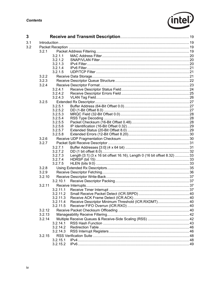
Contents 3.2.4.1 3.2.4.2 3.2.4.3 3.2.2 3.2.3 3.2.4 3.2.5 3.2.1.1 3.2.1.2 3.2.1.3 3.2.1.4 3.2.1.5 3.2.5.1 3.2.5.2 3.2.5.3 3.2.5.4 3.2.5.5 3.2.5.6 3.2.5.7 3.2.5.8 Receive and Transmit Description.................................................................... 19 Introduction................................................................................................................................. 19 Packet Reception ....................................................................................................................... 19 Packet Address Filtering............................................................................................ 19 3.2.1 MAC Address Filter...................................................................................... 20 SNAP/VLAN Filter........................................................................................ 20 IPv4 Filter..................................................................................................... 20 IPv6 Filter..................................................................................................... 21 UDP/TCP Filter ............................................................................................ 21 Receive Data Storage................................................................................................ 21 Receive Descriptor Queue Structure......................................................................... 22 Receive Descriptor Format........................................................................................ 23 Receive Descriptor Status Field................................................................... 24 Receive Descriptor Errors Field ................................................................... 25 VLAN Tag Field............................................................................................ 26 Extended Rx Descriptor............................................................................................. 27 Buffer Address (64-Bit Offset 0.0)................................................................ 27 DD (1-Bit Offset 8.0) .................................................................................... 27 MRQC Field (32-Bit Offset 0.0).................................................................... 28 RSS Type Decoding .................................................................................... 28 Packet Checksum (16-Bit Offset 0.48)......................................................... 28 IP Identification (16-Bit Offset 0.32) ............................................................. 29 Extended Status (20-Bit Offset 8.0) ............................................................. 29 Extended Errors (12-Bit Offset 8.20)............................................................ 30 Receive UDP Fragmentation Checksum................................................................... 30 Packet Split Receive Descriptor ................................................................................ 31 Buffer Addresses [3:0] (4 x 64 bit) ............................................................... 31 DD (1 bit offset 8.0)...................................................................................... 32 Length [3:1] (3 x 16 bit offset 16.16), Length 0 (16 bit offset 8.32) .............. 33 HDRSP (bit 15) ............................................................................................ 33 HLEN (bits 9:0) ............................................................................................ 33 Using Extended Rx Descriptors................................................................................. 35 Receive Descriptor Fetching...................................................................................... 36 Receive Descriptor Write-Back.................................................................................. 37 3.2.10.1 Receive Descriptor Packing......................................................................... 37 Receive Interrupts...................................................................................................... 37 3.2.11.1 Receive Timer Interrupt ............................................................................... 37 3.2.11.2 Small Receive Packet Detect (ICR.SRPD) .................................................. 40 3.2.11.3 Receive ACK Frame Detect (ICR.ACK)....................................................... 40 3.2.11.4 Receive Descriptor Minimum Threshold (ICR.RXDMT)............................... 40 3.2.11.5 Receiver FIFO Overrun (ICR.RXO) ............................................................. 40 Receive Packet Checksum Offloading ...................................................................... 40 Manageability Receive Filtering................................................................................. 42 Multiple Receive Queues & Receive-Side Scaling (RSS) ......................................... 42 3.2.14.1 RSS Hash Function ..................................................................................... 43 3.2.14.2 Redirection Table......................................................................................... 46 3.2.14.3 RSS Interrupt Registers ............................................................................... 46 RSS Verification Suite ............................................................................................... 48 IPv4.............................................................................................................. 48 IPv6.............................................................................................................. 49 3.2.7.1 3.2.7.2 3.2.7.3 3.2.7.4 3.2.7.5 3.2.15.1 3.2.15.2 3.2.6 3.2.7 3.2.8 3.2.9 3.2.10 3.2.11 3.2.12 3.2.13 3.2.14 3.2.15 3 3.1 3.2 iv
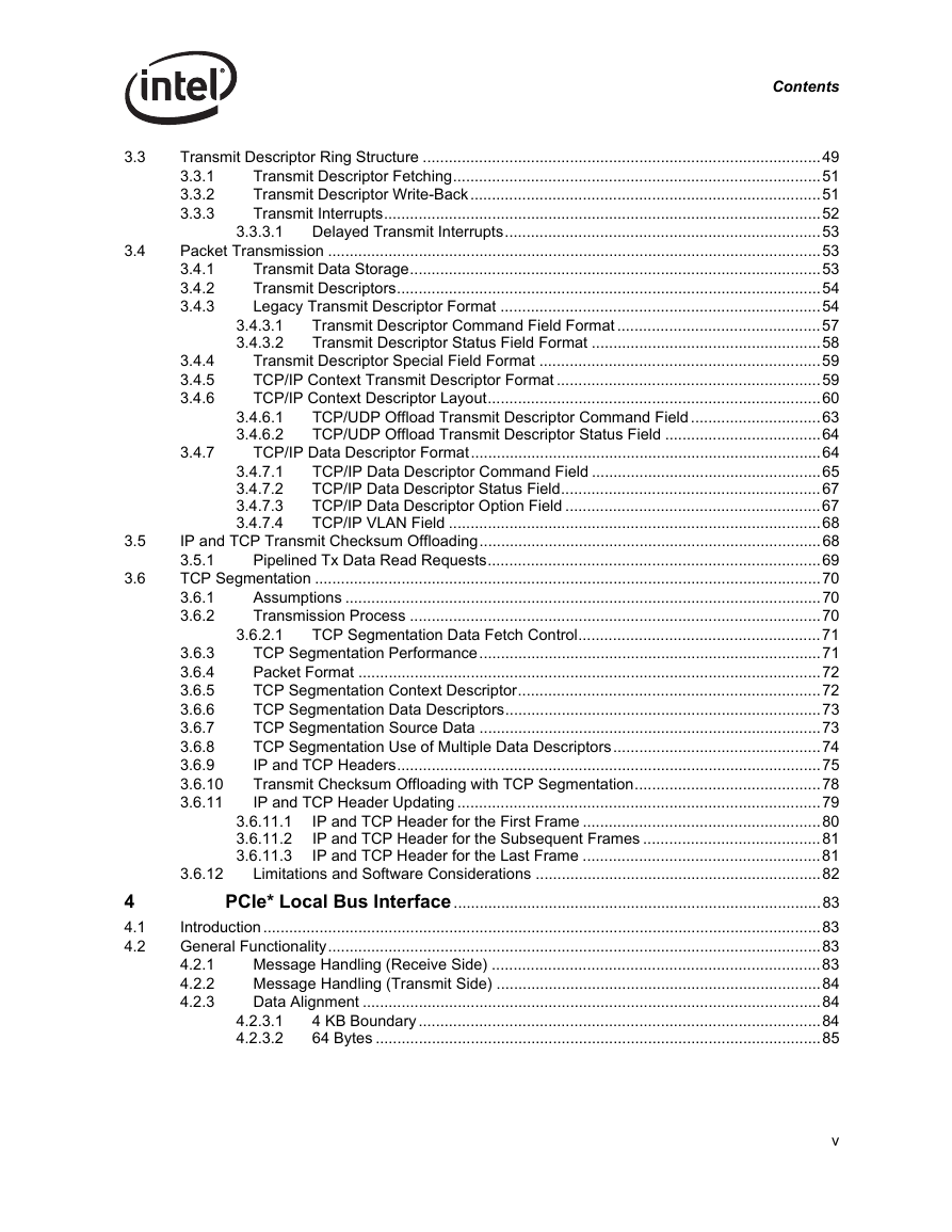
Contents 3.3 3.4 3.5 3.6 4 4.1 4.2 3.3.3.1 3.4.3.1 3.4.3.2 3.6.2.1 3.6.12 3.4.4 3.4.5 3.4.6 3.4.7 3.4.6.1 3.4.6.2 3.4.7.1 3.4.7.2 3.4.7.3 3.4.7.4 Transmit Descriptor Ring Structure ............................................................................................49 Transmit Descriptor Fetching.....................................................................................51 3.3.1 3.3.2 Transmit Descriptor Write-Back.................................................................................51 Transmit Interrupts.....................................................................................................52 3.3.3 Delayed Transmit Interrupts.........................................................................53 Packet Transmission ..................................................................................................................53 Transmit Data Storage...............................................................................................53 3.4.1 3.4.2 Transmit Descriptors..................................................................................................54 Legacy Transmit Descriptor Format ..........................................................................54 3.4.3 Transmit Descriptor Command Field Format ...............................................57 Transmit Descriptor Status Field Format .....................................................58 Transmit Descriptor Special Field Format .................................................................59 TCP/IP Context Transmit Descriptor Format .............................................................59 TCP/IP Context Descriptor Layout.............................................................................60 TCP/UDP Offload Transmit Descriptor Command Field ..............................63 TCP/UDP Offload Transmit Descriptor Status Field ....................................64 TCP/IP Data Descriptor Format.................................................................................64 TCP/IP Data Descriptor Command Field .....................................................65 TCP/IP Data Descriptor Status Field............................................................67 TCP/IP Data Descriptor Option Field ...........................................................67 TCP/IP VLAN Field ......................................................................................68 IP and TCP Transmit Checksum Offloading...............................................................................68 3.5.1 Pipelined Tx Data Read Requests.............................................................................69 TCP Segmentation .....................................................................................................................70 3.6.1 Assumptions ..............................................................................................................70 Transmission Process ...............................................................................................70 3.6.2 TCP Segmentation Data Fetch Control........................................................71 TCP Segmentation Performance...............................................................................71 Packet Format ...........................................................................................................72 TCP Segmentation Context Descriptor......................................................................72 TCP Segmentation Data Descriptors.........................................................................73 TCP Segmentation Source Data ...............................................................................73 TCP Segmentation Use of Multiple Data Descriptors................................................74 IP and TCP Headers..................................................................................................75 Transmit Checksum Offloading with TCP Segmentation...........................................78 IP and TCP Header Updating ....................................................................................79 IP and TCP Header for the First Frame .......................................................80 IP and TCP Header for the Subsequent Frames .........................................81 IP and TCP Header for the Last Frame .......................................................81 Limitations and Software Considerations ..................................................................82 PCIe* Local Bus Interface .....................................................................................83 Introduction.................................................................................................................................83 General Functionality..................................................................................................................83 Message Handling (Receive Side) ............................................................................83 4.2.1 4.2.2 Message Handling (Transmit Side) ...........................................................................84 Data Alignment ..........................................................................................................84 4.2.3 4 KB Boundary.............................................................................................84 64 Bytes .......................................................................................................85 3.6.3 3.6.4 3.6.5 3.6.6 3.6.7 3.6.8 3.6.9 3.6.10 3.6.11 3.6.11.1 3.6.11.2 3.6.11.3 4.2.3.1 4.2.3.2 v
Contents 4.2.4 4.2.4.1 4.2.4.2 4.2.4.3 Transaction Attributes................................................................................................ 85 Traffic Class and Virtual Channels............................................................... 85 Relaxed Ordering......................................................................................... 85 Snoop Not Required .................................................................................... 85 4.2.5 Error Forwarding........................................................................................................86 Flow Control ............................................................................................................................... 86 Flow Control Rules .................................................................................................... 86 4.3.1 4.3.2 Upstream Flow Control Tracking ............................................................................... 87 Flow Control Update Frequency................................................................................ 87 4.3.3 4.3.4 Flow Control Timeout Mechanism ............................................................................. 87 Host Interface ............................................................................................................................. 88 4.4.1 Tag IDs ...................................................................................................................... 88 4.4.2 Completion Timeout Mechanism ............................................................................... 89 Error Events and Error Reporting ............................................................................................... 89 Error Events............................................................................................................... 89 4.5.1 4.5.2 Error Pollution............................................................................................................ 91 4.5.3 Unsuccessful Completion Status.............................................................................. 91 Link Layer ................................................................................................................................... 92 ACK/NAK Scheme..................................................................................................... 92 4.6.1 4.6.2 Supported DLLPs ...................................................................................................... 92 4.6.3 Transmit EDB Nullifying............................................................................................. 93 Physical Layer ............................................................................................................................ 93 Link Width.................................................................................................................. 93 4.7.1 4.7.2 Polarity Inversion (82571EB/82572EI)....................................................................... 94 Lane-To-Lane De-Skew (82571EB/82572EI) ............................................................ 94 4.7.3 Lane Reversal (82571EB/82572EI)........................................................................... 94 4.7.4 Performance Monitoring ............................................................................................ 95 4.7.5 Configuration Registers ............................................................................................. 95 4.7.6 PCI Compatibility ......................................................................................... 95 Mandatory PCI Configuration Registers .................................................................... 97 UHCI Registers (631xESB/632xESB only)..............................................................109 PCI Power Management Registers .........................................................................110 4.7.9.1 Message Signaled Interrupt Configuration Registers ................................113 4.7.9.2 PCIe* Configuration Registers ...................................................................115 EEPROM/NVM Interface.......................................................................................125 Introduction...............................................................................................................................125 EEPROM Device (82571EB/82572EI/631xESB/632xESB) .....................................................126 Software Accesses ..................................................................................................126 5.2.1 Signature and CRC Fields.......................................................................................127 5.2.2 5.2.3 Protected EEPROM Space (82571EB/82572EI).....................................................127 Protected EEPROM Space (631xESB/632xESB) ...................................................127 5.2.4 Initial EEPROM Programming .................................................................................129 5.2.5 Activating the Protection Mechanism.......................................................................129 5.2.6 5.2.7 Initial EEPROM Programming .................................................................................129 EEPROM Firmware/Software Synchronization (631xESB/632xESB)......................................130 EEPROM/PHY Firmware/Software Synchronization (82571EB)..............................................131 4.7.6.1 4.7.7 4.7.8 4.7.9 4.3 4.4 4.5 4.6 4.7 5 5.1 5.2 5.3 5.4 vi
分享到:
收藏