logo资料库

蓝牙芯片DA14531 DATASHEET.pdf

第1页 / 共374页
第2页 / 共374页
第3页 / 共374页
第4页 / 共374页
第5页 / 共374页
第6页 / 共374页
第7页 / 共374页
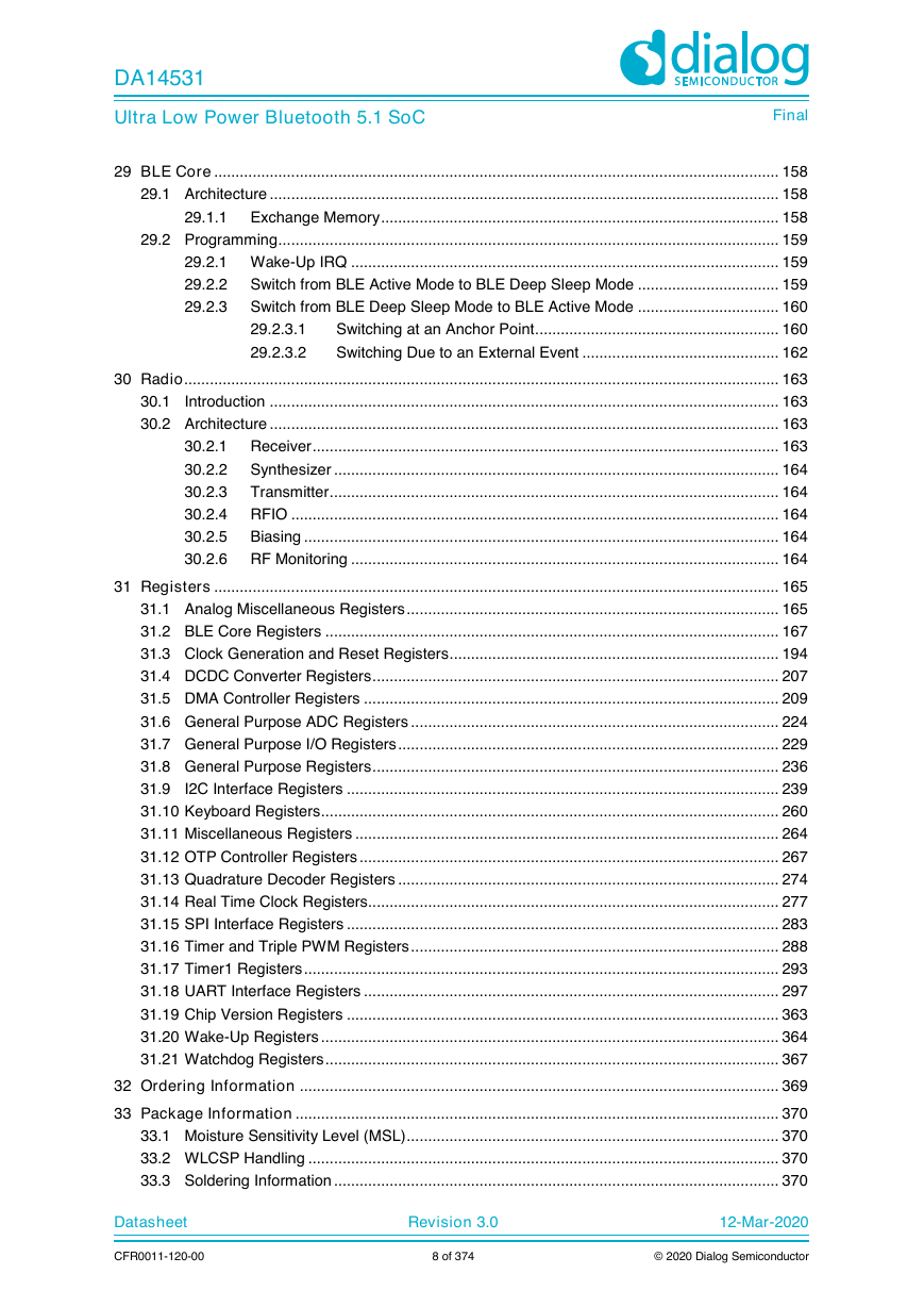
第8页 / 共374页
资料共374页,剩余部分请下载后查看
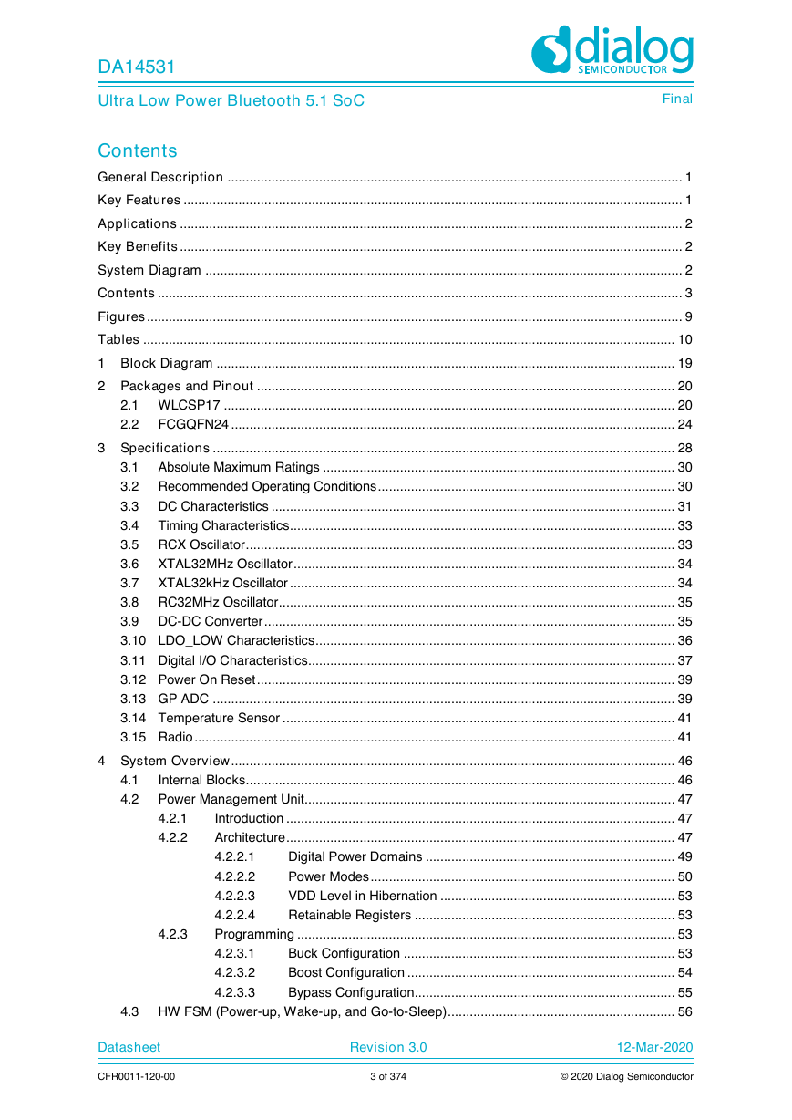
General Description
Key Features
Applications
Key Benefits
System Diagram
Contents
Figures
Tables
1 Block Diagram
2 Packages and Pinout
2.1 WLCSP17
2.2 FCGQFN24
3 Specifications
3.1 Absolute Maximum Ratings
3.2 Recommended Operating Conditions
3.3 DC Characteristics
3.4 Timing Characteristics
3.5 RCX Oscillator
3.6 XTAL32MHz Oscillator
3.7 XTAL32kHz Oscillator
3.8 RC32MHz Oscillator
3.9 DC-DC Converter
3.10 LDO_LOW Characteristics
3.11 Digital I/O Characteristics
3.12 Power On Reset
3.13 GP ADC
3.14 Temperature Sensor
3.15 Radio
4 System Overview
4.1 Internal Blocks
4.2 Power Management Unit
4.2.1 Introduction
4.2.2 Architecture
4.2.2.1 Digital Power Domains
4.2.2.2 Power Modes
4.2.2.3 VDD Level in Hibernation
4.2.2.4 Retainable Registers
4.2.3 Programming
4.2.3.1 Buck Configuration
4.2.3.2 Boost Configuration
4.2.3.3 Bypass Configuration
4.3 HW FSM (Power-up, Wake-up, and Go-to-Sleep)
4.3.1 Power-up/Wake-up in Buck Configuration
4.3.2 Power-up/Wake-up in Boost Configuration
4.3.3 Go-to-Sleep and Refresh Bandgap
4.4 OTP Memory Layout
4.4.1 OTP Header
4.4.2 Configuration Script
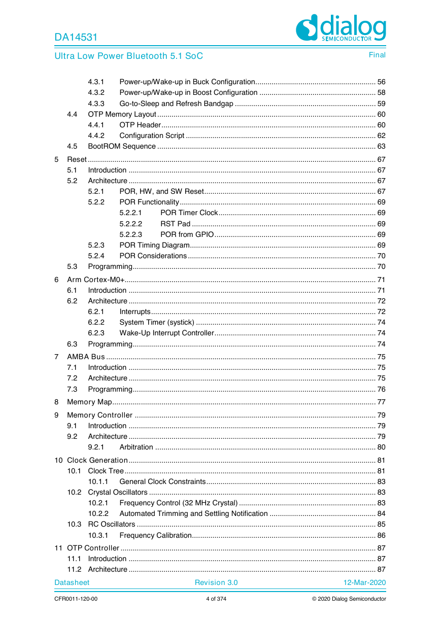
4.5 BootROM Sequence
5 Reset
5.1 Introduction
5.2 Architecture
5.2.1 POR, HW, and SW Reset
5.2.2 POR Functionality
5.2.2.1 POR Timer Clock
5.2.2.2 RST Pad
5.2.2.3 POR from GPIO
5.2.3 POR Timing Diagram
5.2.4 POR Considerations
5.3 Programming
6 Arm Cortex-M0+
6.1 Introduction
6.2 Architecture
6.2.1 Interrupts
6.2.2 System Timer (systick)
6.2.3 Wake-Up Interrupt Controller
6.3 Programming
7 AMBA Bus
7.1 Introduction
7.2 Architecture
7.3 Programming
8 Memory Map
9 Memory Controller
9.1 Introduction
9.2 Architecture
9.2.1 Arbitration
10 Clock Generation
10.1 Clock Tree
10.1.1 General Clock Constraints
10.2 Crystal Oscillators
10.2.1 Frequency Control (32 MHz Crystal)
10.2.2 Automated Trimming and Settling Notification
10.3 RC Oscillators
10.3.1 Frequency Calibration
11 OTP Controller
11.1 Introduction
11.2 Architecture
11.2.1 OTP Accessing Considerations
11.3 Programming
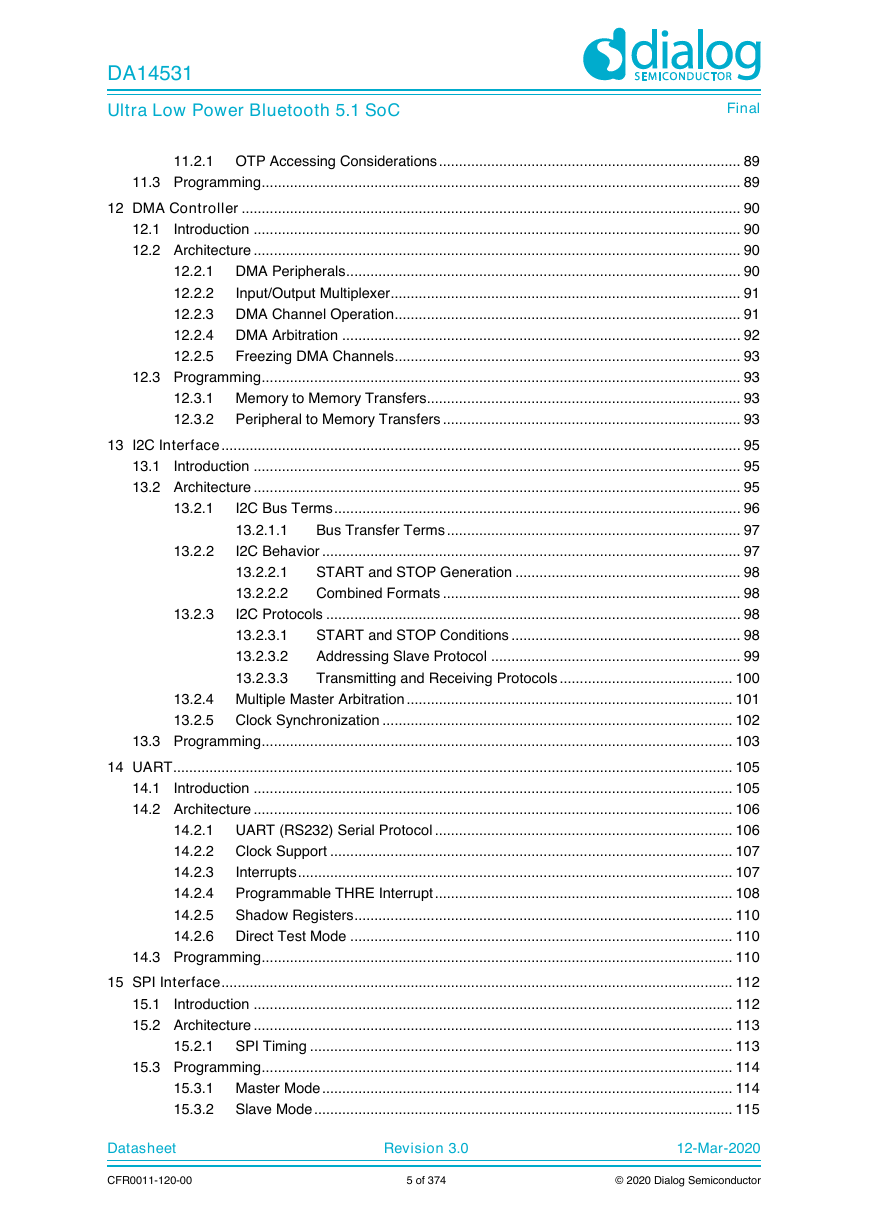
12 DMA Controller
12.1 Introduction
12.2 Architecture
12.2.1 DMA Peripherals
12.2.2 Input/Output Multiplexer
12.2.3 DMA Channel Operation
12.2.4 DMA Arbitration
12.2.5 Freezing DMA Channels
12.3 Programming
12.3.1 Memory to Memory Transfers
12.3.2 Peripheral to Memory Transfers
13 I2C Interface
13.1 Introduction
13.2 Architecture
13.2.1 I2C Bus Terms
13.2.1.1 Bus Transfer Terms
13.2.2 I2C Behavior
13.2.2.1 START and STOP Generation
13.2.2.2 Combined Formats
13.2.3 I2C Protocols
13.2.3.1 START and STOP Conditions
13.2.3.2 Addressing Slave Protocol
7-bit Address Format
10-bit Address Format
13.2.3.3 Transmitting and Receiving Protocols
Master-Transmitter and Slave-Receiver
Master-Receiver and Slave-Transmitter
START BYTE Transfer Protocol
13.2.4 Multiple Master Arbitration
13.2.5 Clock Synchronization
13.3 Programming
14 UART
14.1 Introduction
14.2 Architecture
14.2.1 UART (RS232) Serial Protocol
14.2.2 Clock Support
14.2.3 Interrupts
14.2.4 Programmable THRE Interrupt
14.2.5 Shadow Registers
14.2.6 Direct Test Mode
14.3 Programming
15 SPI Interface
15.1 Introduction
15.2 Architecture
15.2.1 SPI Timing
15.3 Programming
15.3.1 Master Mode
15.3.2 Slave Mode
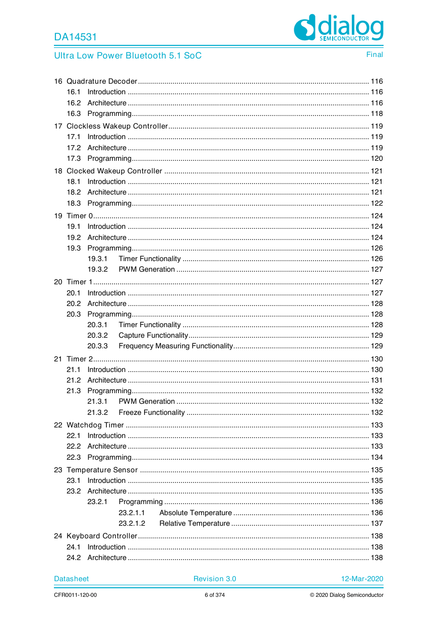
16 Quadrature Decoder
16.1 Introduction
16.2 Architecture
16.3 Programming
17 Clockless Wakeup Controller
17.1 Introduction
17.2 Architecture
17.3 Programming
18 Clocked Wakeup Controller
18.1 Introduction
18.2 Architecture
18.3 Programming
19 Timer 0
19.1 Introduction
19.2 Architecture
19.3 Programming
19.3.1 Timer Functionality
19.3.2 PWM Generation
20 Timer 1
20.1 Introduction
20.2 Architecture
20.3 Programming
20.3.1 Timer Functionality
20.3.2 Capture Functionality
20.3.3 Frequency Measuring Functionality
21 Timer 2
21.1 Introduction
21.2 Architecture
21.3 Programming
21.3.1 PWM Generation
21.3.2 Freeze Functionality
22 Watchdog Timer
22.1 Introduction
22.2 Architecture
22.3 Programming
23 Temperature Sensor
23.1 Introduction
23.2 Architecture
23.2.1 Programming
23.2.1.1 Absolute Temperature
23.2.1.2 Relative Temperature
24 Keyboard Controller
24.1 Introduction
24.2 Architecture
24.2.1 Keyboard Scanner
24.2.2 GPIO Interrupt Generator
24.3 Programming
24.3.1 Keyboard Scanner
24.3.2 GPIO Interrupts
25 Input/Output Ports
25.1 Introduction
25.2 Architecture
25.2.1 Programmable Pin Assignment
25.2.1.1 Priority
25.2.1.2 Direction Control
25.2.2 General Purpose Port Registers
25.2.2.1 Port Data Register
25.2.2.2 Port Set Data Output Register
25.2.2.3 Port Reset Data Output Register
25.2.3 Fixed Assignment Functionality
25.2.4 Types of GPIO Pads
25.2.5 Driving Strength
26 General Purpose ADC
26.1 Introduction
26.2 Architecture
26.2.1 Input Channels
26.2.2 Operating Modes
26.2.2.1 Enabling the ADC
26.2.2.2 Manual Mode
26.2.2.3 Continuous Mode
26.2.3 Conversion Modes
26.2.3.1 AD Conversion
Sampling Phase
Conversion and Storage Phase
26.2.3.2 Averaging
26.2.3.3 Chopper Mode
26.2.4 Additional Settings
26.2.5 Non-Ideal Effects
26.2.6 Offset Calibration
26.2.7 Zero-Scale Adjustment
26.2.8 Common Mode Adjustment
26.2.9 Input Impedance, Inductance, and Input Settling
26.3 Programming
27 Real Time Clock (RTC)
27.1 Introduction
27.2 Architecture
27.3 Programming
28 Power
28.1 DCDC Converter
28.2 LDOs
28.3 POR Circuit
29 BLE Core
29.1 Architecture
29.1.1 Exchange Memory
29.2 Programming
29.2.1 Wake-Up IRQ
29.2.2 Switch from BLE Active Mode to BLE Deep Sleep Mode
29.2.3 Switch from BLE Deep Sleep Mode to BLE Active Mode
29.2.3.1 Switching at an Anchor Point
29.2.3.2 Switching Due to an External Event
30 Radio
30.1 Introduction
30.2 Architecture
30.2.1 Receiver
30.2.2 Synthesizer
30.2.3 Transmitter
30.2.4 RFIO
30.2.5 Biasing
30.2.6 RF Monitoring
31 Registers
31.1 Analog Miscellaneous Registers
31.2 BLE Core Registers
31.3 Clock Generation and Reset Registers
31.4 DCDC Converter Registers
31.5 DMA Controller Registers
31.6 General Purpose ADC Registers
31.7 General Purpose I/O Registers
31.8 General Purpose Registers
31.9 I2C Interface Registers
31.10 Keyboard Registers
31.11 Miscellaneous Registers
31.12 OTP Controller Registers
31.13 Quadrature Decoder Registers
31.14 Real Time Clock Registers
31.15 SPI Interface Registers
31.16 Timer and Triple PWM Registers
31.17 Timer1 Registers
31.18 UART Interface Registers
31.19 Chip Version Registers
31.20 Wake-Up Registers
31.21 Watchdog Registers
32 Ordering Information
33 Package Information
33.1 Moisture Sensitivity Level (MSL)
33.2 WLCSP Handling
33.3 Soldering Information
33.4 Package Outlines
Revision History
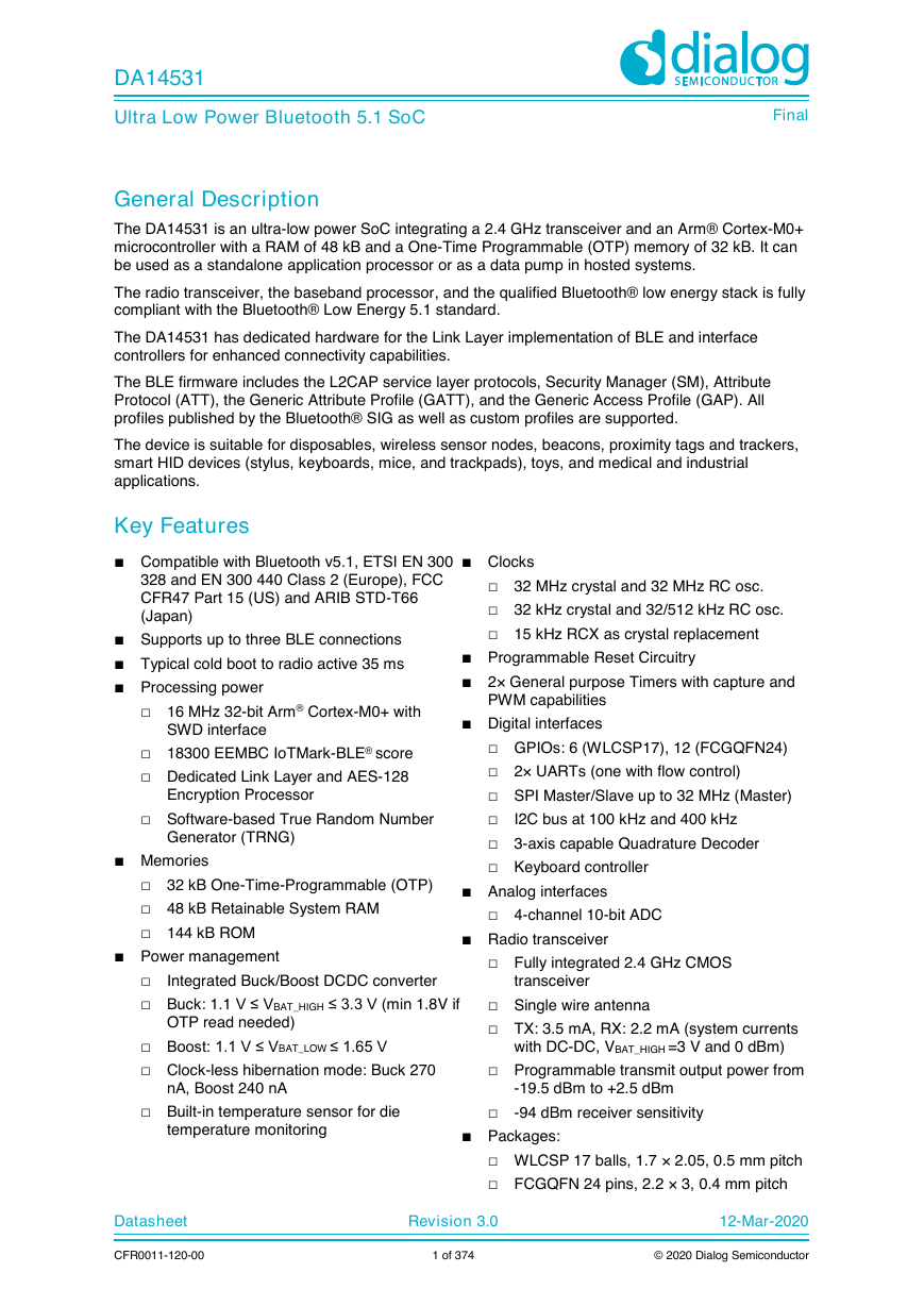
DA14531 Ultra Low Power Bluetooth 5.1 SoC General Description Final The DA14531 is an ultra-low power SoC integrating a 2.4 GHz transceiver and an Arm® Cortex-M0+ microcontroller with a RAM of 48 kB and a One-Time Programmable (OTP) memory of 32 kB. It can be used as a standalone application processor or as a data pump in hosted systems. The radio transceiver, the baseband processor, and the qualified Bluetooth® low energy stack is fully compliant with the Bluetooth® Low Energy 5.1 standard. The DA14531 has dedicated hardware for the Link Layer implementation of BLE and interface controllers for enhanced connectivity capabilities. The BLE firmware includes the L2CAP service layer protocols, Security Manager (SM), Attribute Protocol (ATT), the Generic Attribute Profile (GATT), and the Generic Access Profile (GAP). All profiles published by the Bluetooth® SIG as well as custom profiles are supported. The device is suitable for disposables, wireless sensor nodes, beacons, proximity tags and trackers, smart HID devices (stylus, keyboards, mice, and trackpads), toys, and medical and industrial applications. Key Features ■ Compatible with Bluetooth v5.1, ETSI EN 300 ■ Clocks 328 and EN 300 440 Class 2 (Europe), FCC CFR47 Part 15 (US) and ARIB STD-T66 (Japan) ■ Supports up to three BLE connections ■ Typical cold boot to radio active 35 ms ■ Processing power □ 16 MHz 32-bit Arm® Cortex-M0+ with SWD interface □ 18300 EEMBC IoTMark-BLE® □ Dedicated Link Layer and AES-128 score Encryption Processor □ Software-based True Random Number Generator (TRNG) ■ Memories □ 32 MHz crystal and 32 MHz RC osc. □ 32 kHz crystal and 32/512 kHz RC osc. □ 15 kHz RCX as crystal replacement ■ Programmable Reset Circuitry ■ 2× General purpose Timers with capture and PWM capabilities ■ Digital interfaces □ GPIOs: 6 (WLCSP17), 12 (FCGQFN24) □ 2× UARTs (one with flow control) □ SPI Master/Slave up to 32 MHz (Master) □ □ 3-axis capable Quadrature Decoder □ Keyboard controller I2C bus at 100 kHz and 400 kHz □ 32 kB One-Time-Programmable (OTP) □ 48 kB Retainable System RAM □ 144 kB ROM ■ Analog interfaces □ 4-channel 10-bit ADC ■ Radio transceiver ■ Power management Integrated Buck/Boost DCDC converter □ □ Buck: 1.1 V ≤ VBAT_HIGH ≤ 3.3 V (min 1.8V if OTP read needed) □ Boost: 1.1 V ≤ VBAT_LOW ≤ 1.65 V □ Clock-less hibernation mode: Buck 270 nA, Boost 240 nA □ Fully integrated 2.4 GHz CMOS transceiver □ Single wire antenna □ TX: 3.5 mA, RX: 2.2 mA (system currents with DC-DC, VBAT_HIGH =3 V and 0 dBm) □ Programmable transmit output power from -19.5 dBm to +2.5 dBm □ Built-in temperature sensor for die □ -94 dBm receiver sensitivity temperature monitoring ■ Packages: Datasheet CFR0011-120-00 □ WLCSP 17 balls, 1.7 × 2.05, 0.5 mm pitch □ FCGQFN 24 pins, 2.2 × 3, 0.4 mm pitch Revision 3.0 12-Mar-2020 1 of 374 © 2020 Dialog Semiconductor
DA14531 Ultra Low Power Bluetooth 5.1 SoC Final Applications ■ Medical applications ■ Disposables ■ Beacons ■ Proximity tags and trackers ■ Wireless sensor nodes □ Fitness trackers □ Consumer health ■ Smartwatches ■ Human interface devices (HID) □ Stylus pens □ Keyboards □ Mouse devices □ Trackpads ■ Toys ■ Industrial appliances Key Benefits ■ Lowest power consumption ■ Smallest system size ■ Lowest system cost System Diagram Datasheet CFR0011-120-00 Figure 1: System Diagram Revision 3.0 12-Mar-2020 2 of 374 © 2020 Dialog Semiconductor
DA14531 Ultra Low Power Bluetooth 5.1 SoC Contents Final General Description ............................................................................................................................ 1 Key Features ........................................................................................................................................ 1 Applications ......................................................................................................................................... 2 Key Benefits ......................................................................................................................................... 2 System Diagram .................................................................................................................................. 2 Contents ............................................................................................................................................... 3 Figures .................................................................................................................................................. 9 Tables ................................................................................................................................................. 10 1 Block Diagram ............................................................................................................................. 19 2 Packages and Pinout .................................................................................................................. 20 2.1 WLCSP17 ........................................................................................................................... 20 2.2 FCGQFN24 ......................................................................................................................... 24 3 Specifications .............................................................................................................................. 28 3.1 Absolute Maximum Ratings ................................................................................................ 30 3.2 Recommended Operating Conditions ................................................................................. 30 3.3 DC Characteristics .............................................................................................................. 31 3.4 Timing Characteristics ......................................................................................................... 33 3.5 RCX Oscillator ..................................................................................................................... 33 3.6 XTAL32MHz Oscillator ........................................................................................................ 34 3.7 XTAL32kHz Oscillator ......................................................................................................... 34 3.8 RC32MHz Oscillator ............................................................................................................ 35 3.9 DC-DC Converter ................................................................................................................ 35 3.10 LDO_LOW Characteristics .................................................................................................. 36 3.11 Digital I/O Characteristics.................................................................................................... 37 3.12 Power On Reset .................................................................................................................. 39 3.13 GP ADC .............................................................................................................................. 39 3.14 Temperature Sensor ........................................................................................................... 41 3.15 Radio ................................................................................................................................... 41 4.2.1 4.2.2 4 System Overview ......................................................................................................................... 46 Internal Blocks ..................................................................................................................... 46 4.1 4.2 Power Management Unit..................................................................................................... 47 Introduction .......................................................................................................... 47 Architecture .......................................................................................................... 47 Digital Power Domains .................................................................... 49 4.2.2.1 Power Modes ................................................................................... 50 VDD Level in Hibernation ................................................................ 53 Retainable Registers ....................................................................... 53 4.2.2.4 Programming ....................................................................................................... 53 Buck Configuration .......................................................................... 53 4.2.3.1 Boost Configuration ......................................................................... 54 Bypass Configuration....................................................................... 55 4.3 HW FSM (Power-up, Wake-up, and Go-to-Sleep) .............................................................. 56 4.2.2.2 4.2.2.3 4.2.3 4.2.3.2 4.2.3.3 Datasheet CFR0011-120-00 Revision 3.0 12-Mar-2020 3 of 374 © 2020 Dialog Semiconductor
DA14531 Ultra Low Power Bluetooth 5.1 SoC Final 4.3.3 4.3.1 4.3.2 Power-up/Wake-up in Buck Configuration........................................................... 56 Power-up/Wake-up in Boost Configuration ......................................................... 58 Go-to-Sleep and Refresh Bandgap ..................................................................... 59 4.4 OTP Memory Layout ........................................................................................................... 60 OTP Header ......................................................................................................... 60 Configuration Script ............................................................................................. 62 4.5 BootROM Sequence ........................................................................................................... 63 4.4.1 4.4.2 5.2.2 5.2.1 5 Reset ............................................................................................................................................. 67 Introduction ......................................................................................................................... 67 5.1 5.2 Architecture ......................................................................................................................... 67 POR, HW, and SW Reset .................................................................................... 67 POR Functionality ................................................................................................ 69 POR Timer Clock ............................................................................. 69 5.2.2.1 RST Pad .......................................................................................... 69 POR from GPIO ............................................................................... 69 5.2.2.3 POR Timing Diagram ........................................................................................... 69 POR Considerations ............................................................................................ 70 5.3 Programming ....................................................................................................................... 70 5.2.2.2 5.2.3 5.2.4 6 Arm Cortex-M0+ ........................................................................................................................... 71 Introduction ......................................................................................................................... 71 6.1 6.2 Architecture ......................................................................................................................... 72 Interrupts .............................................................................................................. 72 System Timer (systick) ........................................................................................ 74 6.2.2 6.2.3 Wake-Up Interrupt Controller ............................................................................... 74 6.3 Programming ....................................................................................................................... 74 6.2.1 7 AMBA Bus .................................................................................................................................... 75 Introduction ......................................................................................................................... 75 7.1 7.2 Architecture ......................................................................................................................... 75 7.3 Programming ....................................................................................................................... 76 8 Memory Map................................................................................................................................. 77 9 Memory Controller ...................................................................................................................... 79 Introduction ......................................................................................................................... 79 9.1 9.2 Architecture ......................................................................................................................... 79 Arbitration ............................................................................................................ 80 9.2.1 10 Clock Generation ......................................................................................................................... 81 10.1 Clock Tree ........................................................................................................................... 81 10.1.1 General Clock Constraints ................................................................................... 83 10.2 Crystal Oscillators ............................................................................................................... 83 10.2.1 Frequency Control (32 MHz Crystal) ................................................................... 83 10.2.2 Automated Trimming and Settling Notification .................................................... 84 10.3 RC Oscillators ..................................................................................................................... 85 10.3.1 Frequency Calibration .......................................................................................... 86 11 OTP Controller ............................................................................................................................. 87 Introduction ......................................................................................................................... 87 11.1 11.2 Architecture ......................................................................................................................... 87 Datasheet CFR0011-120-00 Revision 3.0 12-Mar-2020 4 of 374 © 2020 Dialog Semiconductor
DA14531 Ultra Low Power Bluetooth 5.1 SoC Final 11.2.1 OTP Accessing Considerations ........................................................................... 89 11.3 Programming ....................................................................................................................... 89 12 DMA Controller ............................................................................................................................ 90 Introduction ......................................................................................................................... 90 12.1 12.2 Architecture ......................................................................................................................... 90 12.2.1 DMA Peripherals .................................................................................................. 90 Input/Output Multiplexer....................................................................................... 91 12.2.2 12.2.3 DMA Channel Operation...................................................................................... 91 12.2.4 DMA Arbitration ................................................................................................... 92 12.2.5 Freezing DMA Channels...................................................................................... 93 12.3 Programming ....................................................................................................................... 93 12.3.1 Memory to Memory Transfers.............................................................................. 93 12.3.2 Peripheral to Memory Transfers .......................................................................... 93 13.2.1 13.2.2 13.2.3 13 I2C Interface ................................................................................................................................. 95 Introduction ......................................................................................................................... 95 13.1 13.2 Architecture ......................................................................................................................... 95 I2C Bus Terms ..................................................................................................... 96 Bus Transfer Terms ......................................................................... 97 13.2.1.1 I2C Behavior ........................................................................................................ 97 START and STOP Generation ........................................................ 98 13.2.2.1 Combined Formats .......................................................................... 98 13.2.2.2 I2C Protocols ....................................................................................................... 98 START and STOP Conditions ......................................................... 98 13.2.3.1 Addressing Slave Protocol .............................................................. 99 Transmitting and Receiving Protocols ........................................... 100 13.2.4 Multiple Master Arbitration ................................................................................. 101 13.2.5 Clock Synchronization ....................................................................................... 102 13.3 Programming ..................................................................................................................... 103 13.2.3.2 13.2.3.3 14 UART ........................................................................................................................................... 105 Introduction ....................................................................................................................... 105 14.1 14.2 Architecture ....................................................................................................................... 106 14.2.1 UART (RS232) Serial Protocol .......................................................................... 106 14.2.2 Clock Support .................................................................................................... 107 Interrupts ............................................................................................................ 107 14.2.3 14.2.4 Programmable THRE Interrupt .......................................................................... 108 14.2.5 Shadow Registers .............................................................................................. 110 14.2.6 Direct Test Mode ............................................................................................... 110 14.3 Programming ..................................................................................................................... 110 15 SPI Interface ............................................................................................................................... 112 Introduction ....................................................................................................................... 112 15.1 15.2 Architecture ....................................................................................................................... 113 15.2.1 SPI Timing ......................................................................................................... 113 15.3 Programming ..................................................................................................................... 114 15.3.1 Master Mode ...................................................................................................... 114 15.3.2 Slave Mode ........................................................................................................ 115 Datasheet CFR0011-120-00 Revision 3.0 12-Mar-2020 5 of 374 © 2020 Dialog Semiconductor
DA14531 Ultra Low Power Bluetooth 5.1 SoC Final 16 Quadrature Decoder .................................................................................................................. 116 Introduction ....................................................................................................................... 116 16.1 16.2 Architecture ....................................................................................................................... 116 16.3 Programming ..................................................................................................................... 118 17 Clockless Wakeup Controller................................................................................................... 119 Introduction ....................................................................................................................... 119 17.1 17.2 Architecture ....................................................................................................................... 119 17.3 Programming ..................................................................................................................... 120 18 Clocked Wakeup Controller ..................................................................................................... 121 Introduction ....................................................................................................................... 121 18.1 18.2 Architecture ....................................................................................................................... 121 18.3 Programming ..................................................................................................................... 122 19 Timer 0 ........................................................................................................................................ 124 Introduction ....................................................................................................................... 124 19.1 19.2 Architecture ....................................................................................................................... 124 19.3 Programming ..................................................................................................................... 126 19.3.1 Timer Functionality ............................................................................................ 126 19.3.2 PWM Generation ............................................................................................... 127 20 Timer 1 ........................................................................................................................................ 127 Introduction ....................................................................................................................... 127 20.1 20.2 Architecture ....................................................................................................................... 128 20.3 Programming ..................................................................................................................... 128 20.3.1 Timer Functionality ............................................................................................ 128 20.3.2 Capture Functionality ......................................................................................... 129 20.3.3 Frequency Measuring Functionality ................................................................... 129 21 Timer 2 ........................................................................................................................................ 130 Introduction ....................................................................................................................... 130 21.1 21.2 Architecture ....................................................................................................................... 131 21.3 Programming ..................................................................................................................... 132 21.3.1 PWM Generation ............................................................................................... 132 21.3.2 Freeze Functionality .......................................................................................... 132 22 Watchdog Timer ........................................................................................................................ 133 Introduction ....................................................................................................................... 133 22.1 22.2 Architecture ....................................................................................................................... 133 22.3 Programming ..................................................................................................................... 134 23 Temperature Sensor ................................................................................................................. 135 Introduction ....................................................................................................................... 135 23.1 23.2 Architecture ....................................................................................................................... 135 23.2.1 Programming ..................................................................................................... 136 Absolute Temperature ................................................................... 136 Relative Temperature .................................................................... 137 23.2.1.1 23.2.1.2 24 Keyboard Controller .................................................................................................................. 138 Introduction ....................................................................................................................... 138 24.1 24.2 Architecture ....................................................................................................................... 138 Datasheet CFR0011-120-00 Revision 3.0 12-Mar-2020 6 of 374 © 2020 Dialog Semiconductor
DA14531 Ultra Low Power Bluetooth 5.1 SoC Final 24.2.1 Keyboard Scanner ............................................................................................. 138 24.2.2 GPIO Interrupt Generator .................................................................................. 139 24.3 Programming ..................................................................................................................... 140 24.3.1 Keyboard Scanner ............................................................................................. 140 24.3.2 GPIO Interrupts .................................................................................................. 140 25.2.1.1 25 Input/Output Ports ..................................................................................................................... 141 Introduction ....................................................................................................................... 141 25.1 25.2 Architecture ....................................................................................................................... 141 25.2.1 Programmable Pin Assignment ......................................................................... 141 Priority ............................................................................................ 142 Direction Control ............................................................................ 142 25.2.2 General Purpose Port Registers ........................................................................ 142 Port Data Register ......................................................................... 142 Port Set Data Output Register ....................................................... 142 Port Reset Data Output Register ................................................... 142 25.2.3 Fixed Assignment Functionality ......................................................................... 142 25.2.4 Types of GPIO Pads .......................................................................................... 143 25.2.5 Driving Strength ................................................................................................. 144 25.2.1.2 25.2.2.1 25.2.2.2 25.2.2.3 26 General Purpose ADC ............................................................................................................... 145 Introduction ....................................................................................................................... 145 26.1 26.2 Architecture ....................................................................................................................... 146 Input Channels ................................................................................................... 146 26.2.1 26.2.2 Operating Modes ............................................................................................... 147 Enabling the ADC .......................................................................... 148 26.2.2.1 26.2.2.2 Manual Mode ................................................................................. 148 Continuous Mode ........................................................................... 148 26.2.2.3 26.2.3 Conversion Modes ............................................................................................. 148 AD Conversion ............................................................................... 148 Averaging ....................................................................................... 150 Chopper Mode ............................................................................... 150 26.2.4 Additional Settings ............................................................................................. 150 26.2.5 Non-Ideal Effects ............................................................................................... 151 26.2.6 Offset Calibration ............................................................................................... 151 26.2.7 Zero-Scale Adjustment ...................................................................................... 151 26.2.8 Common Mode Adjustment ............................................................................... 152 Input Impedance, Inductance, and Input Settling .............................................. 152 26.2.9 26.3 Programming ..................................................................................................................... 152 26.2.3.1 26.2.3.2 26.2.3.3 27 Real Time Clock (RTC) .............................................................................................................. 153 Introduction ....................................................................................................................... 153 27.1 27.2 Architecture ....................................................................................................................... 153 27.3 Programming ..................................................................................................................... 154 28 Power .......................................................................................................................................... 155 28.1 DCDC Converter ............................................................................................................... 155 28.2 LDOs ................................................................................................................................. 157 28.3 POR Circuit ....................................................................................................................... 157 Datasheet CFR0011-120-00 Revision 3.0 12-Mar-2020 7 of 374 © 2020 Dialog Semiconductor
DA14531 Ultra Low Power Bluetooth 5.1 SoC Final 29 BLE Core .................................................................................................................................... 158 29.1 Architecture ....................................................................................................................... 158 29.1.1 Exchange Memory ............................................................................................. 158 29.2 Programming ..................................................................................................................... 159 29.2.1 Wake-Up IRQ .................................................................................................... 159 29.2.2 Switch from BLE Active Mode to BLE Deep Sleep Mode ................................. 159 29.2.3 Switch from BLE Deep Sleep Mode to BLE Active Mode ................................. 160 Switching at an Anchor Point ......................................................... 160 Switching Due to an External Event .............................................. 162 29.2.3.1 29.2.3.2 30 Radio ........................................................................................................................................... 163 Introduction ....................................................................................................................... 163 30.1 30.2 Architecture ....................................................................................................................... 163 30.2.1 Receiver ............................................................................................................. 163 30.2.2 Synthesizer ........................................................................................................ 164 30.2.3 Transmitter ......................................................................................................... 164 30.2.4 RFIO .................................................................................................................. 164 30.2.5 Biasing ............................................................................................................... 164 30.2.6 RF Monitoring .................................................................................................... 164 31 Registers .................................................................................................................................... 165 31.1 Analog Miscellaneous Registers ....................................................................................... 165 31.2 BLE Core Registers .......................................................................................................... 167 31.3 Clock Generation and Reset Registers ............................................................................. 194 31.4 DCDC Converter Registers ............................................................................................... 207 31.5 DMA Controller Registers ................................................................................................. 209 31.6 General Purpose ADC Registers ...................................................................................... 224 31.7 General Purpose I/O Registers ......................................................................................... 229 31.8 General Purpose Registers ............................................................................................... 236 I2C Interface Registers ..................................................................................................... 239 31.9 31.10 Keyboard Registers ........................................................................................................... 260 31.11 Miscellaneous Registers ................................................................................................... 264 31.12 OTP Controller Registers .................................................................................................. 267 31.13 Quadrature Decoder Registers ......................................................................................... 274 31.14 Real Time Clock Registers................................................................................................ 277 31.15 SPI Interface Registers ..................................................................................................... 283 31.16 Timer and Triple PWM Registers ...................................................................................... 288 31.17 Timer1 Registers ............................................................................................................... 293 31.18 UART Interface Registers ................................................................................................. 297 31.19 Chip Version Registers ..................................................................................................... 363 31.20 Wake-Up Registers ........................................................................................................... 364 31.21 Watchdog Registers .......................................................................................................... 367 32 Ordering Information ................................................................................................................ 369 33 Package Information ................................................................................................................. 370 33.1 Moisture Sensitivity Level (MSL) ....................................................................................... 370 33.2 WLCSP Handling .............................................................................................................. 370 33.3 Soldering Information ........................................................................................................ 370 Datasheet CFR0011-120-00 Revision 3.0 12-Mar-2020 8 of 374 © 2020 Dialog Semiconductor
分享到:
收藏