logo资料库

Security Reference Manual for i.MX.pdf

第1页 / 共648页
第2页 / 共648页
第3页 / 共648页
第4页 / 共648页
第5页 / 共648页
第6页 / 共648页
第7页 / 共648页
第8页 / 共648页
资料共648页,剩余部分请下载后查看
Chapter 1: Security Overview
Chapter overview
Feature summary
TrustZone architecture
High Assurance Boot (HAB)
HAB process flow
HAB feature summary
Secure Non-volatile Storage Module (SNVS)
SNVS architecture
Cryptographic Acceleration And Assurance Module (CAAM)
OCOTP_CTRL
Central Security Unit (CSU)
AHB to IP Peripheral Bridge (AIPSTZ)
Digital Transmission Content Protection (DTCP)
High-bandwidth Digital Content Protection (HDCP)
System JTAG Controller (SJC)
Scan protection
TrustZone Address Space Controller (TZASC-PL380)
Smart Direct Memory Access Controller (SDMA)
TrustZone Watchdog (TZ WDOG)
Chapter 2: Security System Integration
Master ID allocation
System-level SNVS connections
Unsupported SNVS functions
SNVS clock tamper input
System security violation alarm signals monitored by SNVS
Security access error
OCRAM TrustZone support
WatchDOG mechanism
Security configuration
Field return for retest procedure
Chapter 3: Central Security Unit (CSU)
Overview
Features
Functional description
Peripheral access policy
Initialization policy
Programmable Registers
CSU
CSU_CSLn
CSU_HP0
CSU_HP1
CSU_SA
CSU_HPCONTROL0
CSU_HPCONTROL1
Chapter 4: System Boot
Overview
Boot modes
Boot mode pin settings
High level boot sequence
Boot From Fuses Mode (BOOT_MODE[1:0] = 00b)
Serial Downloader
Internal Boot Mode (BOOT_MODE[1:0] = 0b10)
Boot security settings
Device Configuration
Boot eFUSE Descriptions
GPIO Boot Overrides
Device Configuration Data
Device Initialization
Internal ROM /RAM memory map
Boot Block Activation
Clocks at Boot Time
Enabling MMU and Caches
Exception Handling
Interrupt Handling During Boot
Persistent Bits
Boot Devices (Internal Boot)
NOR Flash/OneNAND using EIM Interface
NOR Flash Boot Operation
OneNAND Flash Boot Operation
IOMUX Configuration for EIM Devices
NAND Flash
NAND eFUSE Configuration
NAND Flash Boot Flow and Boot Control Blocks (BCB)
Firmware Configuration Block
Discovered Bad Block Table
Bad Block Handling in the ROM
Toggle Mode DDR NAND Boot
GPMI and BCH Clocks Configuration
Setup DMA for DDR Transfers
Reconfigure Timing and Speed Using Values in FCB
Typical NAND Page Organization
BCH ECC Page Organization
Metadata
IOMUX Configuration for NAND
Expansion Device
Expansion Device eFUSE Configuration
MMC and eMMC Boot
SD, eSD and SDXC
IOMUX Configuration for SD/MMC
Redundant Boot Support for Expansion Device
Hard Disk and SSD
Hard Disk and SSD eFUSE Configuration
IOMUX and Timing Configuration for SATA
Redundant Boot Support for Hard Disk and SSD
Serial ROM through SPI and I2C
Serial ROM eFUSE Configuration
I2C Boot
I2C IOMUX Pin Configuration
ECSPI Boot
ECSPI IOMUX Pin Configuration
Program image
Image Vector Table and Boot Data
Image Vector Table Structure
Boot Data Structure
Device Configuration Data (DCD)
Write Data Command
Check Data Command
NOP Command
Unlock Command
Plugin Image
Serial Downloader
USB
USB Configuration Details
IOMUX Configuration for USB
Serial Download protocol
SDP Command
READ REGISTER
WRITE REGISTER
WRITE_FILE
ERROR_STATUS
DCD WRITE
JUMP ADDRESS
Recovery Devices
USB Low Power Boot
High Assurance Boot (HAB)
ROM Vector Table Addresses
Chapter 5: Cryptographic Acceleration and Assurance Module (CAAM)
Overview of CAAM ( cryptographic acceleration and assurance module) functionality
Feature summary
CAAM implementation
CAAM submodules
Cryptographic engines implemented in CAAM
CAAM modes of operation
Security Monitor security states
The effect of security state on volatile keys
The effect of security state on non-volatile keys
Keys available in different security modes
Keys available in trusted mode
Keys available in secure mode
Keys available in non-secure mode
Keys available in fail mode
CAAM hardware functional description
Buses
DMA interface (AXI master bus)
DMA bursts that may read past the end of data structures
Secure memory interface (AXI slave bus)
Register interface (IP bus)
Job execution interfaces
Job ring interface
Configuring and managing the input/output rings overview
Managing the input rings
Managing the output rings
Controlling access (rings)
Order of job completion
Initializing job rings
Asserting job ring interrupts
Executing job descriptors in single-step mode
Job scheduling
Job termination status/error codes
Job execution hardware
Descriptor controller (DECO) and cryptographic control block (CCB)
Alignment blocks
Cryptographic hardware accelerators (CHAs) (overview)
Descriptors and descriptor commands
Job descriptors
Trusted descriptors
Shared descriptors
Executing shared descriptors in proper order
Specifying different types of shared descriptor sharing
Error sharing
Changing shared descriptors
Using in-line descriptors
Using replacement job descriptors
Scatter/gather tables (SGTs)
Using descriptor commands
Command execution order
Executing commands when SHR = 0
Executing commands when SHR = 1
Executing commands when REO = 0
Executing commands when REO = 1
Executing additional HEADER commands
Jumping to another job descriptor
Command properties
Blocking commands
Load/store checkpoint
Done checkpoint
Command types
SEQ vs non-SEQ commands
Creating a sequence
Using sequences for fixed and variable length data
Transferring meta data
Rewinding a sequence
Information FIFO entries
Cryptographic class
Address pointers
HEADER command
KEY commands
LOAD commands
FIFO LOAD command
Bit length data
FIFO LOAD input data type
STORE command
FIFO STORE command
MOVE and MOVE_LEN commands
ALGORITHM OPERATION command
PROTOCOL OPERATION commands
SIGNATURE command
JUMP (HALT) command
Jump type
Local conditional jump
Non-local conditional jump
Conditional halt
Conditional halt with user-specified status
Conditional subroutine call
Conditional subroutine return
Test type
JSL and TEST CONDITION fields
JUMP command format
MATH command
SEQ IN PTR command
SEQ OUT PTR command
Cryptographic hardware accelerators (CHAs)
ARC-4 hardware accelerator (AFHA) CHA functionality
AFHA use of the Mode Register
AFHA use of the Context Register
AFHA use of the Key Register
AFHA use of the Data Size Register
Save and restore operations in AFHA Sbox and AFHA context data
What is the Sbox?
What are the I and J context pointers?
Sbox and context data operations
ARC-4 operation considerations
Data encryption standard accelerator (DES) functionality
DESA use of the Mode Register
DESA use of the Key Register
DESA use of the Key Size Register
DESA use of the Data Size Register
DESA Context Register
Save and store operations in DESA context data
Random-number generator (RNG) functionality
RNG features summary
RNG functional description
RNG state handles
RNG NIST certification
RNG operations
RNG use of the Key Registers
RNG use of the Context Register
RNG use of the Data Size Register
Message digest hardware accelerator (MDHA) functionality
MDHA use of the Mode Register
MDHA use of the Key Register
Using the MDHA Key Register with normal keys
Using the MDHA Key Register with IPAD/OPAD "split keys"
Definition and function of IPAD/OPAD split keys
Process flow of using the Key Register with split keys
Using padding with the split key type to align with storage
Length of a split key
Loading/storing a split key with a key command
Loading/storing a split key with a FIFO STORE command
Sizes of split keys
Constructing an HMAC-SHA-1 split key in memory
MDHA use of the Key Size Register
MDHA use of the Data Size Register
MDHA use of the Context Register
Save and restore operations in MDHA context data
AES accelerator (AESA) functionality
What is the AES?
Differences between the encrypt and decrypt keys
AESA modes of operation
AESA use of registers
AESA use of the parity bit
AES ECB mode
AES ECB mode use of the Mode Register
AES ECB mode use of the Context Register
AES ECB Mode use of the Data Size Register
AES ECB Mode use of the Key Register
AES ECB Mode use of the Key Size Register
AES CBC, OFB, CFB128 modes
AES CBC, OFB, and CFB128 modes use of the Mode Register
AES CBC, OFB, and CFB128 modes use of the Context Register
AES CBC, OFB, and CFB128 modes use of the Data Size Register
AES CBC, OFB, and CFB128 modes use of the Key Register
AES CBC, OFB, and CFB128 modes use of the Key Size Register
AES CTR mode
AES CTR mode use of the Mode Register
AES CTR mode use of the Context Register
AES CTR mode use of the Data Size Register
AES CTR mode use of the Key Register
AES CTR mode use of the Key Size Register
AES XCBC-MAC and CMAC modes
AES XCBC-MAC and CMAC modes use of the Mode Register
AES XCBC-MAC and CMAC Modes use of the Context Register
AES XCBC-MAC and CMAC modes use of the Class 1 ICV Size Register
AES XCBC-MAC and CMAC modes use of the Data Size Register
AES XCBC-MAC and CMAC modes use of the Key Register
AES XCBC-MAC and CMAC modes use of the Key Size Register
ICV checking in AES XCBC-MAC and CMAC modes
AESA CCM mode
Generation encryption
Decryption verification
AES CCM mode use of the Mode Register
AES CCM mode use of the Context Register
AES CCM mode use of the Data Size Register
AES CCM mode use of the Key Register
AES CCM mode use of the Key Size Register
AES CCM mode use of the ICV check
Trust Architecture modules
Secure key module functionality
Initializing and clearing black and trusted descriptor keys
Black keys and JDKEK/TDKEK
Trusted descriptors and TDSK
Master key and blobs
Black keys
Black key encapsulation schemes
Differences between black and red keys
Loading red keys
Loading black keys
Avoiding errors when loading red and black keys
Encapsulating and decapsulating black keys
Types of black keys and their use
Types of blobs for key storage
Trusted descriptors
Why trusted descriptors are needed
Trusted-descriptor key types and uses
Trusted descriptors encrypting/decrypting black keys
Trusted-descriptor blob types and uses
Trusted descriptors and secure memory
Configuring the system to create trusted descriptors properly
Creating trusted descriptors
Trusted descriptors and descriptor-header bits
Trusted-descriptor execution considerations
Using master identifier (MID) to access other memory areas
Blobs
Blob protocol
Why blobs are needed
Blob conformance considerations
Encapsulating and decapsulating blobs
Blob types
Blob types differentiated by format
Blob types differentiated by content
Red blobs (for general data)
Black blobs (for cryptographic keys)
Enforcing blob content type
Blob types differentiated by security state
Blob types differentiated by memory type
General/secure memory blobs and access control
Differences between general memory and secure memory blobs
Blob encapsulation
Blob decapsulation
Operations
Critical security parameters
Secure memory
CAAM secure memory features
Secure memory controller (SMC) states
SMC initialize state
SMC normal state
SMC fail state
Secure memory organization
Secure memory security functions
Automatic RAM zeroization
Zeroizing secure memory marked "CSP"
Access control
Access control in secure memory RAM partitions
Access control through job rings
Setting access control permissions
Cryptographic protection of exported data
Exporting/importing memory type blobs
Access permissions cryptographically bound to secure memory blobs
Initializing secure memory
Chapter 6: Secure Non-Volatile Storage (SNVS)
SNVS overview
SNVS feature summary
SNVS structure
SNVS _HP (high power part)
System security monitor (SSM)
Transitioning among system security monitor states
HP security violation policy
SNVS _HP violation sources
Master key control
Error Code for the OTPMK
Generating the code bits
Checking the code bits
Error code for the ZMK
ZMK hardware programming mechanism
Non-secure real time counter
Calibrating the time counter
Time counter alarm
Periodic interrupt
Low power part (SNVS _LP)
Behavior during system power down
Zeroizable master key (ZMK)
Secure real time counter (SRTC)
Calibrating the SRTC time counter
Time counter alarm (zmk)
Monotonic counter (MC)
Power glitch detector (PGD)
General-Purpose Register
LP security violation/tamper policy
Modes of operation
Operational states
SNVS clock sources
SNVS reset and system power up
SNVS interrupts, alarms, and security violations
Programming Guidelines
RTC/SRTC control bits setting
RTC/SRTC value read
ZMK programming guidelines
General initialization guidelines
SNVS Memory Map/Register Definition
SNVS
SNVS_HPLR
SNVS_HPCOMR
SNVS_HPCR
SNVS_HPSICR
SNVS_HPSVCR
SNVS_HPSR
SNVS_HPSVSR
SNVS_HPHACIVR
SNVS_HPHACR
SNVS_HPRTCMR
SNVS_HPRTCLR
SNVS_HPTAMR
SNVS_HPTALR
SNVS_LPLR
SNVS_LPCR
SNVS_LPMKCR
SNVS_LPSVCR
SNVS_LPTGFCR
SNVS_LPTDCR
SNVS_LPSR
SNVS_LPSRTCMR
SNVS_LPSRTCLR
SNVS_LPTAR
SNVS_LPSMCMR
SNVS_LPSMCLR
SNVS_LPPGDR
SNVS_LPGPR
SNVS_LPZMKRn
SNVS_HPVIDR1
SNVS_HPVIDR2
Appendix A: Cryptographic Acceleration and Assurance Module (CAAM) Glossary
Acronyms and abbreviations
Glossary
Appendix B: CAAM Register Descriptions
B.1 CAAM memory map/register definition
B.1.1 Memory Map
B.1.2 Register Summary
B.1.3 Register Summary
B.2 Register Definitions
B.2.1 Configuration and Special Key Registers
B.2.1.1 Master Configuration Register (MCFGR)
B.2.1.2 Security Configuration Register (SCFGR)
B.2.1.3 Job Ring MID Register (JRMIDR)
B.2.1.4 DECO Request Register (DECORR)
B.2.1.5 DECO MID Register (DECOxMID)
B.2.1.6 DECO Availability Register (DAR)
B.2.1.7 DECO Reset Register (DRR)
B.2.1.8 Job Descriptor Key Encryption Key Register (JDKEKR)
B.2.1.9 Trusted Descriptor Key Encryption Key Register (TDKEKR)
B.2.1.10 Trusted Descriptor Signing Key Register (TDSKR)
B.2.1.11 Secure Key Nonce Register (SKNR)
B.2.2 RNG Registers
B.2.2.1 RNG TRNG Miscellaneous Control Register (RTMCTL)
B.2.2.2 RNG TRNG Statistical Check Miscellaneous Register (RTSCMISC)
B.2.2.3 RNG TRNG Poker Range Register (RTPKRRNG)
B.2.2.4 RNG TRNG Poker Maximum Limit Register (RTPKRMAX)
B.2.2.5 RNG TRNG Poker Square Calculation Result Register (RTPKRSQ)
B.2.2.6 RNG TRNG Seed Control Register (RTSDCTL)
B.2.2.7 RNG TRNG Sparse Bit Limit Register (RTSBLIM)
B.2.2.8 RNG TRNG Total Samples Register (RTTOTSAM)
B.2.2.9 RNG TRNG Frequency Count Minimum Limit Register (RTFRQMIN)
B.2.2.10 RNG TRNG Frequency Count Maximum Limit Register (RTFRQMAX)
B.2.2.11 RNG TRNG Frequency Count Register (RTFRQCNT)
B.2.2.12 RNG TRNG Statistical Check Monobit Limit Register (RTSCML)
B.2.2.13 RNG TRNG Statistical Check Monobit Count Register (RTSCMC)
B.2.2.14 RNG TRNG Statistical Check Run Length 1 Limit Register (RTSCR1L)
B.2.2.15 RNG TRNG Statistical Check Run Length 1 Count Register (RTSCR1C)
B.2.2.16 RNG TRNG Statistical Check Run Length 2 Limit Register (RTSCR2L)
B.2.2.17 RNG TRNG Statistical Check Run Length 2 Count Register (RTSCR2C)
B.2.2.18 RNG TRNG Statistical Check Run Length 3 Limit Register (RTSCR3L)
B.2.2.19 RNG TRNG Statistical Check Run Length 3 Count Register (RTSCR3C)
B.2.2.20 RNG TRNG Statistical Check Run Length 4 Limit Register (RTSCR4L)
B.2.2.21 RNG TRNG Statistical Check Run Length 4 Count Register (RTSCR4C)
B.2.2.22 RNG TRNG Statistical Check Run Length 5 Limit Register (RTSCR5L)
B.2.2.23 RNG TRNG Statistical Check Run Length 5 Count Register (RTSCR5C)
B.2.2.24 RNG TRNG Statistical Check Run Length 6+ Limit Register (RTSCR6PL)
B.2.2.25 RNG TRNG Statistical Check Run Length 6+ Count Register (RTSCR6PC)
B.2.2.26 RNG TRNG Status Register (RTSTATUS)
B.2.2.27 RNG TRNG Entropy Read Registers (RTENT0 - RTENT11)
B.2.2.28 RNG TRNG Statistical Check Poker Count 1 and 0 Register (RTPKRCNT10)
B.2.2.29 RNG TRNG Statistical Check Poker Count 3 and 2 Register (RTPKRCNT32)
B.2.2.30 RNG TRNG Statistical Check Poker Count 5 and 4 Register (RTPKRCNT54)
B.2.2.31 RNG TRNG Statistical Check Poker Count 7 and 6 Register (RTPKRCNT76)
B.2.2.32 RNG TRNG Statistical Check Poker Count 9 and 8 Register (RTPKRCNT98)
B.2.2.33 RNG TRNG Statistical Check Poker Count B and A Register (RTPKRCNTBA)
B.2.2.34 RNG TRNG Statistical Check Poker Count D and C Register (RTPKRCNTDC)
B.2.2.35 RNG TRNG Statistical Check Poker Count F and E Register (RTPKRCNTFE)
B.2.2.36 RNG DRNG Status Register (RDSTA)
B.2.2.37 RNG DRNG State Handle 0 Reseed Interval Register (RDINT0)
B.2.2.38 RNG DRNG State Handle 1 Reseed Interval Register (RDINT1)
B.2.2.39 RNG DRNG Hash Control Register (RDHCNTL)
B.2.2.40 RNG DRNG Hash Digest Register (RDHDIG)
B.2.2.41 RNG DRNG Hash Buffer (RDHBUF)
B.2.3 Job Queue Controller Debugging Registers
B.2.3.1 Holding Tank Job Descriptor Address Register (HTx_JD_ADDR)
B.2.3.2 Holding Tank Shared Descriptor Address Register (HTx_SD_ADDR)
B.2.3.3 Holding Tank Job Queue Control Debug Register (HTx_JQCTRL)
B.2.3.4 Holding Tank Status Register (HTx_STATUS)
B.2.3.5 Job Ring Address-Array Address Registers (JRAAAx)
B.2.3.6 Job Ring Address-Array Valid/Source Register (JRAAVS)
B.2.3.7 Job Ring Job IDs in Use Register (JRJIDU)
B.2.3.8 Job Ring Job-Done Job ID FIFO (JRJDJIFx)
B.2.3.9 Job Ring Job-Done Source FIFO (JRJDSFx)
B.2.3.10 Job Ring Job-Done Valid FIFO (JRJDVF)
B.2.3.11 Job Ring Job-Done Status Register (JRJDS)
B.2.4 Job Ring Job-Done Descriptor Address Registers (JRJDDAx)
B.2.5 Fault and Version ID Registers
B.2.5.1 CHA Revision Number Register (CRNR)
B.2.5.2 Compile Time Parameters Register (CTPR)
B.2.5.3 Secure Memory Status Register (SMSTA)
B.2.5.4 Secure Memory Partition Owner Register (SMPO)
B.2.5.5 Fault Address Register (FAR)
B.2.5.6 Fault Address Detail Register (FADR)
B.2.5.7 CAAM Status Register (CSTA)
B.2.5.8 Secure Memory Version ID Register (SMVID)
B.2.5.9 CCB Version ID Register (CCBVID)
B.2.5.10 CHA Version ID Register (CHAVID)
B.2.5.11 CHA Number Register (CHANUM)
B.2.5.12 CAAM Version ID Register (CAAMVID)
B.2.6 Job Ring Registers
B.2.6.1 Input Ring Base Address Register (IRBAR)
B.2.6.2 Input Ring Size Register (IRSR)
B.2.6.3 Input Ring Slots Available Register (IRSAR)
B.2.6.4 Input Ring Jobs Added Register (IRJAR)
B.2.6.5 Output Ring Base Address Register (ORBAR)
B.2.6.6 Output Ring Size Register (ORSR)
B.2.6.7 Output Ring Jobs Removed Register (ORJRR)
B.2.6.8 Output Ring Slots Full Register (ORSFR)
B.2.6.9 Job Ring Output Status Register (JRSTAR)
B.2.6.9.1 JRSTA Register SSED Field When SSRC= 0000 (No Status Source)
B.2.6.9.2 JRSTA Register SSED Field When SSRC= 0010 (CCB Status Source)
B.2.6.9.3 JRSTA Register SSED Field When SSRC = 0011 (Jump Halt User Status Source)
B.2.6.9.4 JRSTA Register SSED Field When SSRC = 0100 (DECO Status Source)
B.2.6.9.5 JRSTA Register SSED Field When SSRC=0110 (Job Ring Status Source)
B.2.6.9.6 JRSTA Register SSED Field When SSRC=0111 (Jump Halt Condition Codes Source)
B.2.6.10 Job Ring Interrupt Status Register (JRINTR)
B.2.6.11 Job Ring Configuration Register (JRCFGR)
B.2.6.12 Input Ring Read Index Register (IRRIR)
B.2.6.13 Output Ring Write Index Register (ORWIR)
B.2.6.14 Job Ring Command Register (JRCR)
B.2.7 Secure Memory Registers
B.2.7.1 Secure Memory Command Register (SMCJRx)
B.2.7.2 Secure Memory Command Status Register (SMCSJRx)
B.2.7.3 Secure Memory Access Permissions Register (SMJR)
B.2.7.4 Secure Memory Access Groups Registers (SMAG2/1JR)
B.2.8 DECO and CCB Registers
B.2.8.1 Class 1 Mode Register (CxC1MR)
B.2.8.1.1 Class 1 Mode Register Field Descriptions
B.2.8.2 Class 1 Key Size Register (CxC1KSR)
B.2.8.3 Class 1 Data Size Register (CxC1DSR)
B.2.8.4 Class 1 ICV Size Register (CxC1ICVSR)
B.2.8.5 CHA Control Register (CCTRL)
B.2.8.6 IRQ Control Register (CxCIRQ)
B.2.8.7 Clear Written Register (CxCWR)
B.2.8.8 CCB Status and Error Register (CxCSTA)
B.2.8.9 AAD Size Register (CxAADSZR)
B.2.8.10 Class 1 Context Register (CxC1CTXR)
B.2.8.11 Class 1 Key Register (CxC1KEYR)
B.2.8.12 Class 2 Mode Register (CxC2MR)
B.2.8.13 Class 2 Key Size Register (CxC2KSR)
B.2.8.14 Class 2 Data Size Register (CxC2DSR)
B.2.8.15 Class 2 ICV Size Register (CxC2ICVSZR)
B.2.8.16 Class 2 Context Register (CxC2CTXR)
B.2.8.17 Class 2 Key Register (CxC2KEYR)
B.2.8.18 iNformation FIFO (CxNFIFO)
B.2.8.19 Input Data FIFO (CxIFIFO)
B.2.8.20 Output Data FIFO (CxOFIFO)
B.2.8.21 DECO Job Queue Control Register (DxJQCR)
B.2.8.22 DECO Descriptor Address Register (DxDAR)
B.2.8.23 DECO Operation Status Register (DxOPSTA)
B.2.8.24 Math Registers (DxMTH0, DxMTH1, DxMTH2 and DxMTH3)
B.2.8.25 Gather Table Register (DxGTR) and Scatter Table Register (DxSTR)
B.2.8.26 Descriptor Buffer (DxDESB)
B.2.8.27 DECOx DBG_JOB_REG (DxDJR)
B.2.8.28 DECOx DBG_DBG_REG (DxDDR)
B.2.8.29 DECOx DBG_JOB_PTR (DxDJP)
B.2.8.30 DECOx DBG_SHR_PTR (DxSDP)
B.2.8.31 DECOx DBG_MID_REG (DxDMR)
B.2.8.32 Sequence Out Length (SOL) Register
B.2.8.33 Variable Sequence Out Length (VSOL) Register
B.2.8.34 Sequence In Length (SIL) Register
B.2.8.35 Variable Sequence In Length (VSIL) Register
Security Reference Manual for i.MX 6Dual, 6Quad, 6Solo, and 6DualLite Families of Applications Processors Document Number: IMX6DQ6SDLSRM Rev. 0, 03/2013
Security Reference Manual for i.MX 6Dual, 6Quad, 6Solo, and 6DualLite Families of Applications Processors, Rev. 0, 03/2013 2 Freescale Semiconductor, Inc.
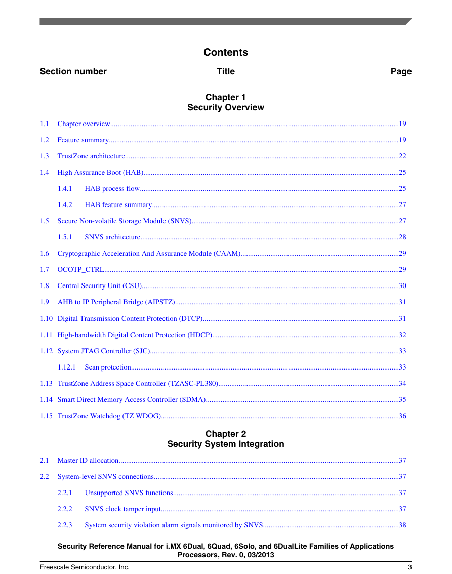
Section number Contents Title Chapter 1 Security Overview Page 1.1 Chapter overview............................................................................................................................................................19 1.2 Feature summary.............................................................................................................................................................19 1.3 TrustZone architecture....................................................................................................................................................22 1.4 High Assurance Boot (HAB)..........................................................................................................................................25 1.4.1 HAB process flow............................................................................................................................................25 1.4.2 HAB feature summary.....................................................................................................................................27 1.5 Secure Non-volatile Storage Module (SNVS)................................................................................................................27 1.5.1 SNVS architecture............................................................................................................................................28 1.6 Cryptographic Acceleration And Assurance Module (CAAM).....................................................................................29 1.7 OCOTP_CTRL...............................................................................................................................................................29 1.8 Central Security Unit (CSU)...........................................................................................................................................30 1.9 AHB to IP Peripheral Bridge (AIPSTZ).........................................................................................................................31 1.10 Digital Transmission Content Protection (DTCP)..........................................................................................................31 1.11 High-bandwidth Digital Content Protection (HDCP).....................................................................................................32 1.12 System JTAG Controller (SJC)......................................................................................................................................33 1.12.1 Scan protection.................................................................................................................................................33 1.13 TrustZone Address Space Controller (TZASC-PL380).................................................................................................34 1.14 Smart Direct Memory Access Controller (SDMA)........................................................................................................35 1.15 TrustZone Watchdog (TZ WDOG)................................................................................................................................36 Chapter 2 Security System Integration 2.1 Master ID allocation.......................................................................................................................................................37 2.2 System-level SNVS connections....................................................................................................................................37 2.2.1 Unsupported SNVS functions..........................................................................................................................37 2.2.2 SNVS clock tamper input................................................................................................................................37 2.2.3 System security violation alarm signals monitored by SNVS.........................................................................38 Security Reference Manual for i.MX 6Dual, 6Quad, 6Solo, and 6DualLite Families of Applications Processors, Rev. 0, 03/2013 Freescale Semiconductor, Inc. 3
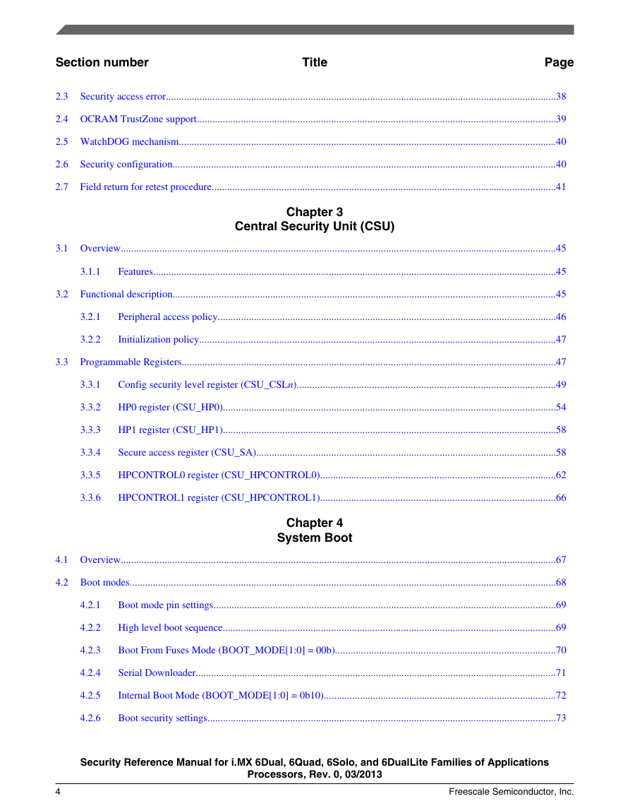
Section number Title Page 2.3 Security access error.......................................................................................................................................................38 2.4 OCRAM TrustZone support...........................................................................................................................................39 2.5 WatchDOG mechanism..................................................................................................................................................40 2.6 Security configuration.....................................................................................................................................................40 2.7 Field return for retest procedure.....................................................................................................................................41 Chapter 3 Central Security Unit (CSU) 3.1 Overview.........................................................................................................................................................................45 3.1.1 Features............................................................................................................................................................45 3.2 Functional description.....................................................................................................................................................45 3.2.1 Peripheral access policy...................................................................................................................................46 3.2.2 Initialization policy..........................................................................................................................................47 3.3 Programmable Registers.................................................................................................................................................47 3.3.1 Config security level register (CSU_CSLn)....................................................................................................49 3.3.2 HP0 register (CSU_HP0).................................................................................................................................54 3.3.3 HP1 register (CSU_HP1).................................................................................................................................58 3.3.4 Secure access register (CSU_SA)....................................................................................................................58 3.3.5 HPCONTROL0 register (CSU_HPCONTROL0)...........................................................................................62 3.3.6 HPCONTROL1 register (CSU_HPCONTROL1)...........................................................................................66 Chapter 4 System Boot 4.1 Overview.........................................................................................................................................................................67 4.2 Boot modes.....................................................................................................................................................................68 4.2.1 Boot mode pin settings.....................................................................................................................................69 4.2.2 High level boot sequence.................................................................................................................................69 4.2.3 Boot From Fuses Mode (BOOT_MODE[1:0] = 00b).....................................................................................70 4.2.4 Serial Downloader............................................................................................................................................71 4.2.5 Internal Boot Mode (BOOT_MODE[1:0] = 0b10)..........................................................................................72 4.2.6 Boot security settings.......................................................................................................................................73 Security Reference Manual for i.MX 6Dual, 6Quad, 6Solo, and 6DualLite Families of Applications Processors, Rev. 0, 03/2013 4 Freescale Semiconductor, Inc.
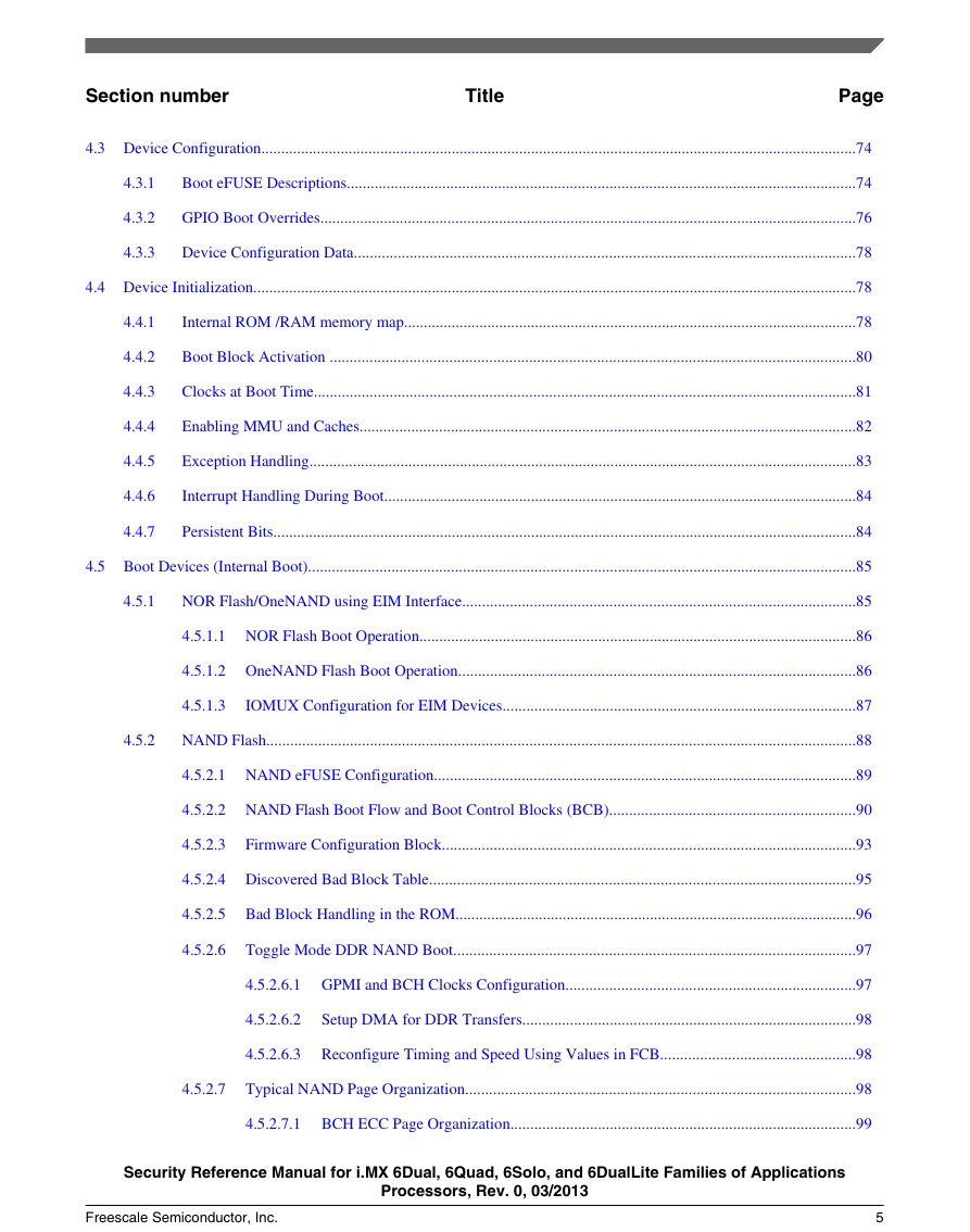
Section number Title Page 4.3 Device Configuration......................................................................................................................................................74 4.3.1 Boot eFUSE Descriptions................................................................................................................................74 4.3.2 GPIO Boot Overrides.......................................................................................................................................76 4.3.3 Device Configuration Data..............................................................................................................................78 4.4 Device Initialization........................................................................................................................................................78 4.4.1 Internal ROM /RAM memory map..................................................................................................................78 4.4.2 Boot Block Activation ....................................................................................................................................80 4.4.3 Clocks at Boot Time........................................................................................................................................81 4.4.4 Enabling MMU and Caches.............................................................................................................................82 4.4.5 Exception Handling..........................................................................................................................................83 4.4.6 Interrupt Handling During Boot.......................................................................................................................84 4.4.7 Persistent Bits...................................................................................................................................................84 4.5 Boot Devices (Internal Boot)..........................................................................................................................................85 4.5.1 NOR Flash/OneNAND using EIM Interface...................................................................................................85 4.5.1.1 NOR Flash Boot Operation..............................................................................................................86 4.5.1.2 OneNAND Flash Boot Operation....................................................................................................86 4.5.1.3 IOMUX Configuration for EIM Devices.........................................................................................87 4.5.2 NAND Flash....................................................................................................................................................88 4.5.2.1 NAND eFUSE Configuration..........................................................................................................89 4.5.2.2 NAND Flash Boot Flow and Boot Control Blocks (BCB)..............................................................90 4.5.2.3 Firmware Configuration Block........................................................................................................93 4.5.2.4 Discovered Bad Block Table...........................................................................................................95 4.5.2.5 Bad Block Handling in the ROM.....................................................................................................96 4.5.2.6 Toggle Mode DDR NAND Boot.....................................................................................................97 4.5.2.6.1 GPMI and BCH Clocks Configuration.........................................................................97 4.5.2.6.2 Setup DMA for DDR Transfers....................................................................................98 4.5.2.6.3 Reconfigure Timing and Speed Using Values in FCB.................................................98 4.5.2.7 Typical NAND Page Organization..................................................................................................98 4.5.2.7.1 BCH ECC Page Organization.......................................................................................99 Security Reference Manual for i.MX 6Dual, 6Quad, 6Solo, and 6DualLite Families of Applications Processors, Rev. 0, 03/2013 Freescale Semiconductor, Inc. 5
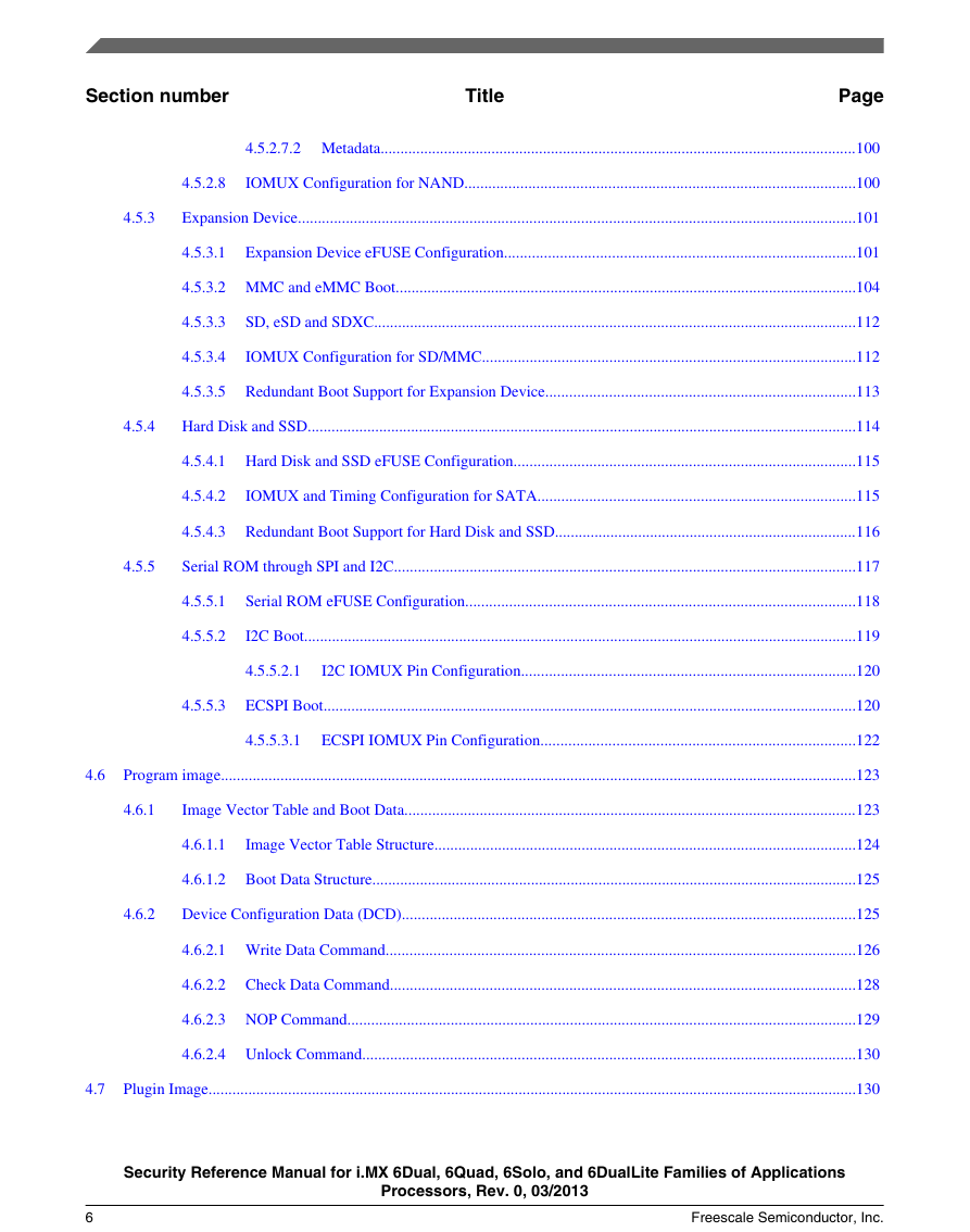
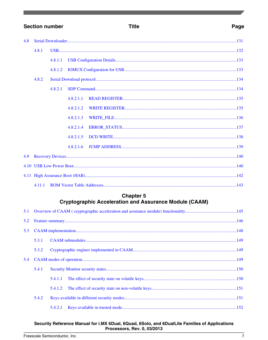
Section number Title Page 4.5.2.7.2 Metadata........................................................................................................................100 4.5.2.8 IOMUX Configuration for NAND..................................................................................................100 4.5.3 Expansion Device............................................................................................................................................101 4.5.3.1 Expansion Device eFUSE Configuration........................................................................................101 4.5.3.2 MMC and eMMC Boot....................................................................................................................104 4.5.3.3 SD, eSD and SDXC.........................................................................................................................112 4.5.3.4 IOMUX Configuration for SD/MMC..............................................................................................112 4.5.3.5 Redundant Boot Support for Expansion Device..............................................................................113 4.5.4 Hard Disk and SSD..........................................................................................................................................114 4.5.4.1 Hard Disk and SSD eFUSE Configuration......................................................................................115 4.5.4.2 IOMUX and Timing Configuration for SATA................................................................................115 4.5.4.3 Redundant Boot Support for Hard Disk and SSD............................................................................116 4.5.5 Serial ROM through SPI and I2C....................................................................................................................117 4.5.5.1 Serial ROM eFUSE Configuration..................................................................................................118 4.5.5.2 I2C Boot...........................................................................................................................................119 4.5.5.2.1 I2C IOMUX Pin Configuration....................................................................................120 4.5.5.3 ECSPI Boot......................................................................................................................................120 4.5.5.3.1 ECSPI IOMUX Pin Configuration...............................................................................122 4.6 Program image................................................................................................................................................................123 4.6.1 Image Vector Table and Boot Data..................................................................................................................123 4.6.1.1 Image Vector Table Structure..........................................................................................................124 4.6.1.2 Boot Data Structure..........................................................................................................................125 4.6.2 Device Configuration Data (DCD)..................................................................................................................125 4.6.2.1 Write Data Command......................................................................................................................126 4.6.2.2 Check Data Command.....................................................................................................................128 4.6.2.3 NOP Command................................................................................................................................129 4.6.2.4 Unlock Command............................................................................................................................130 4.7 Plugin Image...................................................................................................................................................................130 Security Reference Manual for i.MX 6Dual, 6Quad, 6Solo, and 6DualLite Families of Applications Processors, Rev. 0, 03/2013 6 Freescale Semiconductor, Inc.
Section number Title Page 4.8 Serial Downloader..........................................................................................................................................................131 4.8.1 USB..................................................................................................................................................................132 4.8.1.1 USB Configuration Details..............................................................................................................133 4.8.1.2 IOMUX Configuration for USB......................................................................................................133 4.8.2 Serial Download protocol................................................................................................................................134 4.8.2.1 SDP Command.................................................................................................................................134 4.8.2.1.1 READ REGISTER........................................................................................................135 4.8.2.1.2 WRITE REGISTER......................................................................................................135 4.8.2.1.3 WRITE_FILE...............................................................................................................136 4.8.2.1.4 ERROR_STATUS........................................................................................................137 4.8.2.1.5 DCD WRITE................................................................................................................138 4.8.2.1.6 JUMP ADDRESS.........................................................................................................139 4.9 Recovery Devices...........................................................................................................................................................140 4.10 USB Low Power Boot....................................................................................................................................................140 4.11 High Assurance Boot (HAB)..........................................................................................................................................142 4.11.1 ROM Vector Table Addresses.........................................................................................................................143 Cryptographic Acceleration and Assurance Module (CAAM) Chapter 5 5.1 Overview of CAAM ( cryptographic acceleration and assurance module) functionality..............................................145 5.2 Feature summary.............................................................................................................................................................146 5.3 CAAM implementation..................................................................................................................................................148 5.3.1 CAAM submodules..........................................................................................................................................149 5.3.2 Cryptographic engines implemented in CAAM..............................................................................................149 5.4 CAAM modes of operation.............................................................................................................................................149 5.4.1 Security Monitor security states.......................................................................................................................150 5.4.1.1 The effect of security state on volatile keys.....................................................................................150 5.4.1.2 The effect of security state on non-volatile keys.............................................................................151 5.4.2 Keys available in different security modes......................................................................................................151 5.4.2.1 Keys available in trusted mode........................................................................................................152 Security Reference Manual for i.MX 6Dual, 6Quad, 6Solo, and 6DualLite Families of Applications Processors, Rev. 0, 03/2013 Freescale Semiconductor, Inc. 7
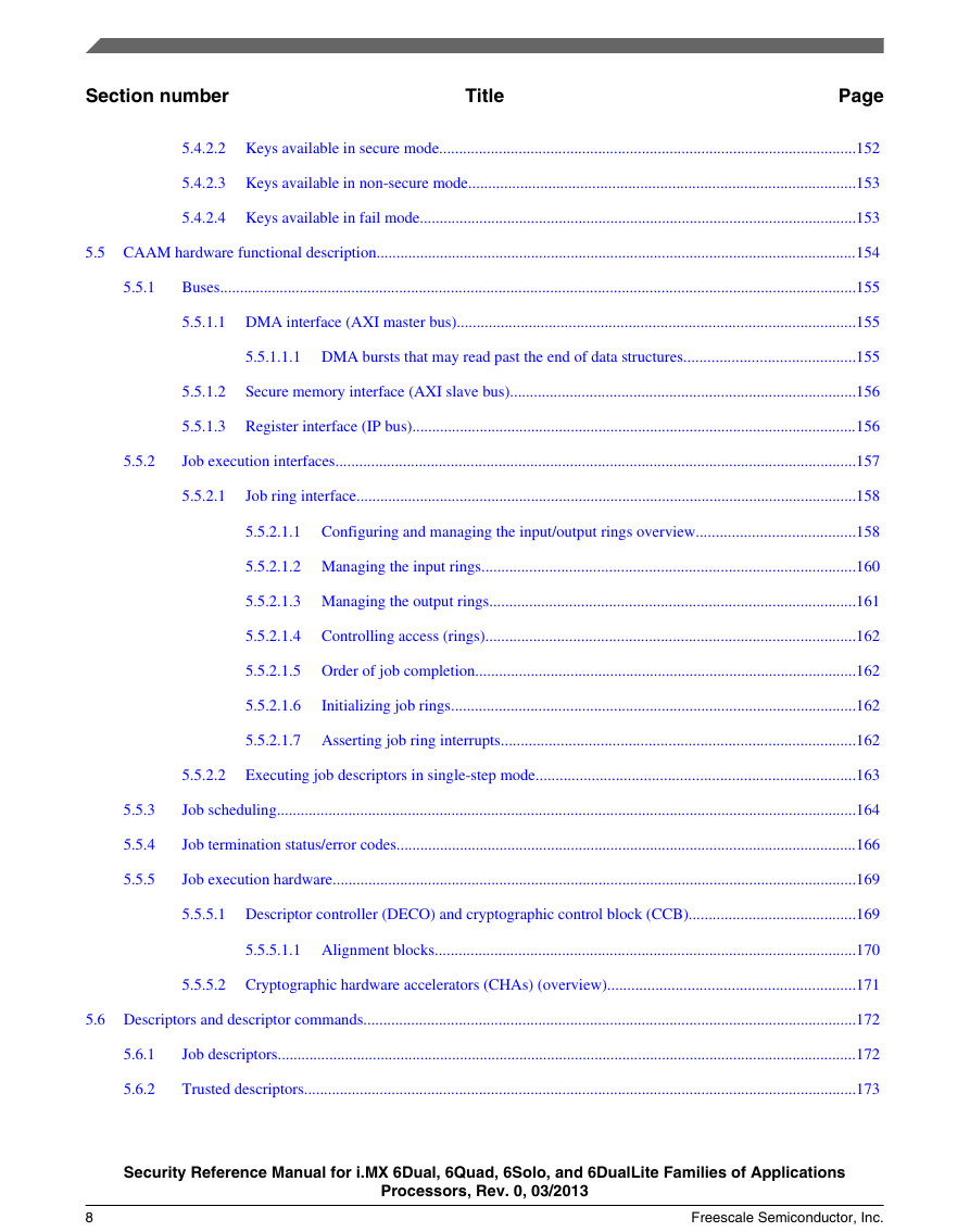
Section number Title Page 5.4.2.2 Keys available in secure mode.........................................................................................................152 5.4.2.3 Keys available in non-secure mode.................................................................................................153 5.4.2.4 Keys available in fail mode..............................................................................................................153 5.5 CAAM hardware functional description.........................................................................................................................154 5.5.1 Buses................................................................................................................................................................155 5.5.1.1 DMA interface (AXI master bus)....................................................................................................155 5.5.1.1.1 DMA bursts that may read past the end of data structures...........................................155 5.5.1.2 Secure memory interface (AXI slave bus).......................................................................................156 5.5.1.3 Register interface (IP bus)................................................................................................................156 5.5.2 Job execution interfaces...................................................................................................................................157 5.5.2.1 Job ring interface..............................................................................................................................158 5.5.2.1.1 Configuring and managing the input/output rings overview........................................158 5.5.2.1.2 Managing the input rings..............................................................................................160 5.5.2.1.3 Managing the output rings............................................................................................161 5.5.2.1.4 Controlling access (rings).............................................................................................162 5.5.2.1.5 Order of job completion................................................................................................162 5.5.2.1.6 Initializing job rings......................................................................................................162 5.5.2.1.7 Asserting job ring interrupts.........................................................................................162 5.5.2.2 Executing job descriptors in single-step mode................................................................................163 5.5.3 Job scheduling..................................................................................................................................................164 5.5.4 Job termination status/error codes....................................................................................................................166 5.5.5 Job execution hardware....................................................................................................................................169 5.5.5.1 Descriptor controller (DECO) and cryptographic control block (CCB)..........................................169 5.5.5.1.1 Alignment blocks..........................................................................................................170 5.5.5.2 Cryptographic hardware accelerators (CHAs) (overview)..............................................................171 5.6 Descriptors and descriptor commands............................................................................................................................172 5.6.1 Job descriptors..................................................................................................................................................172 5.6.2 Trusted descriptors...........................................................................................................................................173 Security Reference Manual for i.MX 6Dual, 6Quad, 6Solo, and 6DualLite Families of Applications Processors, Rev. 0, 03/2013 8 Freescale Semiconductor, Inc.
分享到:
收藏