logo资料库

IMX305LQR-C_Data_Sheet(E)_E16907B96.pdf

第1页 / 共93页
第2页 / 共93页
第3页 / 共93页
第4页 / 共93页
第5页 / 共93页
第6页 / 共93页
第7页 / 共93页
第8页 / 共93页
资料共93页,剩余部分请下载后查看
Description
Features
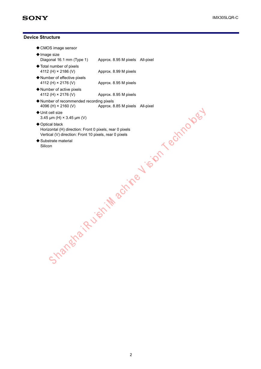
Device Structure
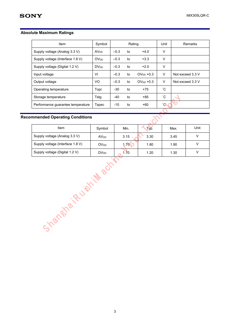
Absolute Maximum Ratings
Recommended Operating Conditions
USE RESTRICTION NOTICE
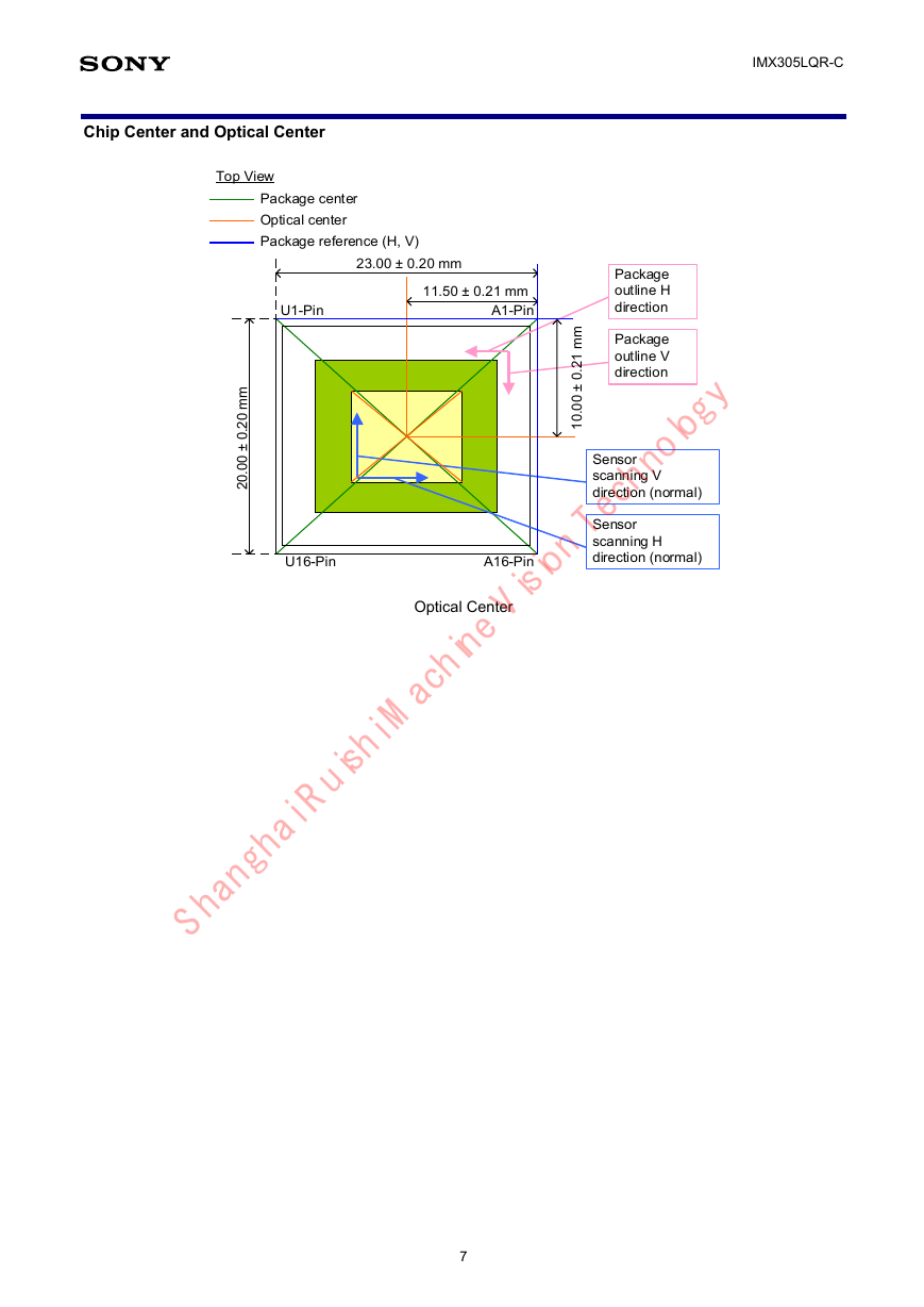
Chip Center and Optical Center
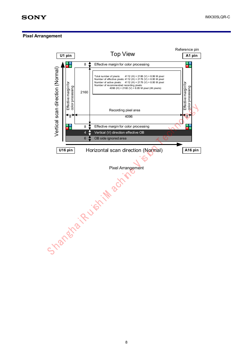
Pixel Arrangement
Block Diagram and Pin Configuration
Pin Description
Electrical Characteristics
DC Characteristics
Power Consumption
AC Characteristics
Master Clock (INCK) Waveform Diagram
XVS / XHS Input Characteristics in Slave Mode (XMASTER = High)
Serial Communication
DLCKPy / DLCKMy, DLOPxy / DLOMxy
I/O Equivalent Circuit Diagram
Spectral Sensitivity Characteristics
Image Sensor Characteristics
Zone Definition of Video Signal Shading
Image Sensor Characteristics Measurement Method
Measurement Conditions
Color Coding of Physical Pixel Array
Definition of standard imaging conditions
Measurement Method
Setting Registers Using Serial Communication
Description of Setting Registers (4-wire)
Register Communication Timing (4-wire)
Register Write and Read (4-wire)
Description of Setting Registers (I2C)
Register Communication Timing (I2C)
I2C Communication Protocol
I2C Serial Communication Read/Write Operation
Single Read from Random Location
Single Read from Current Location
Sequential Read Starting from Random Location
Sequential Read Starting from Current Location
Single Write to Random Location
Sequential Write Starting from Random Location
Register Map
Chip ID = 02 (Write: Chip ID = 02h, Read: Chip ID = 82h, I2C: 30**h)
Chip ID = 03 (Write: Chip ID = 03h, Read: Chip ID = 83h, I2C: 31**h)
Chip ID = 04 (Write: Chip ID = 04h, Read: Chip ID = 84h, I2C: 32**h)
Chip ID = 05 (Write: Chip ID = 05h, Read: Chip ID = 85h, I2C: 33**h)
Chip ID = 06 (Write: Chip ID = 06h, Read: Chip ID = 86h, I2C: 34**h)
Chip ID = 07 (Write: Chip ID = 07h, Read: Chip ID = 87h, I2C: 35**h)
Chip ID = 08 (Write: Chip ID = 08h, Read: Chip ID = 88h, I2C: 36**h)
Chip ID = 09 (Write: Chip ID = 09h, Read: Chip ID = 89h, I2C: 37**h)
Chip ID = 0A (Write: Chip ID = 0Ah, Read: Chip ID = 8Ah, I2C: 38**h)
Chip ID = 0B (Write: Chip ID = 0Bh, Read: Chip ID = 8Bh, I2C: 39**h)
Chip ID = 0C (Write: Chip ID = 0Ch, Read: Chip ID = 8Ch, I2C: 3A**h)
Chip ID = 0D (Write: Chip ID = 0Dh, Read: Chip ID = 8Dh, I2C: 3B**h)
Chip ID = 0E (Write: Chip ID = 0Eh, Read: Chip ID = 8Eh, I2C: 3C**h)
Chip ID = 0F (Write: Chip ID = 0Fh, Read: Chip ID = 8Fh, I2C: 3D**h)
Chip ID = 10 (Write: Chip ID = 10h, Read: Chip ID = 90h, I2C: 3E**h)
Chip ID = 11 (Write: Chip ID = 11h, Read: Chip ID = 91h, I2C: 3F**h)
Chip ID = 12 (Write: Chip ID = 12h, Read: Chip ID = 92h, I2C: 40**h)
Readout Drive Modes
Sync code
List of Sync Code
Sync Code Output Timing
Image Data Output Format
All-pixel scan
ROI mode
Vertical / Horizontal 1/2 Subsampling mode
4K2K Movie mode
Description of Various Function
Standby mode
Slave Mode and Master Mode
Gain Adjustment Function
Black Level Adjustment Function
Horizontal / Vertical Normal Operation and Inverted Operation
Shutter and Integration Time Settings
Global Shutter (Normal Mode) Operation
Pulse Output Function
Signal Output
Output Pin Settings
Output Pin Bit Width
Output Signal Range
Register Hold Setting
Mode Transition
Other Function
Extension Function
Power-on and Power-off Sequence
Power-on sequence
Power-off Sequence
Sensor Setting Flow
Setting Flow in Sensor Slave Mode
Setting Flow in Sensor Master Mode
Peripheral Circuit
Analog Power Pins
Digital Power Pins
Analog Other Pins
Digital I/O Pins
Output pins
Spot Pixel Specifications
Sport Pixel Zone Definition
Notice on White Pixels Specifications
Measurement Method for Spot Pixels
Spot Pixel Pattern Specification
Marking
Notes On Handling
Package Outline
List of Trademark Logos and Definition Statements
Revision History
Revision History
Diagonal 16.1 mm (Type 1 CMOS solid-state Image Sensor with Square Pixel for Color Cameras IMX305LQR-C Description The IMX305LQR-C is a diagonal 16.1 mm (Type 1) CMOS active pixel type solid-state image sensor with a square pixel array and 8.95 M effective pixels. This chip features a global shutter with variable charge-integration time. This chip operates with analog 3.3 V, digital 1.2 V, and interface 1.8 V triple power supply, and has low power consumption. High sensitivity, low dark current and low PLS characteristics are achieved. (Applications: FA cameras, ITS cameras) ◆ Number of recommended recording pixels: 4096 (H) × 2160 (V) approx. 8.85 M pixels ◆ CMOS active pixel type dots ◆ Built-in timing adjustment circuit, H/V driver and serial communication circuit ◆ Global shutter function ◆ Input frequency Shanghai Ruishi M achine Vision Technology Readout mode All-pixel scan mode Vertical / Horizontal 1 / 2 Subsampling mode ROI mode Vertical / Horizontal‐Normal / Inverted readout mode 0 dB to 24 dB: Analog Gain (0.1 dB step) 24.1 dB to 48 dB: Analog Gain: 24 dB + Digital Gain: 0.1 dB to 24 dB (0.1 dB step) ◆ Readout rate Maximum frame rate in All-pixel scan mode: 12 bit 63.7 frame/s ◆ Variable-speed shutter function (resolution 1 H units) ◆ 12-bit A/D converter ◆ CDS / PGA function ◆ I/O interface Low voltage LVDS (150 mVp-p) serial (4 ch / 8 ch / 16 ch switching) DDR output ◆ Recommended lens F number: 2.8 or more (Close side) ◆ Recommended exit pupil distance: –100 mm to –∞ Features 37.125 MHz / 74.25 MHz / 54 MHz Sony Semiconductor Solutions Corporation reserves the right to change products and specifications without prior notice. This information does not convey any license by any implication or otherwise under any patents or other right. Application circuits shown, if any, are typical examples illustrating the operation of the devices. Sony Semiconductor Solutions Corporation cannot assume responsibility for any problems arising out of the use of these circuits. 1 E16907B96
IMX305LQR-C Device Structure ◆ CMOS image sensor ◆ Image size Diagonal 16.1 mm (Type 1) ◆ Total number of pixels 4112 (H) × 2186 (V) ◆ Number of effective pixels 4112 (H) × 2176 (V) ◆ Number of active pixels 4112 (H) × 2176 (V) Approx. 8.95 M pixels All-pixel Approx. 8.99 M pixels Approx. 8.95 M pixels Approx. 8.95 M pixels ◆ Number of recommended recording pixels 4096 (H) × 2160 (V) ◆ Unit cell size 3.45 µm (H) × 3.45 µm (V) ◆ Optical black ◆ Substrate material Silicon Horizontal (H) direction: Front 0 pixels, rear 0 pixels Vertical (V) direction: Front 10 pixels, rear 0 pixels Approx. 8.85 M pixels All-pixel Shanghai Ruishi M achine Vision Technology 2
Absolute Maximum Ratings IMX305LQR-C Item Symbol Rating Unit Remarks Supply voltage (Analog 3.3 V) Supply voltage (Interface 1.8 V) Supply voltage (Digital 1.2 V) Input voltage Output voltage AVDD OVDD DVDD VI VO –0.3 –0.3 –0.3 –0.3 –0.3 to to to to to +4.0 +3.3 +2.0 OVDD +0.3 OVDD +0.3 V V V V V Not exceed 3.3 V Not exceed 3.3 V Operating temperature Storage temperature Performance guarantee temperature Tspec Recommended Operating Conditions Supply voltage (Analog 3.3 V) Supply voltage (Interface 1.8 V) Supply voltage (Digital 1.2 V) +75 +85 +60 ˚C ˚C ˚C Topr Tstg -30 -40 -10 to to to Min. Item Typ. 1.80 1.70 3.45 3.30 3.15 Max. AVDD DVDD OVDD Symbol Shanghai Ruishi M achine Vision Technology 1.90 1.10 1.20 1.30 Unit V V V 3
USE RESTRICTION NOTICE IMX305LQR-C This USE RESTRICTION NOTICE ("Notice") is for customers who are considering or currently using the image sensor products ("Products") set forth in this specifications book. Sony Semiconductor Solutions Corporation ("SSS") may, at any time, modify this Notice which will be available to you in the latest specifications book for the Products. You should abide by the latest version of this Notice. If a SSS subsidiary or distributor has its own use restriction notice on the Products, such a use restriction notice will additionally apply between you and the subsidiary or distributor. You should consult a sales representative of the subsidiary or distributor of SSS on such a use restriction notice when you consider using the Products. Use Restrictions  The Products are intended for incorporation into such general electronic equipment as office products, communication products, measurement products, and home electronics products in accordance with the terms and conditions set forth in this specifications book and otherwise notified by SSS from time to time.  You should not use the Products for critical applications which may pose a life- or injury-threatening risk or are highly likely to cause significant property damage in the event of failure of the Products. You should consult your sales representative beforehand when you consider using the Products for such critical applications. In addition, you should not use the Products in weapon or military equipment.  SSS disclaims and does not assume any liability and damages arising out of misuse, improper use, modification, use of the Products for the above-mentioned critical applications, weapon and military equipment, or any deviation from the requirements set forth in this specifications book. Design for Safety  SSS is making continuous efforts to further improve the quality and reliability of the Products; however, failure of a certain percentage of the Products is inevitable. Therefore, you should take sufficient care to ensure the safe design of your products such as component redundancy, anti-conflagration features, and features to prevent mis-operation in order to avoid accidents resulting in injury or death, fire or other social damage as a result of such failure. Shanghai Ruishi M achine Vision Technology No License Implied  The technical information shown in this specifications book is for your reference purposes only. The availability of this specifications book shall not be construed as giving any indication that SSS and its licensors will license any intellectual property rights in such information by any implication or otherwise. SSS will not assume responsibility for any problems in connection with your use of such information or for any infringement of third-party rights due to the same. It is therefore your sole legal and financial responsibility to resolve any such problems and infringement. Governing Law  This Notice shall be governed by and construed in accordance with the laws of Japan, without reference to principles of conflict of laws or choice of laws. All controversies and disputes arising out of or relating to this Notice shall be submitted to the exclusive jurisdiction of the Tokyo District Court in Japan as the court of first instance. Export Control  If the Products are controlled items under the export control laws or regulations of various countries, approval may be required for the export of the Products under the said laws or regulations. You should be responsible for compliance with the said laws or regulations. Other Applicable Terms and Conditions  The terms and conditions in the SSS additional specifications, which will be made available to you when you order the Products, shall also be applicable to your use of the Products as well as to this specifications book. You should review those terms and conditions when you consider purchasing and/or using the Products. General-0.0.9 4
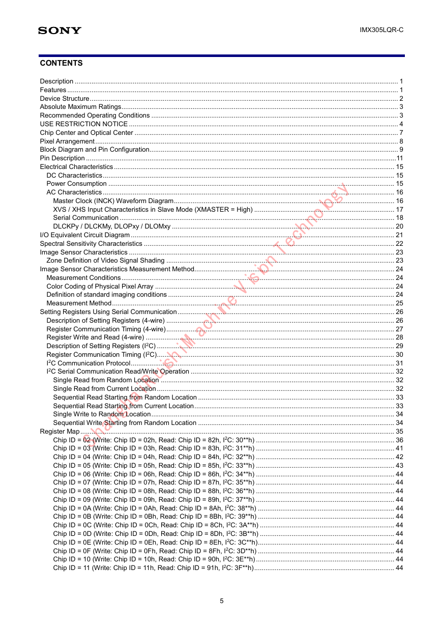
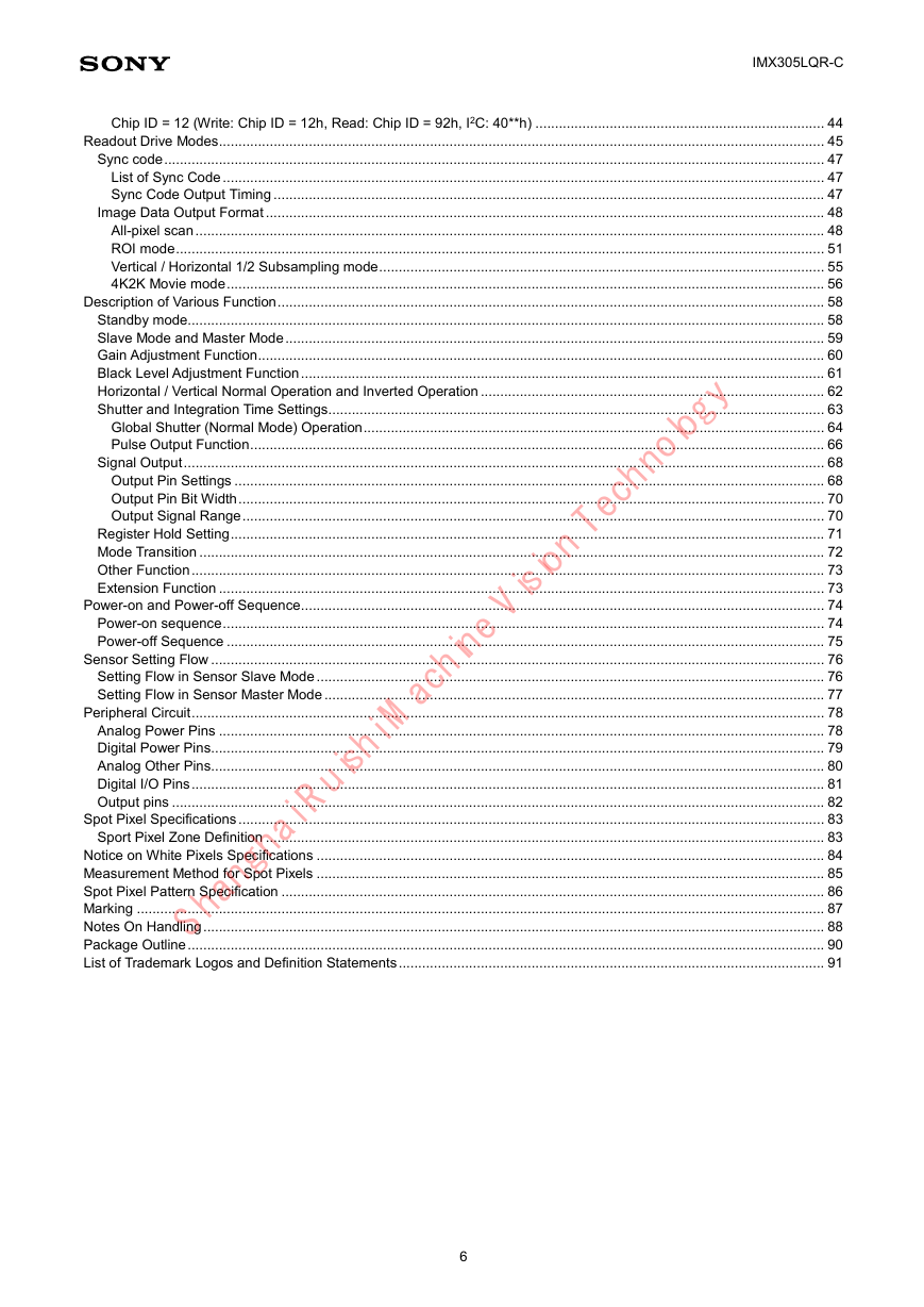
CONTENTS IMX305LQR-C Shanghai Ruishi M achine Vision Technology Description ............................................................................................................................................................................. 1 Features ................................................................................................................................................................................. 1 Device Structure ..................................................................................................................................................................... 2 Absolute Maximum Ratings .................................................................................................................................................... 3 Recommended Operating Conditions .................................................................................................................................... 3 USE RESTRICTION NOTICE ................................................................................................................................................ 4 Chip Center and Optical Center ............................................................................................................................................. 7 Pixel Arrangement .................................................................................................................................................................. 8 Block Diagram and Pin Configuration ..................................................................................................................................... 9 Pin Description ...................................................................................................................................................................... 11 Electrical Characteristics ...................................................................................................................................................... 15 DC Characteristics ............................................................................................................................................................ 15 Power Consumption ......................................................................................................................................................... 15 AC Characteristics ............................................................................................................................................................ 16 Master Clock (INCK) Waveform Diagram ...................................................................................................................... 16 XVS / XHS Input Characteristics in Slave Mode (XMASTER = High) ........................................................................... 17 Serial Communication ................................................................................................................................................... 18 DLCKPy / DLCKMy, DLOPxy / DLOMxy ....................................................................................................................... 20 I/O Equivalent Circuit Diagram ............................................................................................................................................. 21 Spectral Sensitivity Characteristics ...................................................................................................................................... 22 Image Sensor Characteristics .............................................................................................................................................. 23 Zone Definition of Video Signal Shading .......................................................................................................................... 23 Image Sensor Characteristics Measurement Method........................................................................................................... 24 Measurement Conditions .................................................................................................................................................. 24 Color Coding of Physical Pixel Array ................................................................................................................................ 24 Definition of standard imaging conditions ......................................................................................................................... 24 Measurement Method ....................................................................................................................................................... 25 Setting Registers Using Serial Communication .................................................................................................................... 26 Description of Setting Registers (4-wire) .......................................................................................................................... 26 Register Communication Timing (4-wire) .......................................................................................................................... 27 Register Write and Read (4-wire) ..................................................................................................................................... 28 Description of Setting Registers (I2C) ............................................................................................................................... 29 Register Communication Timing (I2C) ............................................................................................................................... 30 I2C Communication Protocol ............................................................................................................................................. 31 I2C Serial Communication Read/Write Operation ............................................................................................................. 32 Single Read from Random Location ............................................................................................................................. 32 Single Read from Current Location ............................................................................................................................... 32 Sequential Read Starting from Random Location ......................................................................................................... 33 Sequential Read Starting from Current Location ........................................................................................................... 33 Single Write to Random Location .................................................................................................................................. 34 Sequential Write Starting from Random Location ......................................................................................................... 34 Register Map ........................................................................................................................................................................ 35 Chip ID = 02 (Write: Chip ID = 02h, Read: Chip ID = 82h, I2C: 30**h) .......................................................................... 36 Chip ID = 03 (Write: Chip ID = 03h, Read: Chip ID = 83h, I2C: 31**h) .......................................................................... 41 Chip ID = 04 (Write: Chip ID = 04h, Read: Chip ID = 84h, I2C: 32**h) .......................................................................... 42 Chip ID = 05 (Write: Chip ID = 05h, Read: Chip ID = 85h, I2C: 33**h) .......................................................................... 43 Chip ID = 06 (Write: Chip ID = 06h, Read: Chip ID = 86h, I2C: 34**h) .......................................................................... 44 Chip ID = 07 (Write: Chip ID = 07h, Read: Chip ID = 87h, I2C: 35**h) .......................................................................... 44 Chip ID = 08 (Write: Chip ID = 08h, Read: Chip ID = 88h, I2C: 36**h) .......................................................................... 44 Chip ID = 09 (Write: Chip ID = 09h, Read: Chip ID = 89h, I2C: 37**h) .......................................................................... 44 Chip ID = 0A (Write: Chip ID = 0Ah, Read: Chip ID = 8Ah, I2C: 38**h) ......................................................................... 44 Chip ID = 0B (Write: Chip ID = 0Bh, Read: Chip ID = 8Bh, I2C: 39**h) ......................................................................... 44 Chip ID = 0C (Write: Chip ID = 0Ch, Read: Chip ID = 8Ch, I2C: 3A**h) ........................................................................ 44 Chip ID = 0D (Write: Chip ID = 0Dh, Read: Chip ID = 8Dh, I2C: 3B**h) ........................................................................ 44 Chip ID = 0E (Write: Chip ID = 0Eh, Read: Chip ID = 8Eh, I2C: 3C**h) ......................................................................... 44 Chip ID = 0F (Write: Chip ID = 0Fh, Read: Chip ID = 8Fh, I2C: 3D**h) ......................................................................... 44 Chip ID = 10 (Write: Chip ID = 10h, Read: Chip ID = 90h, I2C: 3E**h) .......................................................................... 44 Chip ID = 11 (Write: Chip ID = 11h, Read: Chip ID = 91h, I2C: 3F**h) ........................................................................... 44 5
IMX305LQR-C Chip ID = 12 (Write: Chip ID = 12h, Read: Chip ID = 92h, I2C: 40**h) .......................................................................... 44 Readout Drive Modes ........................................................................................................................................................... 45 Sync code ......................................................................................................................................................................... 47 List of Sync Code .......................................................................................................................................................... 47 Sync Code Output Timing ............................................................................................................................................. 47 Image Data Output Format ............................................................................................................................................... 48 All-pixel scan ................................................................................................................................................................. 48 ROI mode ...................................................................................................................................................................... 51 Vertical / Horizontal 1/2 Subsampling mode .................................................................................................................. 55 4K2K Movie mode ......................................................................................................................................................... 56 Description of Various Function ............................................................................................................................................ 58 Standby mode................................................................................................................................................................... 58 Slave Mode and Master Mode .......................................................................................................................................... 59 Gain Adjustment Function ................................................................................................................................................. 60 Black Level Adjustment Function ...................................................................................................................................... 61 Horizontal / Vertical Normal Operation and Inverted Operation ........................................................................................ 62 Shutter and Integration Time Settings ............................................................................................................................... 63 Global Shutter (Normal Mode) Operation ...................................................................................................................... 64 Pulse Output Function ................................................................................................................................................... 66 Signal Output .................................................................................................................................................................... 68 Output Pin Settings ....................................................................................................................................................... 68 Output Pin Bit Width ...................................................................................................................................................... 70 Output Signal Range ..................................................................................................................................................... 70 Register Hold Setting ........................................................................................................................................................ 71 Mode Transition ................................................................................................................................................................ 72 Other Function .................................................................................................................................................................. 73 Extension Function ........................................................................................................................................................... 73 Power-on and Power-off Sequence ...................................................................................................................................... 74 Power-on sequence .......................................................................................................................................................... 74 Power-off Sequence ......................................................................................................................................................... 75 Sensor Setting Flow ............................................................................................................................................................. 76 Setting Flow in Sensor Slave Mode .................................................................................................................................. 76 Setting Flow in Sensor Master Mode ................................................................................................................................ 77 Peripheral Circuit .................................................................................................................................................................. 78 Analog Power Pins ........................................................................................................................................................... 78 Digital Power Pins ............................................................................................................................................................. 79 Analog Other Pins ............................................................................................................................................................. 80 Digital I/O Pins .................................................................................................................................................................. 81 Output pins ....................................................................................................................................................................... 82 Spot Pixel Specifications ...................................................................................................................................................... 83 Sport Pixel Zone Definition ............................................................................................................................................... 83 Notice on White Pixels Specifications .................................................................................................................................. 84 Measurement Method for Spot Pixels .................................................................................................................................. 85 Spot Pixel Pattern Specification ........................................................................................................................................... 86 Marking ................................................................................................................................................................................ 87 Notes On Handling ............................................................................................................................................................... 88 Package Outline ................................................................................................................................................................... 90 List of Trademark Logos and Definition Statements ............................................................................................................. 91 Shanghai Ruishi M achine Vision Technology 6
Chip Center and Optical Center IMX305LQR-C Top View Package center Optical center Package reference (H, V) 23.00 ± 0.20 mm U1-Pin 11.50 ± 0.21 mm A1-Pin Package outline H direction m m 1 2 . 0 Package outline V direction 0 m m 0 2 . A16-Pin U16-Pin ± 0 0 0 2 . ± 0 0 0 1 . Optical Center Sensor scanning H direction (normal) Sensor scanning V direction (normal) Shanghai Ruishi M achine Vision Technology 7
IMX305LQR-C U1 pin G G G G R R RR B B B B G G G G Top View 8 Effective margin for color processing Reference pin A1 pin G G G G R R RR B B B B G G G G Total number of pixels: Number of effective pixels: 4112 (H) × 2176 (V) = 8.95 M pixel Number of active pixels: 4112 (H) × 2176 (V) = 8.95 M pixel Number of recommended recording pixels: 4112 (H) × 2186 (V) = 8.99 M pixel  4096 (H) × 2160 (V) = 8.85 M pixel (All pixels) 2160 r o f i n g r a m e v i g n s s e c o r p r o o c l A16 pin 8 8 f f E f f E B B B G G G G G G RR R G G G RR R B B B G G G i t c e i t c e 8 4 6 4096 U16 pin a c i t r e V Recording pixel area Pixel Arrangement Horizontal scan direction (Normal) Effective margin for color processing Vertical (V) direction effective OB OB side ignored area Shanghai Ruishi M achine Vision Technology Pixel Arrangement ) l a m r o N ( n o i t c e r i d n a c s l r o f i n g r a m e v i g n s s e c o r p r o o c l 8
分享到:
收藏