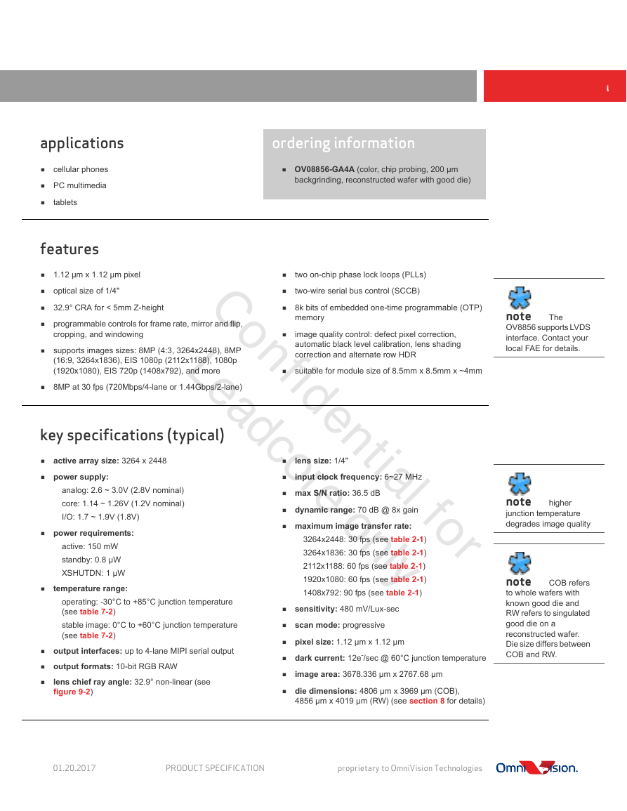
applications
features
key specifications (typical)
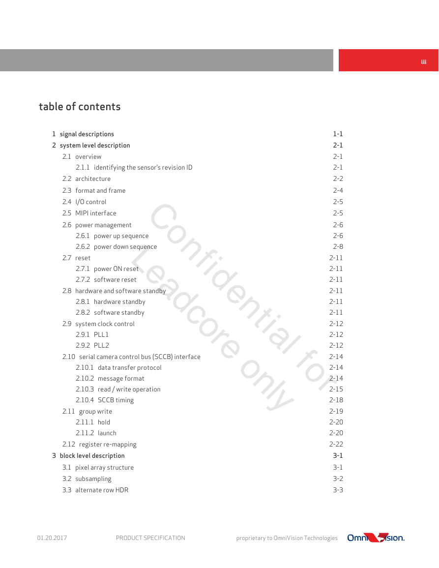
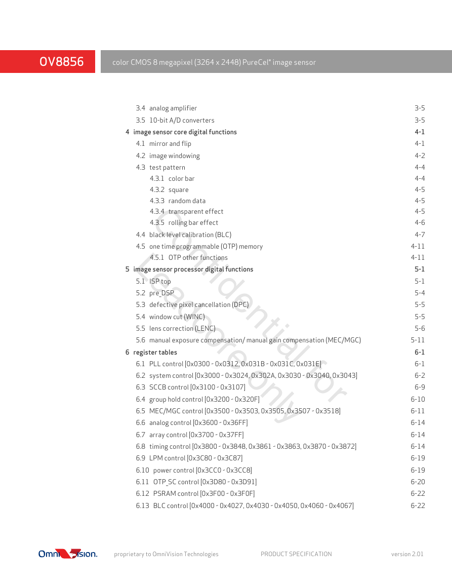
table of contents
list of figures
list of tables
1 signal descriptions
table 1-1 signal descriptions (sheet 1 of 2)
table 1-2 configuration under various conditions (sheet 1 of 2)
figure 1-1 pad diagram
table 1-3 pad symbol and equivalent circuit
2 system level description
2.1 overview
2.1.1 identifying the sensor’s revision ID
2.2 architecture
figure 2-1 OV8856 block diagram
figure 2-2 OV8856 reference schematic
2.3 format and frame
table 2-1 format and frame rate
2.4 I/O control
table 2-2 I/O control registers
2.5 MIPI interface
2.6 power management
2.6.1 power up sequence
table 2-3 power up sequence
table 2-4 power up sequence timing constraints
figure 2-3 power up sequence
2.6.2 power down sequence
table 2-5 power down sequence
table 2-6 power down sequence timing constraints
figure 2-4 software standby sequence
figure 2-5 power down sequence
2.7 reset
2.7.1 power ON reset
2.7.2 software reset
2.8 hardware and software standby
2.8.1 hardware standby
2.8.2 software standby
table 2-7 hardware and standby description
2.9 system clock control
2.9.1 PLL1
2.9.2 PLL2
figure 2-6 clock scheme
table 2-8 PLL registers (sheet 1 of 2)
table 2-9 sample PLL configuration
2.10 serial camera control bus (SCCB) interface
2.10.1 data transfer protocol
2.10.2 message format
figure 2-7 message type
2.10.3 read / write operation
figure 2-8 SCCB single read from random location
figure 2-9 SCCB single read from current location
figure 2-10 SCCB sequential read from random location
figure 2-11 SCCB sequential read from current location
figure 2-12 SCCB single write to random location
figure 2-13 SCCB sequential write to random location
2.10.4 SCCB timing
figure 2-14 SCCB interface timing
table 2-10 SCCB interface timing specifications
2.11 group write
table 2-11 context switching control
2.11.1 hold
2.11.2 launch
2.12 register re-mapping
table 2-12 register re-mapping
3 block level description
3.1 pixel array structure
figure 3-1 sensor array region color filter layout
3.2 subsampling
figure 3-2 example of 2x2 binning
table 3-1 binning-related registers
3.3 alternate row HDR
figure 3-3 alternate row HDR
figure 3-4 HDR output timing
table 3-2 HDR control registers (sheet 1 of 3)
3.4 analog amplifier
3.5 10-bit A/D converters
4 image sensor core digital functions
4.1 mirror and flip
figure 4-1 mirror and flip samples
table 4-1 mirror and flip registers
4.2 image windowing
figure 4-2 image windowing
table 4-2 image windowing control functions
4.3 test pattern
4.3.1 color bar
figure 4-3 color bar types
4.3.2 square
figure 4-4 color, black and white square bars
4.3.3 random data
4.3.4 transparent effect
figure 4-5 transparent effect
4.3.5 rolling bar effect
figure 4-6 rolling bar effect
table 4-3 test pattern registers
4.4 black level calibration (BLC)
table 4-4 BLC control registers (sheet 1 of 4)
4.5 one time programmable (OTP) memory
4.5.1 OTP other functions
table 4-5 OTP control registers (sheet 1 of 2)
5 image sensor processor digital functions
5.1 ISP top
table 5-1 ISP top registers (sheet 1 of 3)
5.2 pre_DSP
table 5-2 pre_DSP registers
5.3 defective pixel cancellation (DPC)
table 5-3 DPC control registers
5.4 window cut (WINC)
table 5-4 WINC control registers
5.5 lens correction (LENC)
figure 5-1 control points of luminance and color channels
figure 5-2 luminance compensation level calculation
table 5-5 LENC control registers (sheet 1 of 4)
5.6 manual exposure compensation/ manual gain compensation (MEC/MGC)
table 5-6 MEC/MGC control registers (sheet 1 of 2)
6 register tables
6.1 PLL control [0x0300 ~ 0x0312, 0x031B ~ 0x031C, 0x031E]
table 6-1 PLL control registers (sheet 1 of 2)
6.2 system control [0x3000 ~ 0x3024, 0x302A, 0x3030 ~ 0x3040, 0x3043]
table 6-2 system control registers (sheet 1 of 7)
6.3 SCCB control [0x3100 ~ 0x3107]
table 6-3 SCCB control registers (sheet 1 of 2)
6.4 group hold control [0x3200 ~ 0x320F]
table 6-4 group hold control registers (sheet 1 of 2)
6.5 MEC/MGC control [0x3500 ~ 0x3503, 0x3505, 0x3507 ~ 0x3518]
table 6-5 MEC/MGC control registers (sheet 1 of 3)
6.6 analog control [0x3600 ~ 0x36FF]
table 6-6 analog control registers
6.7 array control [0x3700 ~ 0x37FF]
table 6-7 array control registers
6.8 timing control [0x3800 ~ 0x3848, 0x3861 ~ 0x3863, 0x3870 ~ 0x3872]
table 6-8 timing control registers (sheet 2 of 5)
6.9 LPM control [0x3C80 ~ 0x3C87]
table 6-9 power saving mode control registers
6.10 power control [0x3CC0 ~ 0x3CC8]
table 6-10 power control registers (sheet 1 of 2)
6.11 OTP_SC control [0x3D80 ~ 0x3D91]
table 6-11 OTP_SC control registers (sheet 1 of 2)
6.12 PSRAM control [0x3F00 ~ 0x3F0F]
table 6-12 PSRAM control registers
6.13 BLC control [0x4000 ~ 0x4027, 0x4030 ~ 0x4050, 0x4060 ~ 0x4067]
table 6-13 BLC control registers (sheet 1 of 5)
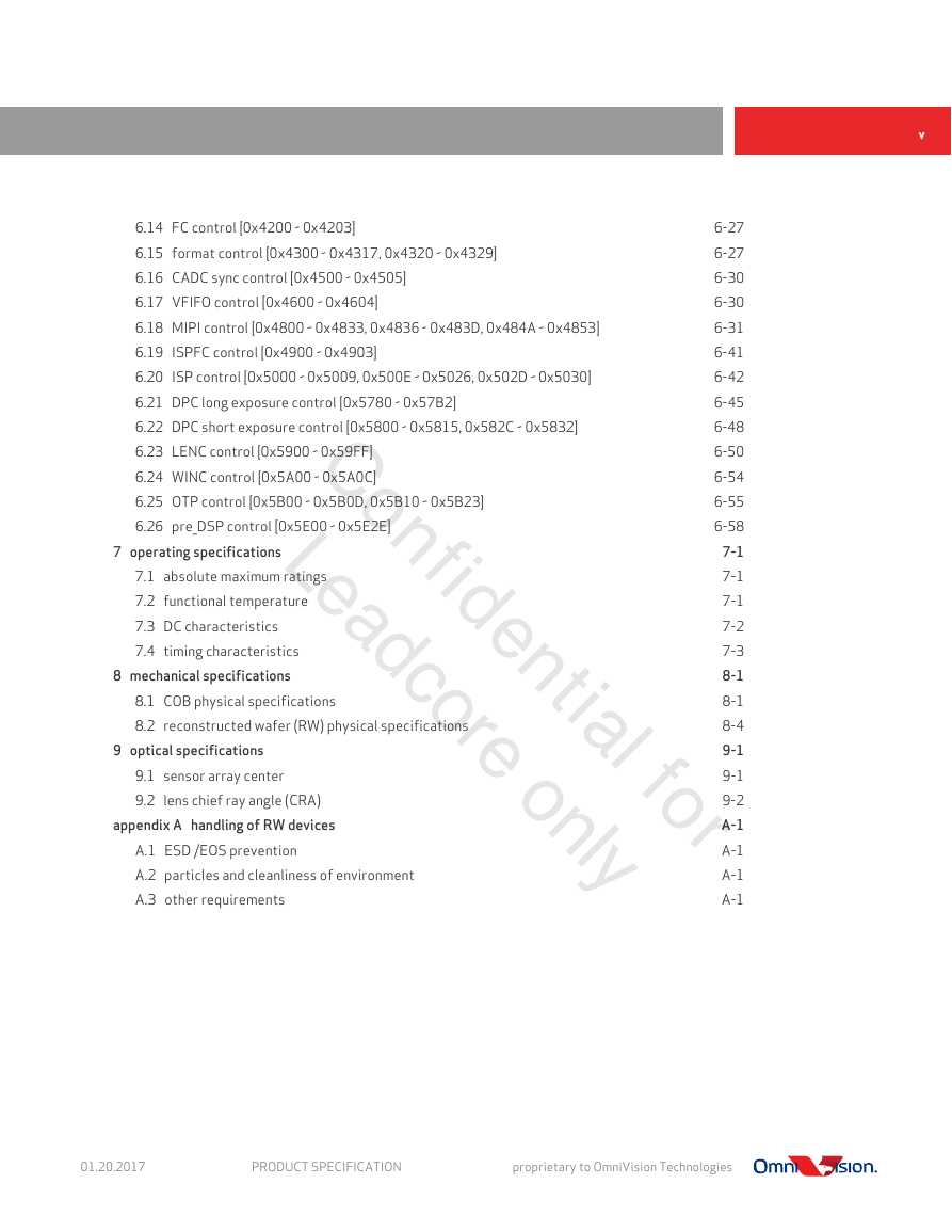
6.14 FC control [0x4200 ~ 0x4203]
table 6-14 FC control registers
6.15 format control [0x4300 ~ 0x4317, 0x4320 ~ 0x4329]
table 6-15 format control registers (sheet 1 of 3)
6.16 CADC sync control [0x4500 ~ 0x4505]
table 6-16 CADC sync control registers
6.17 VFIFO control [0x4600 ~ 0x4604]
table 6-17 VFIFO control registers (sheet 2 of 2)
6.18 MIPI control [0x4800 ~ 0x4833, 0x4836 ~ 0x483D, 0x484A ~ 0x4853]
table 6-18 MIPI control registers (sheet 1 of 11)
6.19 ISPFC control [0x4900 ~ 0x4903]
table 6-19 ISPFC control registers
6.20 ISP control [0x5000 ~ 0x5009, 0x500E ~ 0x5026, 0x502D ~ 0x5030]
table 6-20 ISP control registers (sheet 1 of 3)
6.21 DPC long exposure control [0x5780 ~ 0x57B2]
table 6-21 DPC long exposure control registers (sheet 1 of 3)
6.22 DPC short exposure control [0x5800 ~ 0x5815, 0x582C ~ 0x5832]
table 6-22 DPC short exposure control registers (sheet 1 of 2)
6.23 LENC control [0x5900 ~ 0x59FF]
table 6-23 LENC control registers (sheet 1 of 4)
6.24 WINC control [0x5A00 ~ 0x5A0C]
table 6-24 WINC control registers (sheet 1 of 2)
6.25 OTP control [0x5B00 ~ 0x5B0D, 0x5B10 ~ 0x5B23]
table 6-25 OTP control registers (sheet 1 of 3)
6.26 pre_DSP control [0x5E00 ~ 0x5E2E]
table 6-26 pre_DSP control registers (sheet 1 of 3)
7 operating specifications
7.1 absolute maximum ratings
table 7-1 absolute maximum ratings
7.2 functional temperature
table 7-2 functional temperature
7.3 DC characteristics
table 7-3 DC characteristics (-30°C < TJ < 85°C) (sheet 1 of 2)
7.4 timing characteristics
table 7-4 timing characteristics
8 mechanical specifications
8.1 COB physical specifications
figure 8-1 COB die specifications
table 8-1 pad location coordinates (sheet 1 of 2)
8.2 reconstructed wafer (RW) physical specifications
table 8-2 RW physical dimensions
figure 8-2 OV8856 RW physical diagram
9 optical specifications
9.1 sensor array center
figure 9-1 sensor array center
9.2 lens chief ray angle (CRA)
figure 9-2 chief ray angle (CRA)
table 9-1 CRA versus image height plot
appendix A handling of RW devices
A.1 ESD /EOS prevention
A.2 particles and cleanliness of environment
A.3 other requirements
revision history




 2023年江西萍乡中考道德与法治真题及答案.doc
 2012年重庆南川中考生物真题及答案.doc
 2013年江西师范大学地理学综合及文艺理论基础考研真题.doc
 2020年四川甘孜小升初语文真题及答案I卷.doc
 2020年注册岩土工程师专业基础考试真题及答案.doc
 2023-2024学年福建省厦门市九年级上学期数学月考试题及答案.doc
 2021-2022学年辽宁省沈阳市大东区九年级上学期语文期末试题及答案.doc
 2022-2023学年北京东城区初三第一学期物理期末试卷及答案.doc
 2018上半年江西教师资格初中地理学科知识与教学能力真题及答案.doc
 2012年河北国家公务员申论考试真题及答案-省级.doc
 2020-2021学年江苏省扬州市江都区邵樊片九年级上学期数学第一次质量检测试题及答案.doc
 2022下半年黑龙江教师资格证中学综合素质真题及答案.doc