VK16K33 LED Driver IC
RAM Mapping 16*8 LED Controller Driver with keyscan
General Description
The VK16K33 is a memory mapping and multi-function LED controller driver. The max. Display
segment numbers in the device is 128 patterns (16 segments and 8 commons) with a 13*3 (MAX.) matrix key
scan circuit. The software configuration features of the VK16K33 makes it suitable for multiple LED applications
including LED modules and display subsystems. The VK16K33 is compatible with most microcontrollers and
communicates via a two-line bidirectional I2C -bus.
Features
Operating voltage: 4.5V~5.5V
Integrated RC oscillator
I2C-bus interface
16*8 bits RAM for display data storage
Max. 16 x 8 patterns, 16 segments and 8 commons
R/W address auto increment
Max. 13 x 3 matrix key scanning
16-step dimming circuit
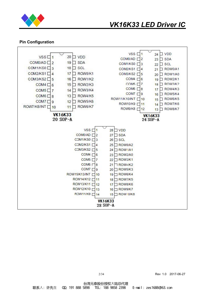
Selection of 20/24/28-pin SOP package types
Application
Industrial control indicators
Digital clocks, thermometers, counters, multimeters
Combo sets
VCR sets
Instrumentation readouts
Other consumer applications
LED Displays
1/34
Rev 1.0 2017-06-27
台湾元泰股份授权大陆总代理 联系人:许先生 QQ:191 888 5898 TEL:188 9858 2398 E-mail:zes1688@163.com�
VK16K33 LED Driver IC
Pin Configuration
2/34
Rev 1.0 2017-06-27
台湾元泰股份授权大陆总代理 联系人:许先生 QQ:191 888 5898 TEL:188 9858 2398 E-mail:zes1688@163.com�
VK16K33 LED Driver IC
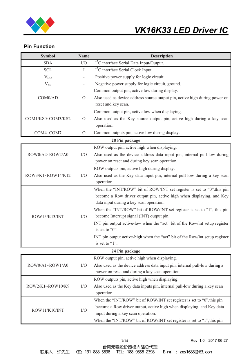
Pin Function
Symbol
SDA
SCL
VDD
VSS
COM0/AD
COM1/KS0~COM3/KS2
COM4~COM7
Name
I/O
I
-
-
O
O
O
Description
I2C interface Serial Data Input/Output.
I2C interface Serial Clock Input.
Positive power supply for logic circuit.
Negative power supply for logic circuit, ground.
Common output pin, active low during display.
Also used as device address source output pin, active high during power on
reset and key scan.
Common output pin, active low when displaying.
Also used as the Key source output pin, active high during a key scan
operation.
Common outputs pin, active low during display.
ROW0/A2~ROW2/A0
I/O
ROW3/K1~ROW14/K12
I/O
ROW15/K13/INT
I/O
ROW0/A1~ROW1/A0
I/O
ROW2/K1~ROW10/K9
I/O
ROW11/K10/INT
I/O
28 Pin package
ROW output pin, active high when displaying.
Also used as the device address data input pin, internal pull-low during
power on reset and during key scan operation.
ROW outputs pin, active high during display.
Also used as the Key data input pin, internal pull-low during a key scan
operation.
When the “INT/ROW” bit of ROW/INT set register is set to “0”,this pin
become a Row driver output pin, active high when displaying, and Key
data input during a key scan operation.
When the “INT/ROW” bit of ROW/INT set register is set to “1”, this pin
become Interrupt signal (INT) output pin.
INT pin output active-low when the “act” bit of the Row/int setup register
is set to “0”.
INT pin output active-high when the “act” bit of the Row/int setup register
is set to “1”.
24 Pin package
ROW output pin, active high when displaying.
Also used as the device address data input pin, internal pull-low during a
power on reset and during a key scan operation.
ROW outputs pin, active high when displaying.
Also used as the Key data inputs pin, internal pull-low during a key scan
operation.
When the “INT/ROW” bit of ROW/INT set register is set to “0”,this pin
become a Row driver output, active high when displaying, and Key data
input during a key scan operation.
When the “INT/ROW” bit of ROW/INT set register is set to “1”,this pin
3/34
Rev 1.0 2017-06-27
台湾元泰股份授权大陆总代理 联系人:许先生 QQ:191 888 5898 TEL:188 9858 2398 E-mail:zes1688@163.com�
VK16K33 LED Driver IC
become an Interrupt signal (INT) output pin.
INT pin output active-low when the “act” bit of the Row/int setup register
is set to “0”.
INT pin output active-high when the “act” bit of the Row/int setup register
is set to “1”.
20 Pin package
ROW output pin, active high when displaying.
Also used as the Key data inputs pin, internal pull-low during a key scan
operation.
When the “INT/ROW” bit of the ROW/INT setup register is set to “0”,this
pin become a Row driver output, active high when displaying, and Key
data input during a key scan operation.
When the “INT/ROW” bit of the ROW/INT set register is set to “1”,this
pin become an Interrupt (INT) signal output pin.
INT pin output active-low when the “act” bit of Row/int setup register is
set to “0”.
INT pin output active-high when the “act” bit of the Row/int setup register
is set to “1”.
ROW0/K1~ROW6/K7
I/O
ROW7/K8 /INT
I/O
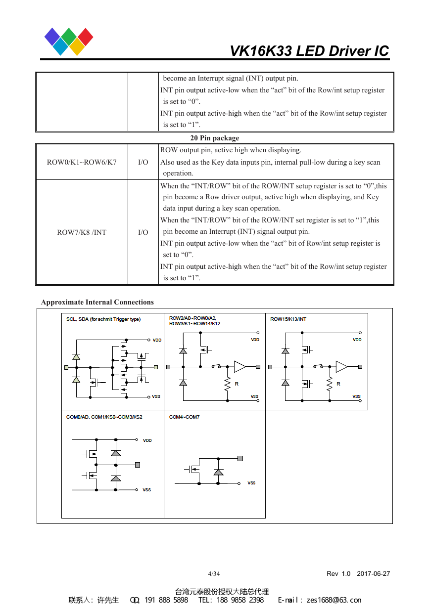
Approximate Internal Connections
4/34
Rev 1.0 2017-06-27
台湾元泰股份授权大陆总代理 联系人:许先生 QQ:191 888 5898 TEL:188 9858 2398 E-mail:zes1688@163.com�
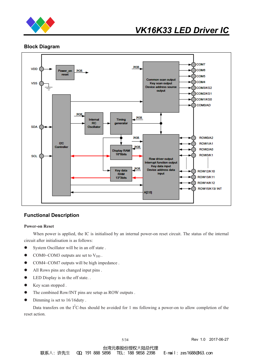
Block Diagram
VK16K33 LED Driver IC
Functional Description
Power-on Reset
When power is applied, the IC is initialised by an internal power-on reset circuit. The status of the internal
circuit after initialisation is as follows:
System Oscillator will be in an off state .
COM0~COM3 outputs are set to VDD .
COM4~COM7 outputs will be high impedance .
All Rows pins are changed input pins .
LED Display is in the off state. .
Key scan stopped .
The combined Row/INT pins are setup as ROW outputs .
Dimming is set to 16/16duty .
Data transfers on the I2C-bus should be avoided for 1 ms following a power-on to allow completion of the
reset action.
5/34
Rev 1.0 2017-06-27
台湾元泰股份授权大陆总代理 联系人:许先生 QQ:191 888 5898 TEL:188 9858 2398 E-mail:zes1688@163.com�
VK16K33 LED Driver IC
Standby Mode
In the standby mode, the VK16K33 can not accept input commands nor write data to the display RAM
except using the system setup command.
If the standby mode is selected with the “S” bit of the system setup register set to “0”, the status of the
standby model is as follows:
System Oscillator will be in the off state .
COM0~COM3 outputs are set to VDD .
COM4~COM7 outputs will be high impedance .
LED Display is in the off state.
Key scan stopped .
All key data and INT flags are cleared until the standby mode is canceled.
If the key matrix is activated (any key) or the “S” bit of the system setup register is set to “1”, the standby
mode will be canceled and will cause the device to wake-up.
If the “INT/ROW” bit of the ROW/INT setup register is set to “0”, all rows pins are changed to input pins.
If the “INT/ROW” bit of the ROW/INT setup register is set to “1”: all rows pins are changed to input pins
except for the INT pin (output).
The INT pin output will remain at a high level when the “act” bit of the ROW/INT setup register is set to
“0”.
The INT pin output remains at a low level when the “act” bit of the ROW/INT setup register is set to “1”.
Wake-up
Wake-up by a key press from any key or by setting the “S” bit of the system setup register to “1”. A key scan
will then be performed.
The System Oscillator restarts for normal operation.
The previous display data output will be updated by Each Mode command set.
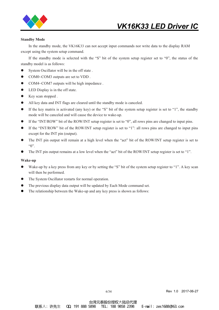
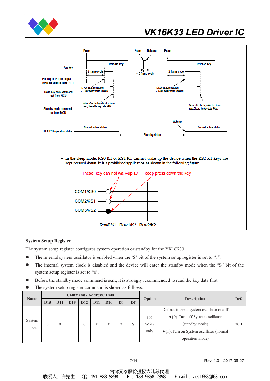
The relationship between the Wake-up and any key press is shown as follows:
6/34
Rev 1.0 2017-06-27
台湾元泰股份授权大陆总代理 联系人:许先生 QQ:191 888 5898 TEL:188 9858 2398 E-mail:zes1688@163.com�
VK16K33 LED Driver IC
System Setup Register
The system setup register configures system operation or standby for the VK16K33
The internal system oscillator is enabled when the ‘S’ bit of the system setup register is set to “1”.
The internal system clock is disabled and the device will enter the standby mode when the “S” bit of the
system setup register is set to “0”.
Before the standby mode command is sent, it is strongly recommended to read the key data first.
The system setup register command is shown as follows:
Command / Address / Data
D15 D14 D13 D12 D11 D10
D9
D8
0
0
1
0
X
X
X
S
Name
System
set
Option
Description
Def.
{S}
Write
only
Defines internal system oscillator on/off
●{0}:Turn off System oscillator
(standby mode)
20H
●{1}:Turn on System oscillator (normal
operation mode)
7/34
Rev 1.0 2017-06-27
台湾元泰股份授权大陆总代理 联系人:许先生 QQ:191 888 5898 TEL:188 9858 2398 E-mail:zes1688@163.com�
VK16K33 LED Driver IC
ROW/INT Set Register
The ROW/INT setup register can be set to either an LED Row output, or an INT logic output.
The INT output is selected when the ROW/INT set register is set to “1”.
The ROW output is selected when the ROW/INT set register is set to “0”.
The INT logic output can be configured as an INT output level controlled by the keys can circuitry and
controlled through the 2-wire interface.
The INT output is active-low when the ‘act’ bit of ROW/INT set register is set to “0”.
The INT output is active-high when the ‘act’ bit of ROW/INT set t register is set to “1”.
The ROW/INT setup register command is shown as follows:
Name
row/int
set
Command / Address / Data
D15 D14 D13 D12 D11 D10
D9
D8
Option
Description
Def.
1
0
1
0
X
X
act
row/
int
{act,row
/int }
Write
only
●Defines INT/ROW output pin select
and INT pin output active level status.
●{X 0}: INT/ROW output pin is set to
ROW driver output.
●{0,1}: INT/ROW output pin is set to
INT output,active low.
●{1,1}: INT/ROW output pin is set to
INT output,active high.
A0H
Display Setup Register
The display setup register configures the LED display on/off and the blinking frequency for the VK16K33.
The LED display is enabled when the ‘D’ bit of the display setup register is set to “1”.
The LED display is disabled when the ‘D’ bit of the display setup register is set to “0”.
In the display disable status, all ROW outputs are hi-impedance and all COM outputs are high-impedance
during the display period.
In the display disable status, all ROWs are changed to an input status and the COM0~COM3 continues
scanning and COM4~COM7 outputs are high-impedance during the keys can period.
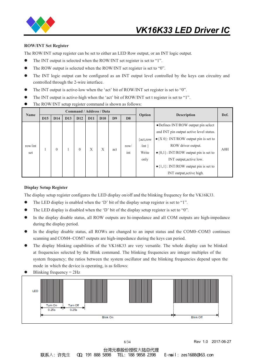
The display blinking capabilities of the VK16K33 are very versatile. The whole display can be blinked
at frequencies selected by the Blink command. The blinking frequencies are integer multiples of the
system frequency; the ratios between the system oscillator and the blinking frequencies depend upon the
mode in which the device is operating, is as follows:
Blinking frequency = 2Hz
8/34
Rev 1.0 2017-06-27
台湾元泰股份授权大陆总代理 联系人:许先生 QQ:191 888 5898 TEL:188 9858 2398 E-mail:zes1688@163.com�



 2023年江西萍乡中考道德与法治真题及答案.doc
 2012年重庆南川中考生物真题及答案.doc
 2013年江西师范大学地理学综合及文艺理论基础考研真题.doc
 2020年四川甘孜小升初语文真题及答案I卷.doc
 2020年注册岩土工程师专业基础考试真题及答案.doc
 2023-2024学年福建省厦门市九年级上学期数学月考试题及答案.doc
 2021-2022学年辽宁省沈阳市大东区九年级上学期语文期末试题及答案.doc
 2022-2023学年北京东城区初三第一学期物理期末试卷及答案.doc
 2018上半年江西教师资格初中地理学科知识与教学能力真题及答案.doc
 2012年河北国家公务员申论考试真题及答案-省级.doc
 2020-2021学年江苏省扬州市江都区邵樊片九年级上学期数学第一次质量检测试题及答案.doc
 2022下半年黑龙江教师资格证中学综合素质真题及答案.doc