AN5346
Application note
STM32G4 ADC use tips and recommendations
Introduction
The STM32G4 Series microcontrollers are designed to support high-end analog applications. These MCUs embed high-
performance analog peripherals (ADCs, DACs, COMPs, OPAMPs, reference voltage) and high-performance digital components
such as their Arm® Cortex®-M4 CPU, mathematical accelerators, DMA, and high-resolution timer among others.
This application note presents specific properties of the embedded ADCs in the STM32G4 Series and an introduction on how to
properly design an application using those specific ADC properties.
This document introduces the specific ADC properties that influence the ADC accuracy of a final application and explains how to
correctly design application hardware and software to improve the ADC accuracy for various application cases.
AN5346 - Rev 2 - October 2019
For further information contact your local STMicroelectronics sales office.
www.st.com
�
AN5346
STM32G4 ADC features
1
STM32G4 ADC features
This document uses as reference the specific STM32G4 ADC features listed in Table 1. This table presents the
basic numeric values used as reference in the following sections.
Features
Number of ADCs
Resolution
Number of input channels
ADC principle
ADC clock frequency
Sampling rate
Sampling time
Supply voltage
Reference voltage
Triggers
Conversion modes
Others
Table 1. ADC features on STM32G4 Series
Values for STM32G4 Series
Up to 5
12 bits (or 10, 8, 6 bits), 16 bits with oversampling
Up to 42
Successive approximation register (SAR)
Up to 60 MHz (up to 52 MHz in multiple-ADC operation case)
Up to 4 Msps (up to 3.46 Msps in multiple-ADC operation case)
2.5 to 640.5 [ADC clock periods]
VDDA = 1.62 V to 3.6 V
On dedicated VREF+ pin(1) (internal or external), VREF+ = 1.62 V to VDDA (see
datasheet)
From external pins or internal peripherals (timers)
Single, continuous, scan-selected channels, discontinuous mode
Offset calibration, analog watchdog, hardware oversampling, offset compensation, gain
compensation, interleaved mode (two ADCs coupled), sampling time controlled by
trigger edges, bulb mode sampling
1.
In the LQFP128-pin packages, two VREF+ pins are available.
For more detailed information on ADC features and characteristics on STM32G4 Series, refer to the
corresponding products datasheet and reference manual (RM0440) available at www.st.com.
The STM32G4 Series microcontrollers are based on the Arm® Cortex®-M4 processor.
Arm is a registered trademark of Arm Limited (or its subsidiaries) in the US and/or elsewhere.
Note:
AN5346 - Rev 2
page 2/15
�
AN5346
Maximum ADC speed
2
2.1
Maximum ADC speed
Successive approximation principle
The ADC in STM32G4 Series is based on the successive approximation register principle. This principle is
depicted in the figure below:
Figure 1. ADC operation based on successive approximation principle
Clock
SAR
EOC
DN-1
DN-2
D2 D1 D0
VREF
DAC
Comparator
-
+
V IN
S/H
The input voltage (VIN) is sampled by the sample-and-hold block (S/H) (as voltage on sampling capacitor) to have
stable voltage during conversion time. This sampled voltage is then compared by the comparator with a known
voltage. This known voltage is provided by the DAC that is supplied by the reference voltage VREF.
The DAC digital input is generated by the successive approximation register (SAR) as a digital word. This digital
word is generated according to the result from the comparator and is based on the successive approximation
principle. The SAR initially generates a word corresponding to a half-voltage range. If the result from the
comparator is zero (meaning that input voltage is less than ½ VREF), then, in the second step, the word
corresponding ¼ VREF is generated by the SAR . In each approximation step, the SAR adds or subtracts 2n
weight according to the current step result from the comparator. After N steps, the SAR generates a final word
that is the ADC digital result. The generated analog voltage is close to the measured voltage (with maximum
½ LSB difference).
Maximum ADC speed in successive approximation
The maximum ADC speed is given for the successive approximation principle by the DAC speed and the
comparator speed (see Figure 1). In each successive approximation clock cycle, the DAC must set the correct
stable analog voltage on its output (with ½ LSB accuracy) and the comparator must provide the result at the end
of each cycle.
For example: If the ADC clock is 60 MHz, then each ADC clock cycle takes 1 / 60 MHz = 16 ns. This 16 ns time
represents the DAC output stabilization time plus the propagation delay of the comparator.
Switched capacitors
The ADC principle in STM32 MCUs is based on successive approximation where the DAC is based on switched-
capacitor network. The capacitor network implementation is technologically acceptable and precise. The
advantage of this solution is that the capacitive network works also as sampling capacitor. So there is no need to
have one more additional sampling capacitor.
The principle of this implementation is explained in section 1. ADC internal principle of the application note How to
get the best ADC accuracy in STM32 microcontrollers (AN2834).
2.2
2.3
AN5346 - Rev 2
page 3/15
�
AN5346
Parasitic components
The figure below shows the basic principle of switched-capacitor SAR ADC principle (for a 10-bit ADC).
Figure 2. Basic schematic of SAR switched-capacitor ADC (10-bit ADC example)
VIN
Sa
S4
C/8
A
S2
C/2
S3
C/4
S1
C
Sb
Note: This is a schematic of an ADC with digital output.
VREF
S5
S6
S7
S8
S9
S10
S11
C/16
C/32
C/64
C/128 C/256
C/512 C/512
PRQ
D
CLK
CLR
ADC data
ADC clk
In this figure, the input voltage (VIN) is connected through sampling switch (Sa) to the whole capacitive network
that works as sampling capacitor (its charging duration defines the sampling time, Sb is closed). The whole
capacitive network is charged to VIN voltage. Then the Sa switches from VIN to VREF and Sb is open. Then the
successive approximation is performed: in each clock cycle, the switches S1 to S11 are rearranged and the
comparator compares the final voltage. During each S1 to S11 switches rearrangement, there is a charge
redistribution between capacitors.
Parasitic components
2.4
In each approximation step, the charge redistribution between capacitors is performed. This charge redistribution
causes current peaks between capacitors and also from VREF voltage (see Figure 2). Those current peaks are
limited by the parasitic components: resistance and inductance between capacitors and VREF/VSSA voltage.
At the end of each approximation cycle (ADC clock frequency), all currents must be close to zero because the
voltage must be stable for comparator comparison. The speed to reach this stable state during charge
redistribution is given by all RLC components. The dominant capacity fraction is the capacity of the capacitors
network, respectively rearranged sampling capacitor into serial-parallel combination during the approximation
(given by configuration of S1 to S11 switches).
The R and L components are parasitic:
•
•
R represents the resistance: dominant is the resistivity of switches S1 to S11 (and on-chip metal paths).
L represents the inductance of all conductive paths: dominant is the longest conductive path from VREF/
VSSA pads to VREF/VSSA pins (bonding wires and on-chip metal paths).
In practice there are attenuated voltage and current oscillations in each approximation step. For correct operation,
the amplitude of voltage oscillations (on comparator, respectively on the capacitor network) must decrease below
1 LSB.
The frequency of oscillations is given by LC components and the attenuation is given by RL components. For
rapid attenuation, the inductance must be kept at a low value: exponential decrease of oscillations is given by the
following formula:
e - R / (2 L) . t (envelope of attenuated oscillations at frequency (2πf)2 = 1 / (LC))
The ADC maximum operating frequency is given by those parasitic RL components.
A large decoupling capacitor must be connected directly between pins VREF+ and VSSA. This capacitor creates
an ideal VREF voltage source (fixed DC voltage without oscillations on this decoupling capacitor).
Note:
AN5346 - Rev 2
page 4/15
�
2.5
2.5.1
2.5.2
2.5.3
AN5346
Application design to reach ADC maximum conversion speed
Application design to reach ADC maximum conversion speed
Decoupling capacitor and PCB design
As mentioned in the previous section, the VREF+ pin must be correctly decoupled.
An appropriate decoupling capacitor must be connected between VREF+ and VSSA pins with a minimum added
inductance. Each 1cm of metal path on PCB adds approximately from 6 to 10 nH of inductance. The decoupling
capacitor must be placed as close as possible to VREF+ and VSSA pins without through hole connections that
may create a loop increasing the inductance.
The placement of the decoupling capacitor must be made on the same layer as VREF+ and VSSA pins. The
decoupling capacitor must have a low ESR and a low inductance (for example: ceramic capacitor).
Package selection
The internal parasitic inductance depends on the chip layout and also on the distance between the VREF+/VSSA
pads on chip and the VREF+/VSSA pins on the package (bonding wire length).
This distance is given by the bonding wires and the pins. The pinout of STM32G4 Series MCUs is designed to
have a minimum internal inductance: VREF+ and VSSA pins are adjacent, creating then a minimum current loop
and minimizing the internal inductance (see the figure below).
Figure 3. Example of VREF+ and VSSA pins location on STM32G4 LQFP48 package
VBAT
PC13
PC14 - OSC32_IN
PC15 - OSC32_OUT
PF0 - OSC_IN
PF1 - OSC_OUT
PG10 - NRST
PA0
PA1
PA2
PA3
PA4
1
2
3
4
5
6
7
8
9
10
11
12
0
T
O
O
B
-
8
B
P
D
D
V
S
S
V
9
B
P
7
B
P
6
B
P
5
B
P
4
B
P
3
B
P
5
1
A
P
4
1
A
P
3
1
A
P
8
4
7
4
6
4
5
4
4
4
3
4
2
4
1
4
0
4
9
3
8
3
7
3
LQFP48
3
1
4
1
5
1
6
1
7
1
8
1
9
1
0
2
1
2
2
2
3
2
4
2
5
A
P
6
A
P
7
A
P
0
B
P
1
B
P
2
B
P
A
S
S
V
+
F
E
R
V
A
D
D
V
0
1
B
P
S
S
V
D
D
V
36
35
34
33
32
31
30
29
28
27
26
25
VDD
VSS
PA12
PA11
PA10
PA9
PA8
PB15
PB14
PB13
PB12
PB11
Even though, some packages offer lower distance between chip pads and package pins. For example, the
internal inductance is larger on LQFP packages than on UFBGA, UFQFPN or WLCSP packages, due to longer
wires from pads to pins.
To decrease even more the inductance on large packages (such as the high-pin count LQFP128) has a VREF+
signal connected by two wires to the two VREF+ pins.
Decrease of ADC clock frequency
If the PCB design is not good enough and if there is an additional external inductance, the oscillations are not
attenuated below 1 LSB at the end of the approximation cycle (equal to ADC clock cycle). In this case the ADC
may produce DNL errors at high ADC clock frequency.
The solution is to decrease the ADC clock frequency with keeping, if possible, the required final data sampling
rate.: slow down each approximation cycle and wait more time for attenuation.
Application example
In this example:
•
The ADC is triggered by a timer at a 2 MHz trigger frequency ( ADC conversion triggered every 500 ns).
AN5346 - Rev 2
page 5/15
�
AN5346
STM32G4 multiple ADCs and parallel operations
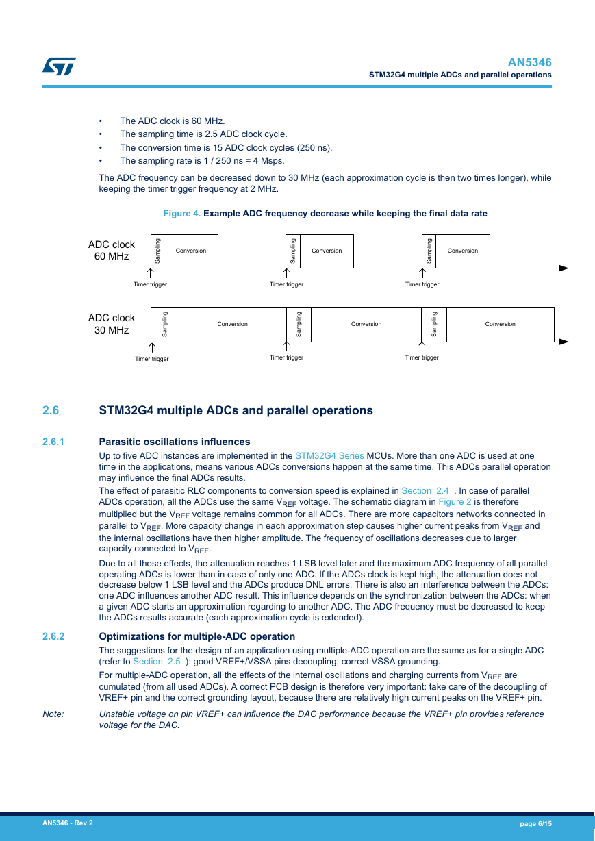
The ADC clock is 60 MHz.
The sampling time is 2.5 ADC clock cycle.
The conversion time is 15 ADC clock cycles (250 ns).
The sampling rate is 1 / 250 ns = 4 Msps.
•
•
•
•
The ADC frequency can be decreased down to 30 MHz (each approximation cycle is then two times longer), while
keeping the timer trigger frequency at 2 MHz.
Figure 4. Example ADC frequency decrease while keeping the final data rate
ADC clock
60 MHz
g
n
i
l
p
m
a
S
Conversion
g
n
i
l
p
m
a
S
Conversion
g
n
i
l
p
m
a
S
Conversion
Timer trigger
Timer trigger
Timer trigger
ADC clock
30 MHz
g
n
i
l
p
m
a
S
Conversion
g
n
i
l
p
m
a
S
Conversion
g
n
i
l
p
m
a
S
Conversion
Timer trigger
Timer trigger
Timer trigger
2.6
2.6.1
2.6.2
Note:
STM32G4 multiple ADCs and parallel operations
Parasitic oscillations influences
Up to five ADC instances are implemented in the STM32G4 Series MCUs. More than one ADC is used at one
time in the applications, means various ADCs conversions happen at the same time. This ADCs parallel operation
may influence the final ADCs results.
The effect of parasitic RLC components to conversion speed is explained in Section 2.4 . In case of parallel
ADCs operation, all the ADCs use the same VREF voltage. The schematic diagram in Figure 2 is therefore
multiplied but the VREF voltage remains common for all ADCs. There are more capacitors networks connected in
parallel to VREF. More capacity change in each approximation step causes higher current peaks from VREF and
the internal oscillations have then higher amplitude. The frequency of oscillations decreases due to larger
capacity connected to VREF.
Due to all those effects, the attenuation reaches 1 LSB level later and the maximum ADC frequency of all parallel
operating ADCs is lower than in case of only one ADC. If the ADCs clock is kept high, the attenuation does not
decrease below 1 LSB level and the ADCs produce DNL errors. There is also an interference between the ADCs:
one ADC influences another ADC result. This influence depends on the synchronization between the ADCs: when
a given ADC starts an approximation regarding to another ADC. The ADC frequency must be decreased to keep
the ADCs results accurate (each approximation cycle is extended).
Optimizations for multiple-ADC operation
The suggestions for the design of an application using multiple-ADC operation are the same as for a single ADC
(refer to Section 2.5 ): good VREF+/VSSA pins decoupling, correct VSSA grounding.
For multiple-ADC operation, all the effects of the internal oscillations and charging currents from VREF are
cumulated (from all used ADCs). A correct PCB design is therefore very important: take care of the decoupling of
VREF+ pin and the correct grounding layout, because there are relatively high current peaks on the VREF+ pin.
Unstable voltage on pin VREF+ can influence the DAC performance because the VREF+ pin provides reference
voltage for the DAC.
AN5346 - Rev 2
page 6/15
�
AN5346
ADC limitation: input channel switch disturbs ongoing conversions
3
3.1
ADC limitation: input channel switch disturbs ongoing conversions
Limitation description
This limitation is described in the errata sheets of the STM32G4 Series MCUs. More details and possible
workarounds are detailed below.
Each ADC has an input multiplexer that performs the selection of a given channel: there are sets of analog
switches between the ADC input and a given pin on the package. The Sa sampling switch (see Figure 2) is
implemented behind the multiplexer. Sa is switched on during sampling time (initiated by the trigger). During the
successive approximation, Sa is open to isolate the capacitors network from the analog input. The multiplexer is
switched to the next programmed channel in the middle of the successive approximation (in case of scan mode).
If the ADC is used in single mode or at the end of the scan sequence, the multiplexer is switched to the internal
channel (Channel 31).
The multiplexer switching from the current channel to the following channel generates some noise that may
influence the successive approximation currently in progress (especially the bit under evaluation in the successive
approximation sequence). This may also impact the DNL error of any ADC currently converting.
The worst case is when various ADCs operates synchronously and their input multiplexers switch to the next
channel at the same clock cycle (usually the case as all ADCs are programmed with the same parameters and
triggered by the same trigger). In this case, the noise is cumulated and the DNL error of the ADC results is
maximal.
Workaround
This workaround is based on disabling the input multiplexer switch during the successive approximation.
The input multiplexer switch is not performed in the following cases:
•
in continuous conversions for the same channel
Continuous conversions are performed on the same channel and the input multiplexer is kept switched on
the given selected channel (except for the final conversion).
in bulb mode for the same channel
The input multiplexer is kept switched on the selected channel (and does not switch to internal channel)
because the sampling phase starts immediately after finishing conversion from the same selected channel.
in scan sequence if the next channel number is the same as current channel number
The multiplexer switches to the following channel in the middle of the conversion, but no switch is performed
if the following channel number is the same as current channel .
•
•
The above cases can be used as workaround to solve switching problem. In single channel applications (only one
channel per ADC is used), the 'bulb mode for the same channel' use-case is appropriate. In multiple channels
applications (various channels per ADC are used), the last use-case is better.
In the last use-case, the original channel scan sequence must be modified that each channel is doubled into pairs
in the scan sequence. The correct results are taken only from the first sample of the pair. This solution leads to
decrease the effective sampling data rate to one half (each second conversion is thrown). This case offers also a
solution if various ADCs are operating together in synchronous operation. In asynchronous ADCs operation, the
channel switching noise may influence another ADC as the channel switching is not synchronized among ADCs.
Optimized channels sequence
For some applications, the proposed workarounds are not suitable. For example, a high data rate is required and
doubling each channel in scan sequence impacts too much data rate. In this case the scanned channel sequence
can be optimized regarding the channel numbers order.
The noise level generated by the multiplexer channel switch depends on the channel numbers used, especially on
the change between current channel number and the following channel number. The generated noise level is
proportional to the number of bits changed in the channel number (in case of channel change).
Each number (for example Channel 6) has a binary representation (0110 in the example). If there is a change to
the next number (for example to Channel 15 with binary representation 1111), the generated noise is proportional
to the number of changed bits in this number (2 bits changed from Ch 6 to Ch 15: 0110 to 1111). Those changed
bits represents the Hamming distance. An optimum channels sequence represents a Gray code sequence. In a
Gray code sequence, only one bit is changed between each number change.
3.2
3.3
AN5346 - Rev 2
page 7/15
�
AN5346
Optimized channels sequence
Example
For numbers 0-15, the Gray code sequence in binary representation is the following: 0000 to 0001 to 0011 to
0010 to 0110 to 0111 to 0101 to 0100 to 1100 to 1101 to 1111 to 1110 to 1010 to 1011 to 1001 to 1000.
The ADC channels numbers must be carefully selected for the scan sequence, to minimize the impact of this ADC
limitation.
When no scan mode is used (channel selected by software before each conversion), the channel switching is
performed to the internal channel (in the middle of the conversion). The internal channel is Channel 31 in the
ADCs of the STM32G4 Series MCUs. In this case, the workaround with bulb mode only is recommended:
optimization with Gray code to number 31 is possible only from number 15: 01111 to 11111). The workaround with
bulb mode completely removes this ADC limitation.
AN5346 - Rev 2
page 8/15
�



 2023年江西萍乡中考道德与法治真题及答案.doc
 2012年重庆南川中考生物真题及答案.doc
 2013年江西师范大学地理学综合及文艺理论基础考研真题.doc
 2020年四川甘孜小升初语文真题及答案I卷.doc
 2020年注册岩土工程师专业基础考试真题及答案.doc
 2023-2024学年福建省厦门市九年级上学期数学月考试题及答案.doc
 2021-2022学年辽宁省沈阳市大东区九年级上学期语文期末试题及答案.doc
 2022-2023学年北京东城区初三第一学期物理期末试卷及答案.doc
 2018上半年江西教师资格初中地理学科知识与教学能力真题及答案.doc
 2012年河北国家公务员申论考试真题及答案-省级.doc
 2020-2021学年江苏省扬州市江都区邵樊片九年级上学期数学第一次质量检测试题及答案.doc
 2022下半年黑龙江教师资格证中学综合素质真题及答案.doc