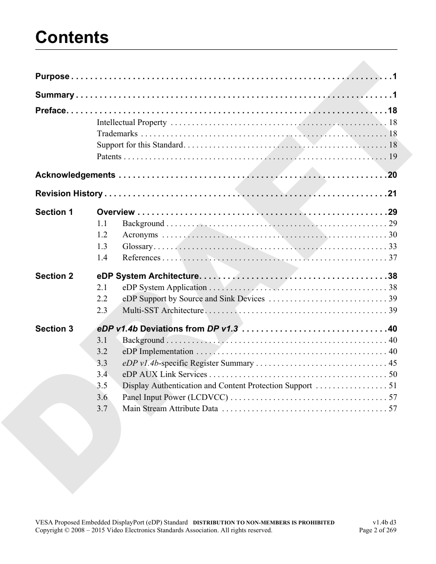
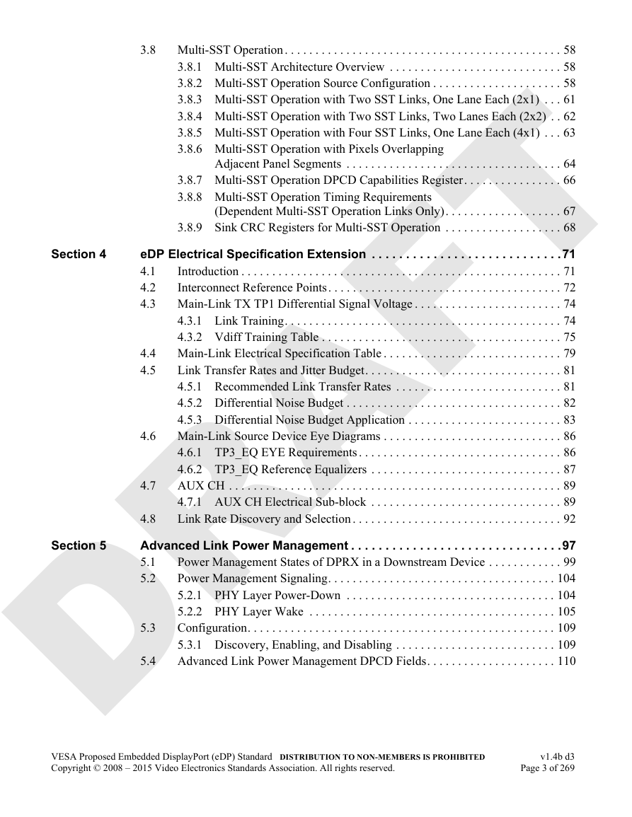
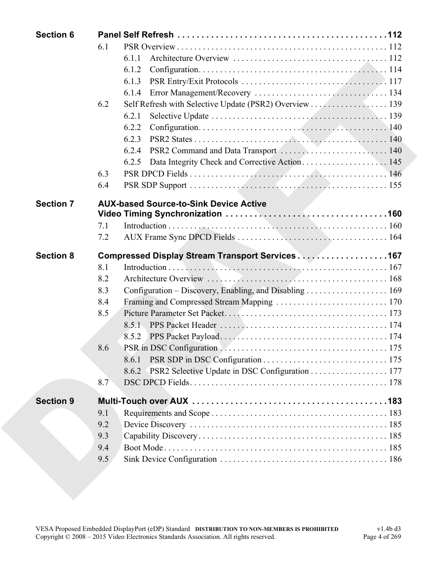
Contents
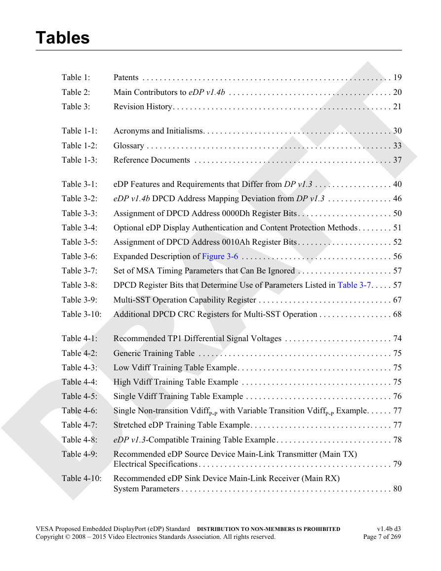
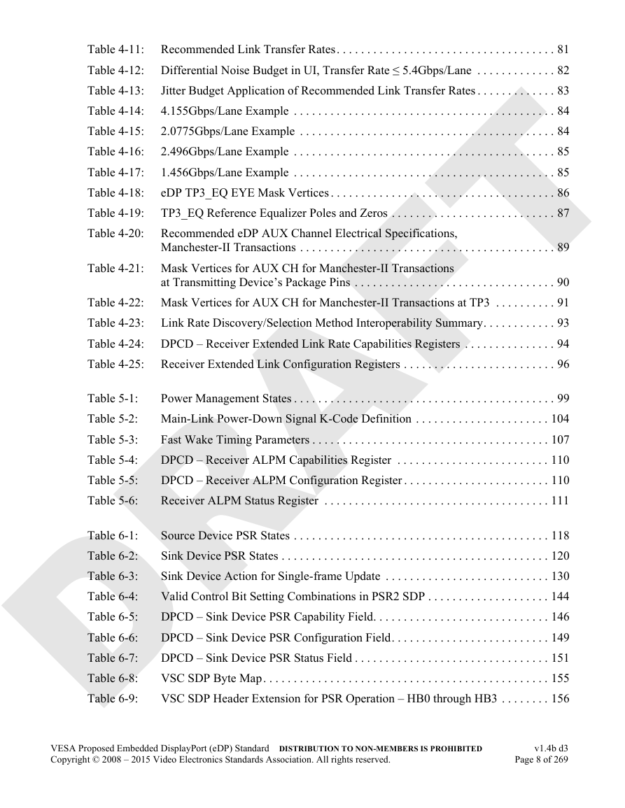
Tables
Figures
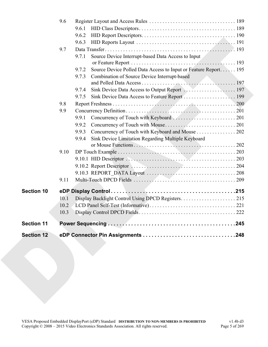
DPCD Registers that Differ from DP v1.3
Preface
1 Overview
1.1 Background
1.2 Acronyms
1.3 Glossary
1.4 References
2 eDP System Architecture
2.1 eDP System Application
2.2 eDP Support by Source and Sink Devices
2.3 Multi-SST Architecture
3 eDP v1.4b Deviations from DP v1.3
3.1 Background
3.2 eDP Implementation
3.3 eDP v1.4b-specific Register Summary
3.4 eDP AUX Link Services
3.5 Display Authentication and Content Protection Support
3.6 Panel Input Power (LCDVCC)
3.7 Main Stream Attribute Data
3.8 Multi-SST Operation
3.8.1 Multi-SST Architecture Overview
3.8.2 Multi-SST Operation Source Configuration
3.8.3 Multi-SST Operation with Two SST Links, One Lane Each (2x1)
3.8.4 Multi-SST Operation with Two SST Links, Two Lanes Each (2x2)
3.8.5 Multi-SST Operation with Four SST Links, One Lane Each (4x1)
3.8.6 Multi-SST Operation with Pixels Overlapping Adjacent Panel Segments
3.8.7 Multi-SST Operation DPCD Capabilities Register
3.8.8 Multi-SST Operation Timing Requirements (Dependent Multi-SST Operation Links Only)
3.8.9 Sink CRC Registers for Multi-SST Operation
4 eDP Electrical Specification Extension
4.1 Introduction
4.2 Interconnect Reference Points
4.3 Main-Link TX TP1 Differential Signal Voltage
4.3.1 Link Training
4.3.2 Vdiff Training Table
4.3.2.1 Special Training Tables
4.3.2.1.1 Rules for Custom Training Tables
4.3.2.1.2 Special Training Table Examples
4.4 Main-Link Electrical Specification Table
4.5 Link Transfer Rates and Jitter Budget
4.5.1 Recommended Link Transfer Rates
4.5.2 Differential Noise Budget
4.5.3 Differential Noise Budget Application
4.5.3.1 Custom Link Transfer Rates
4.5.3.1.1 Custom Transfer Rate Example 1 – 1920x1080 CVT Reduced Blanking, 24bpp Using a Single eDP Lane
4.5.3.1.2 Custom Transfer Rate Example 2 – 1920x1080 CVT Reduced Blanking, 24bpp Using Two eDP Lanes
4.5.3.1.3 Custom Transfer Rate Example 3 – Handheld with 19.2MHz Reference Clock
4.5.3.1.4 Custom Transfer Rate Example 4 – Handheld with 26MHz Reference Clock
4.6 Main-Link Source Device Eye Diagrams
4.6.1 TP3_EQ EYE Requirements
4.6.2 TP3_EQ Reference Equalizers
4.7 AUX CH
4.7.1 AUX CH Electrical Sub-block
4.7.1.1 Differential Voltage/Timing (EYE) Diagram for Manchester-II Transactions
4.8 Link Rate Discovery and Selection
5 Advanced Link Power Management
5.1 Power Management States of DPRX in a Downstream Device
5.2 Power Management Signaling
5.2.1 PHY Layer Power-Down
5.2.2 PHY Layer Wake
5.3 Configuration
5.3.1 Discovery, Enabling, and Disabling
5.4 Advanced Link Power Management DPCD Fields
6 Panel Self Refresh
6.1 PSR Overview
6.1.1 Architecture Overview
6.1.1.1 Source Device Responsibilities
6.1.1.2 Sink Device Responsibilities
6.1.2 Configuration
6.1.3 PSR Entry/Exit Protocols
6.1.3.1 PSR States
6.1.3.1.1 Source Device PSR States
6.1.3.1.2 Sink Device PSR States
6.1.3.2 PSR Entry
6.1.3.2.1 PSR Entry Link Management
6.1.3.2.1.1 Source Device Transmitter OFF
6.1.3.2.1.2 Source Device Transmitter Active
6.1.3.3 PSR Exit
6.1.3.3.1 PSR Exit Link Management
6.1.3.3.1.1 Source Device Main-Link Transmitter Is Turned OFF
6.1.3.3.1.2 Source Device Main-Link Transmitter Is Active
6.1.3.4 PSR Entry Abort
6.1.3.5 Single-frame Updates
6.1.3.5.1 Source Device Transmitter OFF
6.1.3.5.2 Source Device Transmitter Active
6.1.3.5.3 PSR Exit after Single-frame Update
6.1.3.5.4 Single-frame Update Immediately after PSR Entry
6.1.3.6 Burst Single-frame Updates
6.1.4 Error Management/Recovery
6.1.4.1 CRC Verification Performed in Source Device
6.1.4.2 CRC Verification Performed in Sink Device
6.2 Self Refresh with Selective Update (PSR2) Overview
6.2.1 Selective Update
6.2.2 Configuration
6.2.3 PSR2 States
6.2.4 PSR2 Command and Data Transport
6.2.5 Data Integrity Check and Corrective Action
6.3 PSR DPCD Fields
6.4 PSR SDP Support
7 AUX-based Source-to-Sink Device Active Video Timing Synchronization
7.1 Introduction
7.2 AUX Frame Sync DPCD Fields
8 Compressed Display Stream Transport Services
8.1 Introduction
8.2 Architecture Overview
8.3 Configuration – Discovery, Enabling, and Disabling
8.4 Framing and Compressed Stream Mapping
8.5 Picture Parameter Set Packet
8.5.1 PPS Packet Header
8.5.2 PPS Packet Payload
8.6 PSR in DSC Configuration
8.6.1 PSR SDP in DSC Configuration
8.6.2 PSR2 Selective Update in DSC Configuration
8.7 DSC DPCD Fields
9 Multi-Touch over AUX
9.1 Requirements and Scope
9.2 Device Discovery
9.3 Capability Discovery
9.4 Boot Mode
9.5 Sink Device Configuration
9.6 Register Layout and Access Rules
9.6.1 HID Class Descriptors
9.6.2 HID Report Descriptors
9.6.3 HID Reports Layout
9.6.3.1 Touch Sink Device Generated Reports
9.6.3.2 Touch Source Device Generated Reports
9.6.3.3 Report IDs
9.7 Data Transfer
9.7.1 Source Device Interrupt-based Data Access to Input or Feature Report
9.7.2 Source Device Polled Data Access to Input or Feature Report
9.7.3 Combination of Source Device Interrupt-based and Polled Data Access
9.7.4 Sink Device Data Access to Output Report
9.7.5 Sink Device Data Access to Feature Report
9.8 Report Freshness
9.9 Concurrency Definition
9.9.1 Concurrency of Touch with Keyboard
9.9.2 Concurrency of Touch with Mouse
9.9.3 Concurrency of Touch with Keyboard and Mouse
9.9.4 Sink Device Limitation Regarding Multiple Keyboard or Mouse Functions
9.10 DP Touch Example
9.10.1 HID Descriptor
9.10.2 Report Descriptor
9.10.3 REPORT_DATA Layout
9.11 Multi-Touch DPCD Fields
10 eDP Display Control
10.1 Display Backlight Control Using DPCD Registers
10.2 LCD Panel Self-Test (Informative)
10.3 Display Control DPCD Fields
11 Power Sequencing
12 eDP Connector Pin Assignments
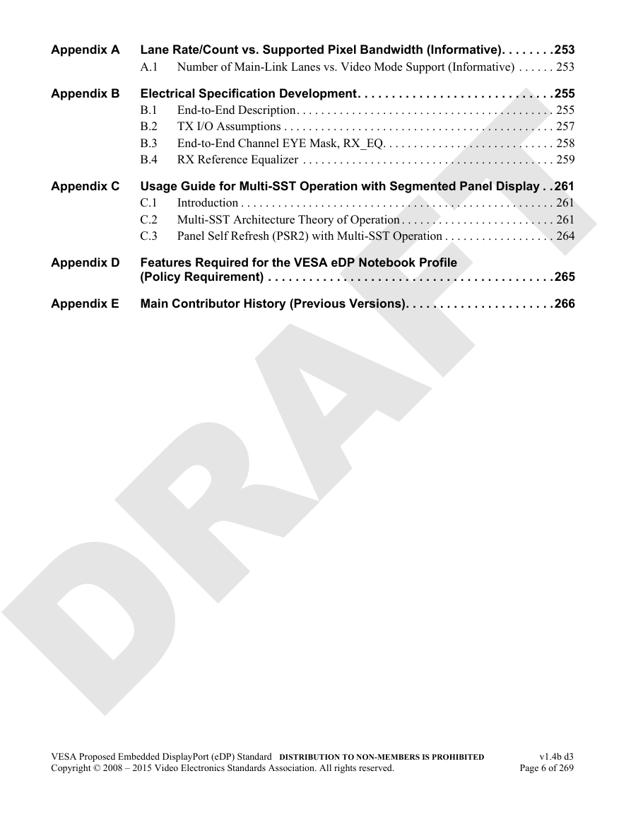
A Lane Rate/Count vs. Supported Pixel Bandwidth (Informative)
A.1 Number of Main-Link Lanes vs. Video Mode Support (Informative)
B Electrical Specification Development
B.1 End-to-End Description
B.2 TX I/O Assumptions
B.3 End-to-End Channel EYE Mask, RX_EQ
B.4 RX Reference Equalizer
C Usage Guide for Multi-SST Operation with Segmented Panel Display
C.1 Introduction
C.2 Multi-SST Architecture Theory of Operation
C.3 Panel Self Refresh (PSR2) with Multi-SST Operation
D Features Required for the VESA eDP Notebook Profile (Policy Requirement)
E Main Contributor History (Previous Versions)


 2023年江西萍乡中考道德与法治真题及答案.doc
 2012年重庆南川中考生物真题及答案.doc
 2013年江西师范大学地理学综合及文艺理论基础考研真题.doc
 2020年四川甘孜小升初语文真题及答案I卷.doc
 2020年注册岩土工程师专业基础考试真题及答案.doc
 2023-2024学年福建省厦门市九年级上学期数学月考试题及答案.doc
 2021-2022学年辽宁省沈阳市大东区九年级上学期语文期末试题及答案.doc
 2022-2023学年北京东城区初三第一学期物理期末试卷及答案.doc
 2018上半年江西教师资格初中地理学科知识与教学能力真题及答案.doc
 2012年河北国家公务员申论考试真题及答案-省级.doc
 2020-2021学年江苏省扬州市江都区邵樊片九年级上学期数学第一次质量检测试题及答案.doc
 2022下半年黑龙江教师资格证中学综合素质真题及答案.doc