S32K1xx Reference Manual (Supports S32K116, S32K118, S32K142, S32K144, S32K146, and S32K148)
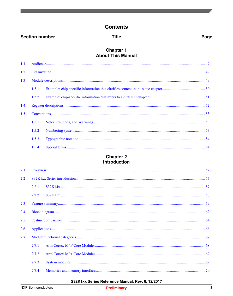
Contents
Chapter 1: About This Manual
Audience
Organization
Module descriptions
Example: chip-specific information that clarifies content in the same chapter
Example: chip-specific information that refers to a different chapter
Register descriptions
Conventions
Notes, Cautions, and Warnings
Numbering systems
Typographic notation
Special terms
Chapter 2: Introduction
Overview
S32K1xx Series introduction
S32K14x
S32K11x
Feature summary
Block diagram
Feature comparison
Applications
Module functional categories
Arm Cortex-M4F Core Modules
Arm Cortex-M0+ Core Modules
System modules
Memories and memory interfaces
Power Management
Clocking
Analog modules
Timer modules
Communication interfaces
Debug modules
Chapter 3: Memory Map
Introduction
SRAM memory map
Flash memory map
Peripheral bridge (AIPS-Lite) memory map
Read-after-write sequence and required serialization of memory operations
Private Peripheral Bus (PPB) memory map
Aliased bit-band regions for CM4 core
Chapter 4: Signal Multiplexing and Pin Assignment
Introduction
Functional description
Pad description
Default pad state
Signal Multiplexing sheet
IO Signal Table
Input muxing table
Pinout diagrams
Chapter 5: Security Overview
Introduction
Device security
Flash memory security
Flash memory security interactions with debug
Cryptographic Services Engine (CSEc) security features
Device Boot modes
Security use case examples
Secure boot: check bootloader for integrity and authenticity
Chain of trust: check flash memory for integrity and authenticity
Secure communication
Component protection
Message-authentication example
Steps required before failure analysis
Security programming flow example (Secure Boot)
Chapter 6: Safety Overview
Introduction
S32K1xx safety concept
Cortex-M4/M0+ Structural Core Self Test (SCST)
ECC on RAM and flash memory
Power supply monitoring
Clock monitoring
Temporal protection
Operational interference protection
System Memory Protection Unit (MPU)
Peripheral protection
Register protection
CRC
Diversity of system resources
Chapters 7-23 Core and System Modules
Chapter 7: CM4 Overview
Arm Cortex-M4F core configuration
Buses, interconnects, and interfaces
System Tick Timer
Debug facilities
Caches
Core privilege levels
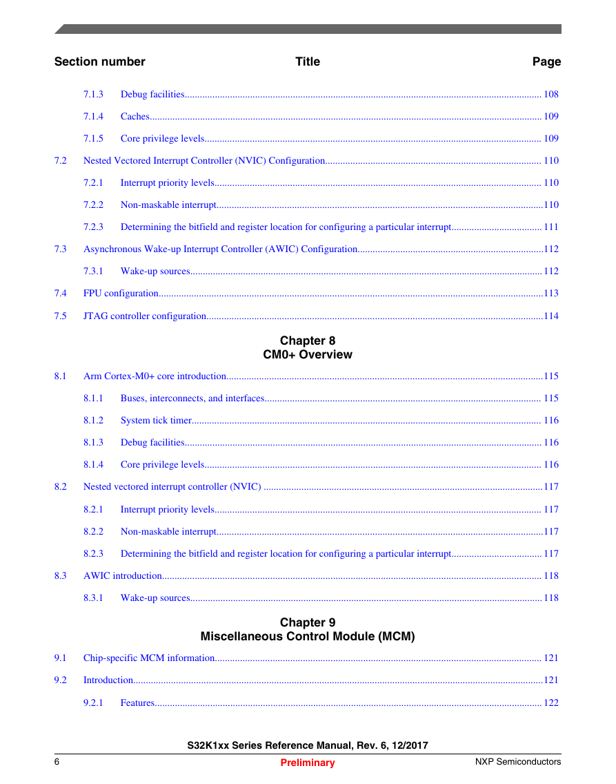
Nested Vectored Interrupt Controller (NVIC) Configuration
Interrupt priority levels
Non-maskable interrupt
Determining the bitfield and register location for configuring a particular interrupt
Asynchronous Wake-up Interrupt Controller (AWIC) Configuration
Wake-up sources
FPU configuration
JTAG controller configuration
Chapter 8: CM0+ Overview
Arm Cortex-M0+ core introduction
Buses, interconnects, and interfaces
System tick timer
Debug facilities
Core privilege levels
Nested vectored interrupt controller (NVIC)
Interrupt priority levels
Non-maskable interrupt
Determining the bitfield and register location for configuring a particular interrupt
AWIC introduction
Wake-up sources
Chapter 9: Miscellaneous Control Module (MCM)
Chip-specific MCM information
Introduction
Features
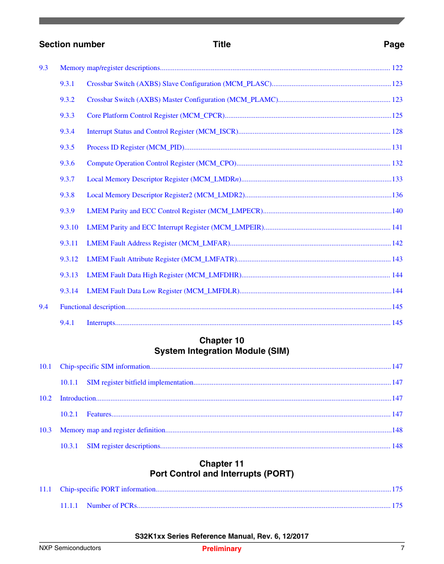
Memory map/register descriptions
MCM
MCM_PLASC
MCM_PLAMC
MCM_CPCR
MCM_ISCR
MCM_PID
MCM_CPO
MCM_LMDRn
MCM_LMDR2
MCM_LMPECR
MCM_LMPEIR
MCM_LMFAR
MCM_LMFATR
MCM_LMFDHR
MCM_LMFDLR
Functional description
Interrupts
Chapter 10: System Integration Module (SIM)
Chip-specific SIM information
SIM register bitfield implementation
Introduction
Features
Memory map and register definition
SIM register descriptions
SIM Memory map
Chip Control register (CHIPCTL)
FTM Option Register 0 (FTMOPT0)
LPO Clock Select Register (LPOCLKS)
ADC Options Register (ADCOPT)
FTM Option Register 1 (FTMOPT1)
Miscellaneous control register 0 (MISCTRL0)
System Device Identification Register (SDID)
Platform Clock Gating Control Register (PLATCGC)
Flash Configuration Register 1 (FCFG1)
Unique Identification Register High (UIDH)
Unique Identification Register Mid-High (UIDMH)
Unique Identification Register Mid Low (UIDML)
Unique Identification Register Low (UIDL)
System Clock Divider Register 4 (CLKDIV4)
Miscellaneous Control register 1 (MISCTRL1)
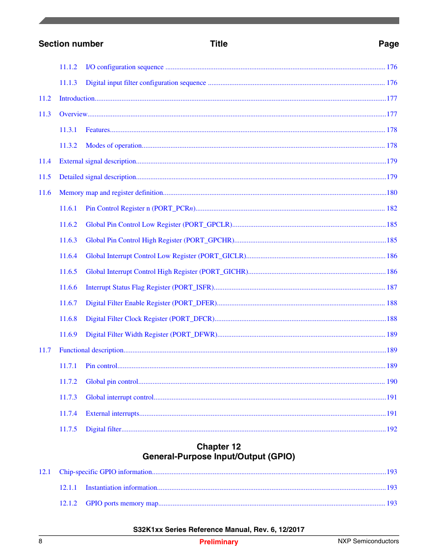
Chapter 11: Port Control and Interrupts (PORT)
Chip-specific PORT information
Number of PCRs
I/O configuration sequence
Digital input filter configuration sequence
Digital input filter configuration sequence while using GPIO interrupt
Digital input filter configuration sequence while using NMI
Introduction
Overview
Features
Modes of operation
Run mode
Wait mode
Stop mode
Debug mode
External signal description
Detailed signal description
Memory map and register definition
PORT
PORT_PCRn
PORT_GPCLR
PORT_GPCHR
PORT_GICLR
PORT_GICHR
PORT_ISFR
PORT_DFER
PORT_DFCR
PORT_DFWR
Functional description
Pin control
Global pin control
Global interrupt control
External interrupts
Digital filter
Chapter 12: General-Purpose Input/Output (GPIO)
Chip-specific GPIO information
Instantiation information
GPIO ports memory map
GPIO register reset values
Introduction
Features
Modes of operation
GPIO signal descriptions
Detailed signal description
Memory map and register definition
GPIO register descriptions
GPIO Memory map
Port Data Output Register (PDOR)
Port Set Output Register (PSOR)
Port Clear Output Register (PCOR)
Port Toggle Output Register (PTOR)
Port Data Input Register (PDIR)
Port Data Direction Register (PDDR)
Port Input Disable Register (PIDR)
Functional description
General-purpose input
General-purpose output
Chapter 13: Crossbar Switch Lite (AXBS-Lite)
Chip-specific AXBS-Lite information
Crossbar Switch master assignments
Crossbar Switch slave assignments
Introduction
Features
Functional Description
General operation
Arbitration
Arbitration during undefined length bursts
Fixed-priority operation
Round-robin priority operation
Initialization/application information
Chapter 14: Memory Protection Unit (MPU)
Chip-specific MPU information
MPU Slave Port Assignments
MPU Logical Bus Master Assignments
Current PID
Region descriptors and slave port configuration
Introduction
Overview
Block diagram
Features
MPU register descriptions
MPU Memory map
Control/Error Status Register (CESR)
Error Address Register, slave port n (EAR0 - EAR4)
Error Detail Register, slave port n (EDR0 - EDR4)
Region Descriptor n, Word 0 (RGD0_WORD0 - RGD15_WORD0)
Region Descriptor 0, Word 1 (RGD0_WORD1)
Region Descriptor 0, Word 2 (RGD0_WORD2)
Region Descriptor 0, Word 3 (RGD0_WORD3)
Region Descriptor n, Word 1 (RGD1_WORD1 - RGD15_WORD1)
Region Descriptor n, Word 2 (RGD1_WORD2 - RGD15_WORD2)
Region Descriptor n, Word 3 (RGD1_WORD3 - RGD15_WORD3)
Region Descriptor Alternate Access Control 0 (RGDAAC0)
Region Descriptor Alternate Access Control n (RGDAAC1 - RGDAAC15)
Functional description
Access evaluation macro
Hit determination
Privilege violation determination
Putting it all together and error terminations
Power management
Initialization information
Application information
Chapter 15: Peripheral Bridge (AIPS-Lite)
Chip-specific AIPS information
Instantiation information
Memory maps
Introduction
Features
General operation
Memory map/register definition
AIPS register descriptions
AIPS Memory map
Master Privilege Register A (MPRA)
Peripheral Access Control Register (PACRA)
Peripheral Access Control Register (PACRB)
Peripheral Access Control Register (PACRD)
Off-Platform Peripheral Access Control Register (OPACRA)
Off-Platform Peripheral Access Control Register (OPACRB)
Off-Platform Peripheral Access Control Register (OPACRC)
Off-Platform Peripheral Access Control Register (OPACRD)
Off-Platform Peripheral Access Control Register (OPACRE)
Off-Platform Peripheral Access Control Register (OPACRF)
Off-Platform Peripheral Access Control Register (OPACRG)
Off-Platform Peripheral Access Control Register (OPACRH)
Off-Platform Peripheral Access Control Register (OPACRI)
Off-Platform Peripheral Access Control Register (OPACRJ)
Off-Platform Peripheral Access Control Register (OPACRK)
Off-Platform Peripheral Access Control Register (OPACRL)
Functional description
Access support
Chapter 16: Direct Memory Access Multiplexer (DMAMUX)
Chip-specific DMAMUX information
Number of channels
DMA transfers via TRGMUX trigger
Introduction
Overview
Features
Modes of operation
External signal description
Memory map/register definition
DMAMUX register descriptions
DMAMUX Memory map
Channel Configuration register (CHCFG0 - CHCFG15)
Functional description
DMA channels with periodic triggering capability
DMA channels with no triggering capability
Always-enabled DMA sources
Initialization/application information
Reset
Enabling and configuring sources
Chapter 17: Enhanced Direct Memory Access (eDMA)
Chip-specific eDMA information
Number of channels
Introduction
eDMA system block diagram
Block parts
Features
Modes of operation
Memory map/register definition
TCD memory
TCD initialization
TCD structure
Reserved memory and bit fields
DMA register descriptions
DMA Memory map
Control Register (CR)
Error Status Register (ES)
Enable Request Register (ERQ)
Enable Error Interrupt Register (EEI)
Clear Enable Error Interrupt Register (CEEI)
Set Enable Error Interrupt Register (SEEI)
Clear Enable Request Register (CERQ)
Set Enable Request Register (SERQ)
Clear DONE Status Bit Register (CDNE)
Set START Bit Register (SSRT)
Clear Error Register (CERR)
Clear Interrupt Request Register (CINT)
Interrupt Request Register (INT)
Error Register (ERR)
Hardware Request Status Register (HRS)
Enable Asynchronous Request in Stop Register (EARS)
Channel Priority Register (DCHPRI0 - DCHPRI15)
TCD Source Address (TCD0_SADDR - TCD15_SADDR)
TCD Signed Source Address Offset (TCD0_SOFF - TCD15_SOFF)
TCD Transfer Attributes (TCD0_ATTR - TCD15_ATTR)
TCD Minor Byte Count (Minor Loop Mapping Disabled) (TCD0_NBYTES_MLNO - TCD15_NBYTES_MLNO)
TCD Signed Minor Loop Offset (Minor Loop Mapping Enabled and Offset Disabled) (TCD0_NBYTES_MLOFFNO - TCD15_NBYTES_MLOFFNO)
TCD Signed Minor Loop Offset (Minor Loop Mapping and Offset Enabled) (TCD0_NBYTES_MLOFFYES - TCD15_NBYTES_MLOFFYES)
TCD Last Source Address Adjustment (TCD0_SLAST - TCD15_SLAST)
TCD Destination Address (TCD0_DADDR - TCD15_DADDR)
TCD Signed Destination Address Offset (TCD0_DOFF - TCD15_DOFF)
TCD Current Minor Loop Link, Major Loop Count (Channel Linking Disabled) (TCD0_CITER_ELINKNO - TCD15_CITER_ELINKNO)
TCD Current Minor Loop Link, Major Loop Count (Channel Linking Enabled) (TCD0_CITER_ELINKYES - TCD15_CITER_ELINKYES)
TCD Last Destination Address Adjustment/Scatter Gather Address (TCD0_DLASTSGA - TCD15_DLASTSGA)
TCD Control and Status (TCD0_CSR - TCD15_CSR)
TCD Beginning Minor Loop Link, Major Loop Count (Channel Linking Disabled) (TCD0_BITER_ELINKNO - TCD15_BITER_ELINKNO)
TCD Beginning Minor Loop Link, Major Loop Count (Channel Linking Enabled) (TCD0_BITER_ELINKYES - TCD15_BITER_ELINKYES)
Functional description
eDMA basic data flow
Fault reporting and handling
Channel preemption
Initialization/application information
eDMA initialization
Programming errors
Arbitration mode considerations
Fixed channel arbitration
Round-robin channel arbitration
Performing DMA transfers
Single request
Multiple requests
Using the modulo feature
Monitoring transfer descriptor status
Testing for minor loop completion
Reading the transfer descriptors of active channels
Checking channel preemption status
Channel Linking
Dynamic programming
Dynamically changing the channel priority
Dynamic channel linking
Dynamic scatter/gather
Method 1 (channel not using major loop channel linking)
Method 2 (channel using major loop channel linking)
Suspend/resume a DMA channel with active hardware service requests
Suspend an active DMA channel
Resume a DMA channel
Chapter 18: Trigger MUX Control (TRGMUX)
Chip-specific TRGMUX information
Module interconnectivity
TRGMUX register information
Introduction
Features
Memory map and register definition
TRGMUX register descriptions
TRGMUX Memory map
TRGMUX DMAMUX0 Register (DMAMUX0)
TRGMUX EXTOUT0 Register (EXTOUT0)
TRGMUX EXTOUT1 Register (EXTOUT1)
TRGMUX ADC0 Register (ADC0)
TRGMUX ADC1 Register (ADC1)
TRGMUX CMP0 Register (CMP0)
TRGMUX FTM0 Register (FTM0)
TRGMUX FTM1 Register (FTM1)
TRGMUX FTM2 Register (FTM2)
TRGMUX FTM3 Register (FTM3)
TRGMUX PDB0 Register (PDB0)
TRGMUX PDB1 Register (PDB1)
TRGMUX FLEXIO Register (FLEXIO)
TRGMUX LPIT0 Register (LPIT0)
TRGMUX LPUART0 Register (LPUART0)
TRGMUX LPUART1 Register (LPUART1)
TRGMUX LPI2C0 Register (LPI2C0)
TRGMUX LPSPI0 Register (LPSPI0)
TRGMUX LPSPI1 Register (LPSPI1)
TRGMUX LPTMR0 Register (LPTMR0)
TRGMUX LPI2C1 Register (LPI2C1)
TRGMUX FTM4 Register (FTM4)
TRGMUX FTM5 Register (FTM5)
TRGMUX FTM6 Register (FTM6)
TRGMUX FTM7 Register (FTM7)
Chapter 19: External Watchdog Monitor (EWM)
Chip-specific EWM information
EWM_OUT signal configuration
EWM Memory Map access
EWM low-power modes
Introduction
Features
Modes of Operation
Stop Mode
Debug Mode
Block Diagram
EWM Signal Descriptions
Memory Map/Register Definition
EWM register descriptions
EWM Memory map
Control Register (CTRL)
Service Register (SERV)
Compare Low Register (CMPL)
Compare High Register (CMPH)
Clock Prescaler Register (CLKPRESCALER)
Functional Description
The EWM_OUT_b Signal
EWM_OUT_b pin state in low power modes
The EWM_in Signal
EWM Counter
EWM Compare Registers
EWM Refresh Mechanism
EWM Interrupt
Counter clock prescaler
Chapter 20: Error Injection Module (EIM)
Chip-specific EIM information
EIM channel assignments
Introduction
Overview
Features
EIM register descriptions
EIM Memory map
Error Injection Module Configuration Register (EIMCR)
Error Injection Channel Enable register (EICHEN)
Error Injection Channel Descriptor n, Word0 (EICHD0_WORD0 - EICHD1_WORD0)
Error Injection Channel Descriptor n, Word1 (EICHD0_WORD1 - EICHD1_WORD1)
Functional description
Chapter 21: Error Reporting Module (ERM)
Chip-specific ERM information
Sources of memory error events
Introduction
Overview
Features
ERM register descriptions
ERM Memory map
ERM Configuration Register 0 (CR0)
ERM Status Register 0 (SR0)
ERM Memory n Error Address Register (EAR0 - EAR1)
Functional description
Single-bit correction events
Non-correctable error events
Initialization
Chapter 22: Watchdog timer (WDOG)
Chip-specific WDOG information
WDOG clocks
WDOG low-power modes
Default watchdog timeout
Introduction
Features
Block diagram
Memory map and register definition
WDOG register descriptions
WDOG Memory map
Watchdog Control and Status Register (CS)
Watchdog Counter Register (CNT)
Watchdog Timeout Value Register (TOVAL)
Watchdog Window Register (WIN)
Functional description
Clock source
Watchdog refresh mechanism
Window mode
Refreshing the Watchdog
Using interrupts to delay resets
Backup reset
Functionality in debug and low-power modes
Fast testing of the watchdog
Testing each byte of the counter
Entering user mode
Application Information
Chapter 23: Cyclic Redundancy Check (CRC)
Chip-specific CRC information
Introduction
Features
Block diagram
Modes of operation
Run mode
Low-power modes (Stop)
Memory map and register descriptions
CRC register descriptions
CRC Memory map
CRC Data register (DATA)
CRC Polynomial register (GPOLY)
CRC Control register (CTRL)
Functional description
CRC initialization/reinitialization
CRC calculations
16-bit CRC
32-bit CRC
Transpose feature
Types of transpose
CRC result complement
Chapters 24-25 Reset and Boot
Chapter 24: Reset and Boot
Introduction
Reset
Power-on reset (POR)
System reset sources
External pin reset
RESET_B pin filter
Low voltage detect (LVD)
Watchdog reset
Loss-of-clock (LOC) reset
Loss-of-lock (LOL) reset
Stop mode acknowledge error (SACKERR)
Software reset (SW)
Lockup reset (LOCKUP)
MDM-AP system reset request
MCU Resets
Reset pin
Debug resets
JTAG reset
Resetting the debug subsystem
Boot
Boot sources
FOPT boot options
Boot sequence
Chapter 25: Reset Control Module (RCM)
Chip-specific RCM information
RCM register information
Reset pin filter operation in STOP1/2 modes
Introduction
Reset memory map and register descriptions
RCM
RCM_VERID
RCM_PARAM
RCM_SRS
RCM_RPC
RCM_SSRS
RCM_SRIE
Chapters 26-29 Clocking
Chapter 26: Clock Distribution
Introduction
High level clocking diagram
Clock definitions
Internal clocking requirements
Clock divider values after reset
HSRUN mode clocking
VLPR mode clocking
VLPR/VLPS mode entry
Clock Gating
Module clocks
Chapter 27: System Clock Generator (SCG)
Chip-specific SCG information
Introduction
Features
Memory Map/Register Definition
SCG
SCG_VERID
SCG_PARAM
SCG_CSR
SCG_RCCR
SCG_VCCR
SCG_HCCR
SCG_CLKOUTCNFG
SCG_SOSCCSR
SCG_SOSCDIV
SCG_SOSCCFG
SCG_SIRCCSR
SCG_SIRCDIV
SCG_SIRCCFG
SCG_FIRCCSR
SCG_FIRCDIV
SCG_FIRCCFG
SCG_SPLLCSR
SCG_SPLLDIV
SCG_SPLLCFG
Functional description
SCG Clock Mode Transitions
Chapter 28: Peripheral Clock Controller (PCC)
Chip-specific PCC information
PCC register information
PCC CMU0 Register (PCC_CMU0)
PCC CMU1 Register (PCC_CMU1)
Introduction
Features
Functional description
Memory map and register definition
PCC register descriptions
PCC Memory map
PCC FTFC Register (PCC_FTFC)
PCC DMAMUX Register (PCC_DMAMUX)
PCC FlexCAN0 Register (PCC_FlexCAN0)
PCC FlexCAN1 Register (PCC_FlexCAN1)
PCC FTM3 Register (PCC_FTM3)
PCC ADC1 Register (PCC_ADC1)
PCC FlexCAN2 Register (PCC_FlexCAN2)
PCC LPSPI0 Register (PCC_LPSPI0)
PCC LPSPI1 Register (PCC_LPSPI1)
PCC LPSPI2 Register (PCC_LPSPI2)
PCC PDB1 Register (PCC_PDB1)
PCC CRC Register (PCC_CRC)
PCC PDB0 Register (PCC_PDB0)
PCC LPIT Register (PCC_LPIT)
PCC FTM0 Register (PCC_FTM0)
PCC FTM1 Register (PCC_FTM1)
PCC FTM2 Register (PCC_FTM2)
PCC ADC0 Register (PCC_ADC0)
PCC RTC Register (PCC_RTC)
PCC LPTMR0 Register (PCC_LPTMR0)
PCC PORTA Register (PCC_PORTA)
PCC PORTB Register (PCC_PORTB)
PCC PORTC Register (PCC_PORTC)
PCC PORTD Register (PCC_PORTD)
PCC PORTE Register (PCC_PORTE)
PCC SAI0 Register (PCC_SAI0)
PCC SAI1 Register (PCC_SAI1)
PCC FlexIO Register (PCC_FlexIO)
PCC EWM Register (PCC_EWM)
PCC LPI2C0 Register (PCC_LPI2C0)
PCC LPI2C1 Register (PCC_LPI2C1)
PCC LPUART0 Register (PCC_LPUART0)
PCC LPUART1 Register (PCC_LPUART1)
PCC LPUART2 Register (PCC_LPUART2)
PCC FTM4 Register (PCC_FTM4)
PCC FTM5 Register (PCC_FTM5)
PCC FTM6 Register (PCC_FTM6)
PCC FTM7 Register (PCC_FTM7)
PCC CMP0 Register (PCC_CMP0)
PCC QSPI Register (PCC_QSPI)
PCC ENET Register (PCC_ENET)
Chapter 29: Clock Monitoring Unit (CMU)
CMU chip-specific information
Introduction
Basic operation
Main features
CMU-FC register descriptions
CMU-FC Memory map
CMU Frequency Check Global Configuration Register (GCR)
CMU Frequency Check Reference Count Configuration Register (RCCR)
CMU Frequency Check High Threshold Configuration Register (HTCR)
CMU Frequency Check Low Threshold Configuration Register (LTCR)
CMU Frequency Check Status Register (SR)
CMU Frequency Check Interrupt/Event Enable Register (IER)
Monitored clock lost
Functional description
Programming guidelines
Programming HFREF and LFREF
Programming CMU_FC_RCCR[REF_CNT]
Module Programming Sequence
Chapters 30-36 Memories and Memory Interfaces
Chapter 30: Memories and Memory Interfaces
Introduction
Flash Memory Controller and flash memory modules
SRAM configuration
SRAM sizes
SRAM accessibility
SRAM arbitration and priority control
SRAM retention: power modes and resets
Chapter 31: PRAM Controller (PRAMC)
PRAMC chip-specific information
Introduction
Memory map and register definition
Functional description
Error Correcting Code (ECC)
Overview
Read/Write introduction
Reads
Unaligned reads
ECC errors on reads
Optional read wait-state
Reads and ECC events
Writes
32-bit writes
Less than 32-bit writes
Unaligned writes
Late write hits
Initialization / Application information
Chapter 32: Local Memory Controller (LMEM)
Chip-specific LMEM information
LMEM region description
LMEM SRAM sizes
Introduction
Block Diagram
Cache features
Memory Map/Register Definition
LMEM register descriptions
LMEM Memory map
Cache control register (PCCCR)
Cache line control register (PCCLCR)
Cache search address register (PCCSAR)
Cache read/write value register (PCCCVR)
Cache regions mode register (PCCRMR)
Functional Description
LMEM Function
SRAM Function
SRAM Configuration
SRAM Arrays
SRAM Accesses
Cache Function
Cache Control
Cache set commands
Cache line commands
Chapter 33: Miscellaneous System Control Module (MSCM)
Chip-specific MSCM information
Chip-specific TMLSZ/TMUSZ information
Chip-specific register information
Overview
Chip Configuration and Boot
MSCM Memory Map/Register Definition
CPU Configuration Memory Map and Registers
MSCM register descriptions
MSCM Memory map
Processor X Type Register (CPxTYPE)
Processor X Number Register (CPxNUM)
Processor X Master Register (CPxMASTER)
Processor X Count Register (CPxCOUNT)
Processor X Configuration Register 0 (CPxCFG0)
Processor X Configuration Register 1 (CPxCFG1)
Processor X Configuration Register 2 (CPxCFG2)
Processor X Configuration Register 3 (CPxCFG3)
Processor 0 Type Register (CP0TYPE)
Processor 0 Number Register (CP0NUM)
Processor 0 Master Register (CP0MASTER)
Processor 0 Count Register (CP0COUNT)
Processor 0 Configuration Register 0 (CP0CFG0)
Processor 0 Configuration Register 1 (CP0CFG1)
Processor 0 Configuration Register 2 (CP0CFG2)
Processor 0 Configuration Register 3 (CP0CFG3)
On-Chip Memory Descriptor Register (OCMDR0)
On-Chip Memory Descriptor Register (OCMDR1)
On-Chip Memory Descriptor Register (OCMDR2)
Chapter 34: Flash Memory Controller (FMC)
Chip-specific FMC information
FMC masters
Program flash and Data flash port width
Introduction
Overview
Features
Modes of operation
External signal description
Functional description
Default configuration
Speculative reads
Initialization and application information
Chapter 35: Flash Memory Module (FTFC)
Chip-specific FTFC information
Flash memory types
Flash memory sizes
128 KB program flash / 32 KB FlexNVM / 2 KB FlexRAM module
Emulated EEPROM data set size (EEESIZE)
FlexNVM partition code (DEPART)
256 KB program flash / 32 KB FlexNVM / 2 KB FlexRAM module
Emulated EEPROM data set size (EEESIZE)
FlexNVM partition code (DEPART)
256 KB program flash / 64 KB FlexNVM / 4 KB FlexRAM module
Emulated EEPROM data set size (EEESIZE)
FlexNVM partition code (DEPART)
512 KB program flash / 64 KB FlexNVM / 4 KB FlexRAM module
Emulated EEPROM data set size (EEESIZE)
FlexNVM partition code (DEPART)
1 MB program flash / 256 KB FlexNVM / 4 KB FlexRAM module
Emulated EEPROM data set size (EEESIZE)
FlexNVM partition code (DEPART)
2 MB program flash / 256 KB FlexNVM / 4 KB FlexRAM module
Emulated EEPROM data set size (EEESIZE)
FlexNVM partition code (DEPART)
Flash memory map
Flash memory security
Power mode restrictions on flash memory programming
Flash memory modes
Erase all contents of flash memory
Customize MCU operations via FTFC_FOPT register
Simultaneous operations on PFLASH read partitions
Introduction
Features
Program flash memory features
FlexNVM memory features
FlexRAM features
Cryptographic Services Engine (CSEc) module features
Other FTFC module features
Block diagram
Glossary
External signal description
Memory map and registers
Flash configuration field description
Program flash 0 IFR map
Program Once field
Data flash 0 IFR map
EEPROM data set size
FlexNVM partition code
Register descriptions
FTFC register descriptions
FTFC Memory map
Flash Status Register (FSTAT)
Flash Configuration Register (FCNFG)
Flash Security Register (FSEC)
Flash Option Register (FOPT)
Flash Common Command Object Registers (FCCOB0 - FCCOBB)
Program Flash Protection Registers (FPROT0 - FPROT3)
EEPROM Protection Register (FEPROT)
Data Flash Protection Register (FDPROT)
Flash CSEc Status Register (FCSESTAT)
Flash Error Status Register (FERSTAT)
Flash Error Configuration Register (FERCNFG)
Functional description
Flash protection
FlexNVM description
FlexNVM block partitioning for FlexRAM
EEPROM user perspective
EEPROM implementation overview
Write endurance to FlexRAM for emulated EEPROM
ECC implementation for FlexNVM
Interrupts
Flash operation in low-power modes
Wait mode
Stop mode
Functional modes of operation
Flash memory reads and ignored writes
Read while write (RWW)
Flash program and erase
FTFC command operations
Command write sequence
Load the FCCOB registers
Launch the command by clearing CCIF
Command execution and error reporting
Flash commands
Flash commands by mode
Allowed simultaneous flash operations
Margin read commands
Flash command descriptions
Read 1s Block command
Read 1s Section command
Program Check command
Program Phrase command
Erase Flash Block command
Erase Flash Sector command
Suspending an Erase Flash Sector operation
Resuming a suspended Erase Flash Sector operation
Aborting a suspended Erase Flash Sector operation
Program Section command
Flash sector programming
Read 1s All Blocks command
Read Once command
Program Once command
Erase All Blocks command
Triggering an erase all external to the flash module
Verify Backdoor Access Key command
Erase All Blocks Unsecure command
Program Partition command
Set FlexRAM Function command
Security
FTFC access by mode and security
Changing the security state
Un-securing the MCU using backdoor key access
Cryptographic Services Engine (CSEc)
Key/seed/random number generation
Secure boot mode
User CSEc command interface and command set
CSEc command header
Generic PRAM interface description
CMD_ENC_ECB
CMD_ENC_CBC
CMD_DEC_ECB
CMD_DEC_CBC
CMD_GENERATE_MAC
CSEc format for CMD_GENERATE_MAC (pointer method)
CMD_VERIFY_MAC
CMD_VERIFY_MAC - CSEc format (pointer method)
CMD_LOAD_KEY
CMD_LOAD_PLAIN_KEY
CMD_EXPORT_RAM_KEY
CMD_INIT_RNG
CMD_EXTEND_SEED
CMD_RND
CMD_SECURE_BOOT
CMD_BOOT_FAILURE
CMD_BOOT_OK
CMD_GET_STATUS
CMD_GET_ID
CMD_CANCEL
CMD_BOOT_DEFINE
CMD_DBG_CHAL
CMD_DBG_AUTH
CMD_MP_COMPRESS
Reset sequence
Chapter 36: Quad Serial Peripheral Interface (QuadSPI)
Chip-specific QuadSPI information
Overview
Memory size requirement
QuadSPI register reset values
Use case
Supported read modes
External memory options
Recommended software configuration
Recommended programming sequence
Clock ratio between QuadSPI clocks
QuadSPI_MCR[SCLKCFG] implementation
QuadSPI_SOCCR[SOCCFG] implementation
Introduction
Features
Block Diagram
QuadSPI Modes of Operation
Acronyms and Abbreviations
Glossary for QuadSPI module
External Signal Description
Driving External Signals
Memory Map and Register Definition
Register Write Access
Peripheral Bus Register Descriptions
QuadSPI
QuadSPI_MCR
QuadSPI_IPCR
QuadSPI_FLSHCR
QuadSPI_BUF0CR
QuadSPI_BUF1CR
QuadSPI_BUF2CR
QuadSPI_BUF3CR
QuadSPI_BFGENCR
QuadSPI_SOCCR
QuadSPI_BUF0IND
QuadSPI_BUF1IND
QuadSPI_BUF2IND
QuadSPI_SFAR
QuadSPI_SFACR
QuadSPI_SMPR
QuadSPI_RBSR
QuadSPI_RBCT
QuadSPI_TBSR
QuadSPI_TBDR
QuadSPI_TBCT
QuadSPI_SR
QuadSPI_FR
QuadSPI_RSER
QuadSPI_SPNDST
QuadSPI_SPTRCLR
QuadSPI_SFA1AD
QuadSPI_SFA2AD
QuadSPI_SFB1AD
QuadSPI_SFB2AD
QuadSPI_RBDRn
QuadSPI_LUTKEY
QuadSPI_LCKCR
QuadSPI_LUTn
Serial Flash Address Assignment
Flash memory mapped AMBA bus
AHB Bus Access Considerations
Memory Mapped Serial Flash Data - Individual Flash Mode on Flash A
Memory Mapped Serial Flash Data - Individual Flash Mode on Flash B
AHB RX Data Buffer (QSPI_ARDB0 to QSPI_ARDB31)
ARDBn
Interrupt Signals
Functional Description
Serial Flash Access Schemes
Normal Mode
Programmable Sequence Engine
Flexible AHB buffers
Suspend-Abort Mechanism
HBURST Support
Look-up Table
Issuing Serial Flash Memory (SFM) Commands
Flash Programming
Flash Read
Byte Ordering of Serial Flash Read Data
Normal Mode Interrupt and DMA Requests
TX Buffer Operation
Address scheme
HyperRAM Support
Initialization/Application Information
Power Up and Reset
Available Status/Flag Information
IP Commands
AHB Commands
Overview of Error Flags
IP Bus and AHB Access Command Collisions
Exclusive Access to Serial Flash for AHB Commands
RX Buffer Read via QSPI_ARDB Registers
RX Buffer Read via QSPI_RBDR Registers
Command Arbitration
Flash Device Selection
DMA Usage
DMA Usage in Normal Mode
Bandwidth considerations
Byte Ordering - Endianness
Programming Flash Data
Reading Flash Data into the RX Buffer
Readout of the RX Buffer via QSPI_RBDRn
Readout of the RX Buffer via ARDBn
Reading Flash Data into the AHB Buffer
Readout of the AHB Buffer via Memory Mapped Read
Driving Flash Control Signals in Single and Dual Mode
Serial Flash Devices
Example Sequences
Read Command (Spansion Hyperflash/HyperRAM)
Read Status Register(Spansion Hyperflash/HyperRAM)
Word Program (Spansion Hyperflash/HyperRAM)
Fast Read Sequence (Macronix/Numonyx/Spansion/Winbond)
Fast Dual I/O DT Read Sequence (Macronix)
Fast Read Quad Output (Winbond)
4 x I/O Read Enhance Performance Mode (XIP) (Macronix)
Dual Command Page Program (Numonyx)
Sector Erase (Macronix/Spansion/Numonyx)
Read Status Register (Macronix/Spansion/Numonyx/Winbond)
Sampling of Serial Flash Input Data
Basic Description
Supported read modes
SDR mode
Internal sampling
DQS sampling method
DDR Mode
DQS sampling method
Data Strobe (DQS) sampling method
Basic Description
Internally generated DQS
External DQS
Data Input Hold Requirement of Flash
Chapters 37-39 Power Management
Chapter 37: Power Management
Introduction
Power modes description
Entering and exiting power modes
Clocking modes
Clock gating
Stop mode options
DMA wake-up
Compute Operation (CPO)
Peripheral Doze
Power mode transitions
Shutdown sequencing for power modes
Power mode restrictions on flash memory programming
Module operation in available low power modes
QuadSPI, Ethernet, and SAI operation
Chapter 38: System Mode Controller (SMC)
Introduction
Modes of operation
Memory map and register descriptions
SMC
SMC_VERID
SMC_PARAM
SMC_PMPROT
SMC_PMCTRL
SMC_ STOPCTRL
SMC_PMSTAT
Functional description
Power mode transitions
Power mode entry/exit sequencing
VLPS/Stop mode entry sequence
VLPS/Stop mode exit sequence
Aborted very low power stop mode entry
Transition from stop modes to Debug mode
Run modes
RUN mode
Very-Low Power Run (VLPR) mode
High Speed Run (HSRUN) mode
Stop modes
STOP mode
Very-Low-Power Stop (VLPS) mode
Debug in low power modes
Chapter 39: Power Management Controller (PMC)
Chip-specific PMC information
Modes supported
Introduction
Features
Modes of Operation
Full Performance Mode (FPM)
Low Power Mode (LPM)
Low Voltage Detect (LVD) System
Low Voltage Reset (LVR) Operation
LVD Interrupt Operation
Low-voltage warning (LVW) interrupt operation
Memory Map and Register Definition
PMC register descriptions
PMC Memory map
Low Voltage Detect Status and Control 1 Register (LVDSC1)
Low Voltage Detect Status and Control 2 Register (LVDSC2)
Regulator Status and Control Register (REGSC)
Low Power Oscillator Trim Register (LPOTRIM)
Chapters 40-42 Analog Modules
Chapter 40: ADC Configuration
Instantiation information
ADC Connections/Channel Assignment
Register implementation
DMA Support on ADC
ADC Hardware Interleaved Channels
ADC internal supply monitoring
ADC Reference Options
ADC Trigger Sources
PDB triggering scheme
TRGMUX trigger scheme
Trigger Selection
Trigger Latching and Arbitration
ADC triggering configurations
ADC low-power modes
ADC Trigger Concept – Use Case
ADC calibration scheme
Chapter 41: Analog-to-Digital Converter (ADC)
Chip-specific ADC information
Introduction
Features
Block diagram
ADC signal descriptions
Analog Power (VDDA)
Analog Ground (VSSA)
Voltage Reference Select
Analog Channel Inputs (ADx)
ADC register descriptions
ADC Memory map
ADC Status and Control Register 1 (SC1A - aSC1P)
ADC Configuration Register 1 (CFG1)
ADC Configuration Register 2 (CFG2)
ADC Data Result Registers (RA - aRP)
Compare Value Registers (CV1 - CV2)
Status and Control Register 2 (SC2)
Status and Control Register 3 (SC3)
BASE Offset Register (BASE_OFS)
ADC Offset Correction Register (OFS)
USER Offset Correction Register (USR_OFS)
ADC X Offset Correction Register (XOFS)
ADC Y Offset Correction Register (YOFS)
ADC Gain Register (G)
ADC User Gain Register (UG)
ADC General Calibration Value Register S (CLPS)
ADC Plus-Side General Calibration Value Register 3 (CLP3)
ADC Plus-Side General Calibration Value Register 2 (CLP2)
ADC Plus-Side General Calibration Value Register 1 (CLP1)
ADC Plus-Side General Calibration Value Register 0 (CLP0)
ADC Plus-Side General Calibration Value Register X (CLPX)
ADC Plus-Side General Calibration Value Register 9 (CLP9)
ADC General Calibration Offset Value Register S (CLPS_OFS)
ADC Plus-Side General Calibration Offset Value Register 3 (CLP3_OFS)
ADC Plus-Side General Calibration Offset Value Register 2 (CLP2_OFS)
ADC Plus-Side General Calibration Offset Value Register 1 (CLP1_OFS)
ADC Plus-Side General Calibration Offset Value Register 0 (CLP0_OFS)
ADC Plus-Side General Calibration Offset Value Register X (CLPX_OFS)
ADC Plus-Side General Calibration Offset Value Register 9 (CLP9_OFS)
ADC Status and Control Register 1 (SC1AA - SC1Z)
ADC Data Result Registers (RAA - RZ)
Functional description
Clock select and divide control
Voltage reference selection
Hardware trigger and channel selects
Conversion control
Initiating conversions
Completing conversions
Aborting conversions
Power control
Sample time and total conversion time
Hardware average function
Automatic compare function
Calibration function
User-defined offset function
MCU Normal Stop mode operation
Normal Stop mode with Alternate clock sources enabled
Chapter 42: Comparator (CMP)
Chip-specific CMP information
Instantiation information
CMP input connections
CMP external references
External window/sample input
CMP trigger mode
Programming recommendation
Introduction
Features
CMP features
8-bit DAC key features
ANMUX key features
CMP, DAC, and ANMUX diagram
CMP block diagram
CMP pin descriptions
External pins
CMP functional modes
Disabled mode (# 1)
Continuous mode (#s 2A & 2B)
Sampled, Non-Filtered mode (#s 3A & 3B)
Sampled, Filtered mode (#s 4A & 4B)
Windowed mode (#s 5A & 5B)
Windowed/Resampled mode (# 6)
Windowed/Filtered mode (#7)
Memory map/register definitions
CMP
CMP_C0
CMP_C1
CMP_C2
CMP functional description
Initialization
Low-pass filter
Enabling filter modes
Latency issues
Interrupts
DMA support
DAC functional description
Digital-to-analog converter block diagram
DAC resets
DAC clocks
DAC interrupts
Trigger mode
Chapters 43-47 Timer Modules
Chapter 43: Programmable delay block (PDB)
Chip-specific PDB information
Instantiation Information
PDB trigger interconnections with ADC and TRGMUX
Back-to-back acknowledgement connections
Pulse-Out Enable Register Implementation
Introduction
Features
Implementation
Back-to-back acknowledgment connections
Block diagram
Modes of operation
Memory map and register definition
PDB
PDB_SC
PDB_MOD
PDB_CNT
PDB_IDLY
PDB_CHnC1
PDB_CHnS
PDB_CHnDLY0
PDB_CHnDLY1
PDB_CHnDLY2
PDB_CHnDLY3
PDB_CHnDLY4
PDB_CHnDLY5
PDB_CHnDLY6
PDB_CHnDLY7
PDB_POEN
PDB_POnDLY
Functional description
PDB pre-trigger and trigger outputs
PDB trigger input source selection
Pulse-Out's
Updating the delay registers
Interrupts
DMA
Application information
Impact of using the prescaler and multiplication factor on timing resolution
Chapter 44: FlexTimer Module (FTM)
Chip-specific FTM information
Instantiation Information
FTM Interrupts
FTM Fault Detection Inputs
FTM Hardware Triggers and Synchronization
FTM Input Capture Options
FTM Hall sensor support
FTM Modulation Implementation
FTM Global Time Base
FTM BDM and debug halt mode
Introduction
FlexTimer philosophy
Features
Modes of operation
Block Diagram
FTM signal descriptions
Memory map and register definition
Memory map
Register descriptions
FTM register descriptions
FTM Memory map
Status And Control (SC)
Counter (CNT)
Modulo (MOD)
Channel (n) Status And Control (C0SC - C7SC)
Channel (n) Value (C0V - C7V)
Counter Initial Value (CNTIN)
Capture And Compare Status (STATUS)
Features Mode Selection (MODE)
Synchronization (SYNC)
Initial State For Channels Output (OUTINIT)
Output Mask (OUTMASK)
Function For Linked Channels (COMBINE)
Deadtime Configuration (DEADTIME)
FTM External Trigger (EXTTRIG)
Channels Polarity (POL)
Fault Mode Status (FMS)
Input Capture Filter Control (FILTER)
Fault Control (FLTCTRL)
Quadrature Decoder Control And Status (QDCTRL)
Configuration (CONF)
FTM Fault Input Polarity (FLTPOL)
Synchronization Configuration (SYNCONF)
FTM Inverting Control (INVCTRL)
FTM Software Output Control (SWOCTRL)
FTM PWM Load (PWMLOAD)
Half Cycle Register (HCR)
Pair 0 Deadtime Configuration (PAIR0DEADTIME)
Pair 1 Deadtime Configuration (PAIR1DEADTIME)
Pair 2 Deadtime Configuration (PAIR2DEADTIME)
Pair 3 Deadtime Configuration (PAIR3DEADTIME)
Mirror of Modulo Value (MOD_MIRROR)
Mirror of Channel (n) Match Value (C0V_MIRROR - C7V_MIRROR)
Functional Description
Clock source
Counter clock source
Prescaler
Counter
Up counting
Up-down counting
Free running counter
Counter reset
Counter events
Channel Modes
Input Capture Mode
Filter for Input Capture Mode
FTM Counter Reset in Input Capture Mode
Output Compare mode
Edge-Aligned PWM (EPWM) mode
Center-Aligned PWM (CPWM) mode
Combine mode
Asymmetrical PWM
Modified Combine PWM Mode
Synchronization
Complementary Mode
Registers updated from write buffers
CNTIN register update
MOD and HCR registers update
CnV register update
PWM synchronization
Hardware trigger
Software trigger
Synchronization Points
MOD register synchronization
CNTIN register synchronization
C(n)V and C(n+1)V register synchronization
OUTMASK register synchronization
INVCTRL register synchronization
SWOCTRL register synchronization
FTM counter synchronization
Inverting
Software Output Control Mode
Deadtime insertion
Separated Deadtime by Pair of Channels
Deadtime insertion corner cases
Output mask
Fault Control
Automatic fault clearing
Manual fault clearing
Fault inputs polarity control
Polarity Control
Initialization
Features Priority
External Trigger
Initialization Trigger
Capture Test Mode
DMA
Dual Edge Capture Mode
One-Shot Capture mode
Continuous Capture mode
Pulse width measurement
Period measurement
Read coherency mechanism
Quadrature Decoder Mode
Quadrature Decoder boundary conditions
Debug mode
Reload Points
Reload Opportunities
Frequency of Reload Opportunities
Update of the Registers
Global Load
Global time base (GTB)
Enabling the global time base (GTB)
Channel trigger output
External Control of Channels Output
Dithering
PWM Period Dithering
Up Counting
Up-Down Counting
PWM Edge Dithering
EPWM Mode
CPWM Mode
Combine Mode
Modified Combine PWM Mode
Reset Overview
FTM Interrupts
Timer Overflow Interrupt
Reload Point Interrupt
Channel (n) Interrupt
Fault Interrupt
Initialization Procedure
Chapter 45: Low Power Interrupt Timer (LPIT)
Chip-specific LPIT information
Instantiation Information
LPIT/DMA Periodic Trigger Assignments
LPIT input triggers
LPIT/ADC Trigger
Introduction
Modes of operation
Memory Map and Registers
LPIT register descriptions
LPIT Memory map
Version ID Register (VERID)
Parameter Register (PARAM)
Module Control Register (MCR)
Module Status Register (MSR)
Module Interrupt Enable Register (MIER)
Set Timer Enable Register (SETTEN)
Clear Timer Enable Register (CLRTEN)
Timer Value Register (TVAL0 - TVAL3)
Current Timer Value (CVAL0 - CVAL3)
Timer Control Register (TCTRL0 - TCTRL3)
Functional description
LPIT programming model
Initialization
Timer Modes
Trigger Control for Timers
Channel Chaining
Detailed timing
Chapter 46: Low Power Timer (LPTMR)
Chip-specific LPTMR information
Instantiation Information
LPTMR pulse counter input options
Introduction
Features
Modes of operation
LPTMR signal descriptions
Detailed signal descriptions
Memory map and register definition
LPTMR register descriptions
LPTMR Memory map
Low Power Timer Control Status Register (CSR)
Low Power Timer Prescale Register (PSR)
Low Power Timer Compare Register (CMR)
Low Power Timer Counter Register (CNR)
Functional description
LPTMR power and reset
LPTMR clocking
LPTMR prescaler/glitch filter
Prescaler enabled
Prescaler bypassed
Glitch filter
Glitch filter bypassed
LPTMR compare
LPTMR counter
LPTMR hardware trigger
LPTMR interrupt
Chapter 47: Real Time Clock (RTC)
Chip-specific RTC information
RTC instantiation
RTC interrupts
Software recommendation
Introduction
Features
Modes of operation
RTC signal descriptions
RTC clock output
Register definition
RTC register descriptions
RTC Memory map
RTC Time Seconds Register (TSR)
RTC Time Prescaler Register (TPR)
RTC Time Alarm Register (TAR)
RTC Time Compensation Register (TCR)
RTC Control Register (CR)
RTC Status Register (SR)
RTC Lock Register (LR)
RTC Interrupt Enable Register (IER)
Functional description
Power, clocking, and reset
Oscillator control
Software reset
Supervisor access
Time counter
Compensation
Time alarm
Update mode
Register lock
Interrupt
Chapters 48-54 Communication Modules
Chapter 48: Low Power Serial Peripheral Interface (LPSPI)
Chip-specific LPSPI information
Instantiation Information
Introduction
Features
Block Diagram
Modes of operation
Signal Descriptions
Wiring options
Memory Map and Registers
LPSPI register descriptions
LPSPI Memory map
Version ID Register (VERID)
Parameter Register (PARAM)
Control Register (CR)
Status Register (SR)
Interrupt Enable Register (IER)
DMA Enable Register (DER)
Configuration Register 0 (CFGR0)
Configuration Register 1 (CFGR1)
Data Match Register 0 (DMR0)
Data Match Register 1 (DMR1)
Clock Configuration Register (CCR)
FIFO Control Register (FCR)
FIFO Status Register (FSR)
Transmit Command Register (TCR)
Transmit Data Register (TDR)
Receive Status Register (RSR)
Receive Data Register (RDR)
Functional description
Clocking and resets
Master Mode
Slave Mode
Interrupts and DMA Requests
Peripheral Triggers
Chapter 49: Low Power Inter-Integrated Circuit (LPI2C)
Chip-specific LPI2C information
Instantiation information
Introduction
Features
Block Diagram
Modes of operation
Signal Descriptions
Wiring options
Memory Map and Registers
LPI2C register descriptions
LPI2C Memory map
Version ID Register (VERID)
Parameter Register (PARAM)
Master Control Register (MCR)
Master Status Register (MSR)
Master Interrupt Enable Register (MIER)
Master DMA Enable Register (MDER)
Master Configuration Register 0 (MCFGR0)
Master Configuration Register 1 (MCFGR1)
Master Configuration Register 2 (MCFGR2)
Master Configuration Register 3 (MCFGR3)
Master Data Match Register (MDMR)
Master Clock Configuration Register 0 (MCCR0)
Master Clock Configuration Register 1 (MCCR1)
Master FIFO Control Register (MFCR)
Master FIFO Status Register (MFSR)
Master Transmit Data Register (MTDR)
Master Receive Data Register (MRDR)
Slave Control Register (SCR)
Slave Status Register (SSR)
Slave Interrupt Enable Register (SIER)
Slave DMA Enable Register (SDER)
Slave Configuration Register 1 (SCFGR1)
Slave Configuration Register 2 (SCFGR2)
Slave Address Match Register (SAMR)
Slave Address Status Register (SASR)
Slave Transmit ACK Register (STAR)
Slave Transmit Data Register (STDR)
Slave Receive Data Register (SRDR)
Functional description
Clocking and Resets
Master Mode
Slave Mode
Interrupts and DMA Requests
Peripheral Triggers
Chapter 50: Low Power Universal Asynchronous Receiver/Transmitter (LPUART)
Chip-specific LPUART information
Instantiation Information
Introduction
Features
Modes of operation
Signal Descriptions
Block diagram
Register definition
LPUART register descriptions
LPUART Memory map
Version ID Register (VERID)
Parameter Register (PARAM)
LPUART Global Register (GLOBAL)
LPUART Pin Configuration Register (PINCFG)
LPUART Baud Rate Register (BAUD)
LPUART Status Register (STAT)
LPUART Control Register (CTRL)
LPUART Data Register (DATA)
LPUART Match Address Register (MATCH)
LPUART Modem IrDA Register (MODIR)
LPUART FIFO Register (FIFO)
LPUART Watermark Register (WATER)
Functional description
Baud rate generation
Transmitter functional description
Send break and queued idle
Hardware flow control
Transceiver driver enable
Transceiver driver enable using RTS_B
Receiver functional description
Data sampling technique
Receiver wakeup operation
Idle-line wakeup
Address-mark wakeup
Data match wakeup
Address Match operation
Idle Match operation
Match On Match Off operation
Hardware flow control
Infrared decoder
Start bit detection
Noise filtering
Low-bit detection
High-bit detection
Additional LPUART functions
Data Modes
Idle length
Loop mode
Single-wire operation
Infrared interface
Infrared transmit encoder
Infrared receive decoder
Interrupts and status flags
Peripheral Triggers
Chapter 51: Flexible I/O (FlexIO)
Chip-specific FlexIO information
FlexIO Configuration
Introduction
Features
Block Diagram
Modes of operation
FlexIO Signal Descriptions
Memory Map and Registers
FLEXIO register descriptions
FLEXIO Memory map
Version ID Register (VERID)
Parameter Register (PARAM)
FlexIO Control Register (CTRL)
Pin State Register (PIN)
Shifter Status Register (SHIFTSTAT)
Shifter Error Register (SHIFTERR)
Timer Status Register (TIMSTAT)
Shifter Status Interrupt Enable (SHIFTSIEN)
Shifter Error Interrupt Enable (SHIFTEIEN)
Timer Interrupt Enable Register (TIMIEN)
Shifter Status DMA Enable (SHIFTSDEN)
Shifter Control N Register (SHIFTCTL0 - SHIFTCTL3)
Shifter Configuration N Register (SHIFTCFG0 - SHIFTCFG3)
Shifter Buffer N Register (SHIFTBUF0 - SHIFTBUF3)
Shifter Buffer N Bit Swapped Register (SHIFTBUFBIS0 - SHIFTBUFBIS3)
Shifter Buffer N Byte Swapped Register (SHIFTBUFBYS0 - SHIFTBUFBYS3)
Shifter Buffer N Bit Byte Swapped Register (SHIFTBUFBBS0 - SHIFTBUFBBS3)
Timer Control N Register (TIMCTL0 - TIMCTL3)
Timer Configuration N Register (TIMCFG0 - TIMCFG3)
Timer Compare N Register (TIMCMP0 - TIMCMP3)
Functional description
Clocking and Resets
Shifter operation
Timer Operation
Pin operation
Interrupts and DMA Requests
Peripheral Triggers
Application Information
UART Transmit
UART Receive
SPI Master
SPI Slave
I2C Master
I2S Master
I2S Slave
Chapter 52: FlexCAN
Chip-specific FlexCAN information
Instantiation information
Reset value of MDIS bit
FlexCAN external time tick
FlexCAN Interrupts
FlexCAN Operation in Low Power Modes
FlexCAN oscillator clock
Supported baud rate
Requirements for entering FlexCAN modes: Freeze, Disable, Stop
Introduction
Overview
FlexCAN module features
Modes of operation
FlexCAN signal descriptions
CAN Rx
CAN Tx
Memory map/register definition
FlexCAN memory mapping
CAN register descriptions
CAN Memory map
Module Configuration Register (MCR)
Control 1 register (CTRL1)
Free Running Timer (TIMER)
Rx Mailboxes Global Mask Register (RXMGMASK)
Rx 14 Mask register (RX14MASK)
Rx 15 Mask register (RX15MASK)
Error Counter (ECR)
Error and Status 1 register (ESR1)
Interrupt Masks 1 register (IMASK1)
Interrupt Flags 1 register (IFLAG1)
Control 2 register (CTRL2)
Error and Status 2 register (ESR2)
CRC Register (CRCR)
Rx FIFO Global Mask register (RXFGMASK)
Rx FIFO Information Register (RXFIR)
CAN Bit Timing Register (CBT)
Rx Individual Mask Registers (RXIMR0 - RXIMR31)
Pretended Networking Control 1 Register (CTRL1_PN)
Pretended Networking Control 2 Register (CTRL2_PN)
Pretended Networking Wake Up Match Register (WU_MTC)
Pretended Networking ID Filter 1 Register (FLT_ID1)
Pretended Networking DLC Filter Register (FLT_DLC)
Pretended Networking Payload Low Filter 1 Register (PL1_LO)
Pretended Networking Payload High Filter 1 Register (PL1_HI)
Pretended Networking ID Filter 2 Register / ID Mask Register (FLT_ID2_IDMASK)
Pretended Networking Payload Low Filter 2 Register / Payload Low Mask Register (PL2_PLMASK_LO)
Pretended Networking Payload High Filter 2 low order bits / Payload High Mask Register (PL2_PLMASK_HI)
Wake Up Message Buffer Register for C/S (WMB0_CS - WMB3_CS)
Wake Up Message Buffer Register for ID (WMB0_ID - WMB3_ID)
Wake Up Message Buffer Register for Data 0-3 (WMB0_D03 - WMB3_D03)
Wake Up Message Buffer Register Data 4-7 (WMB0_D47 - WMB3_D47)
CAN FD Control Register (FDCTRL)
CAN FD Bit Timing Register (FDCBT)
CAN FD CRC Register (FDCRC)
Message buffer structure
FlexCAN Memory Partition for CAN FD
FlexCAN message buffer memory map
Rx FIFO structure
Functional description
Transmit process
Arbitration process
Lowest-number Mailbox first
Highest-priority Mailbox first
Local Priority disabled
Local Priority enabled
Arbitration process (continued)
Receive process
Matching process
Receive Process under Pretended Networking Mode
Move process
Move-in
Move-out
Data coherence
Transmission abort mechanism
Mailbox inactivation
Mailbox lock mechanism
Rx FIFO
Rx FIFO under DMA Operation
Clear FIFO Operation
CAN protocol related features
CAN FD ISO compliance
CAN FD frames
Transceiver Delay Compensation
Remote frames
Overload frames
Time stamp
Protocol timing
Arbitration and matching timing
Tx Arbitration start delay
Clock domains and restrictions
Modes of operation details
Freeze mode
Module Disable mode
Stop mode
Pretended Networking Mode
Interrupts
Bus interface
Initialization/application information
FlexCAN initialization sequence
Chapter 53: Synchronous Audio Interface (SAI)
Chip-specific SAI information
SAI configuration
Chip-specific register information
Introduction
Features
Block diagram
Modes of operation
External signals
Memory map and register definition
I2S register descriptions
I2S Memory map
Version ID Register (VERID)
Parameter Register (PARAM)
SAI Transmit Control Register (TCSR)
SAI Transmit Configuration 1 Register (TCR1)
SAI Transmit Configuration 2 Register (TCR2)
SAI Transmit Configuration 3 Register (TCR3)
SAI Transmit Configuration 4 Register (TCR4)
SAI Transmit Configuration 5 Register (TCR5)
SAI Transmit Data Register (TDR0 - TDR3)
SAI Transmit FIFO Register (TFR0 - TFR3)
SAI Transmit Mask Register (TMR)
SAI Receive Control Register (RCSR)
SAI Receive Configuration 1 Register (RCR1)
SAI Receive Configuration 2 Register (RCR2)
SAI Receive Configuration 3 Register (RCR3)
SAI Receive Configuration 4 Register (RCR4)
SAI Receive Configuration 5 Register (RCR5)
SAI Receive Data Register (RDR0 - RDR3)
SAI Receive FIFO Register (RFR0 - RFR3)
SAI Receive Mask Register (RMR)
Functional description
SAI clocking
SAI resets
Synchronous modes
Frame sync configuration
Data FIFO
Data alignment
FIFO pointers
FIFO packing
FIFO Combine
Word mask register
Interrupts and DMA requests
FIFO request flag
FIFO warning flag
FIFO error flag
Sync error flag
Word start flag
Chapter 54: Ethernet MAC (ENET)
Chip-specific ENET information
Introduction
Overview
Features
Ethernet MAC features
IP protocol performance optimization features
IEEE 1588 features
Block diagram
External signal description
Memory map/register definition
ENET
ENET_EIR
ENET_EIMR
ENET_RDAR
ENET_TDAR
ENET_ECR
ENET_MMFR
ENET_MSCR
ENET_MIBC
ENET_RCR
ENET_TCR
ENET_PALR
ENET_PAUR
ENET_OPD
ENET_IAUR
ENET_IALR
ENET_GAUR
ENET_GALR
ENET_TFWR
ENET_RDSR
ENET_TDSR
ENET_MRBR
ENET_RSFL
ENET_RSEM
ENET_RAEM
ENET_RAFL
ENET_TSEM
ENET_TAEM
ENET_TAFL
ENET_TIPG
ENET_FTRL
ENET_TACC
ENET_RACC
ENET_RMON_T_DROP
ENET_RMON_T_PACKETS
ENET_RMON_T_BC_PKT
ENET_RMON_T_MC_PKT
ENET_RMON_T_CRC_ALIGN
ENET_RMON_T_UNDERSIZE
ENET_RMON_T_OVERSIZE
ENET_RMON_T_FRAG
ENET_RMON_T_JAB
ENET_RMON_T_COL
ENET_RMON_T_P64
ENET_RMON_T_P65TO127
ENET_RMON_T_P128TO255
ENET_RMON_T_P256TO511
ENET_RMON_T_P512TO1023
ENET_RMON_T_P1024TO2047
ENET_RMON_T_P_GTE2048
ENET_RMON_T_OCTETS
ENET_IEEE_T_DROP
ENET_IEEE_T_FRAME_OK
ENET_IEEE_T_1COL
ENET_IEEE_T_MCOL
ENET_IEEE_T_DEF
ENET_IEEE_T_LCOL
ENET_IEEE_T_EXCOL
ENET_IEEE_T_MACERR
ENET_IEEE_T_CSERR
ENET_IEEE_T_SQE
ENET_IEEE_T_FDXFC
ENET_IEEE_T_OCTETS_OK
ENET_RMON_R_PACKETS
ENET_RMON_R_BC_PKT
ENET_RMON_R_MC_PKT
ENET_RMON_R_CRC_ALIGN
ENET_RMON_R_UNDERSIZE
ENET_RMON_R_OVERSIZE
ENET_RMON_R_FRAG
ENET_RMON_R_JAB
ENET_RMON_R_RESVD_0
ENET_RMON_R_P64
ENET_RMON_R_P65TO127
ENET_RMON_R_P128TO255
ENET_RMON_R_P256TO511
ENET_RMON_R_P512TO1023
ENET_RMON_R_P1024TO2047
ENET_RMON_R_P_GTE2048
ENET_RMON_R_OCTETS
ENET_IEEE_R_DROP
ENET_IEEE_R_FRAME_OK
ENET_IEEE_R_CRC
ENET_IEEE_R_ALIGN
ENET_IEEE_R_MACERR
ENET_IEEE_R_FDXFC
ENET_IEEE_R_OCTETS_OK
ENET_ATCR
ENET_ATVR
ENET_ATOFF
ENET_ATPER
ENET_ATCOR
ENET_ATINC
ENET_ATSTMP
ENET_TGSR
ENET_TCSRn
ENET_TCCRn
Functional description
Ethernet MAC frame formats
Pause Frames
Magic packets
IP and higher layers frame format
Ethernet types
IPv4 datagram format
IPv6 datagram format
Internet Control Message Protocol (ICMP) datagram format
User Datagram Protocol (UDP) datagram format
TCP datagram format
IEEE 1588 message formats
Transport encapsulation
UDP/IP
Native Ethernet (PTPv2)
PTP header
PTPv1 header
PTPv2 header
MAC receive
Collision detection in half-duplex mode
Preamble processing
MAC address check
Unicast address check
Multicast and unicast address resolution
Broadcast address reject
Miss-bit implementation
Frame length/type verification: payload length check
Frame length/type verification: frame length check
VLAN frames processing
Pause frame termination
CRC check
Frame padding removal
MAC transmit
Frame payload padding
MAC address insertion
CRC-32 generation
Inter-packet gap (IPG)
Collision detection and handling — half-duplex operation only
Full-duplex flow control operation
Remote device congestion
Local device/FIFO congestion
Magic packet detection
Sleep mode
Magic packet detection
Wakeup
IP accelerator functions
Checksum calculation
Additional padding processing
32-bit Ethernet payload alignment
Receive processing
Transmit processing
Received frame discard
IPv4 fragments
IPv6 support
Receive processing
Transmit processing
Resets and stop controls
Hardware reset
Soft reset
Hardware freeze
Graceful stop
Graceful transmit stop (GTS)
Graceful receive stop (GRS)
Graceful stop interrupt (GRA)
IEEE 1588 functions
Adjustable timer module
Adjustable timer implementation
Transmit timestamping
Receive timestamping
Time synchronization
Input Capture and Output Compare
Input capture
Output compare
DMA requests
FIFO thresholds
Receive FIFO
Transmit FIFO
Loopback options
Legacy buffer descriptors
Legacy receive buffer descriptor
Legacy transmit buffer descriptor
Enhanced buffer descriptors
Enhanced receive buffer descriptor
Enhanced transmit buffer descriptor
Client FIFO application interface
Data structure description
Data structure examples
Frame status
FIFO protection
Transmit FIFO underflow
Transmit FIFO overflow
Receive FIFO overflow
Reference clock
PHY management interface
MDIO clause 22 frame format
MDIO clause 45 frame format
MDIO clock generation
MDIO operation
Ethernet interfaces
RMII interface
MII Interface — transmit
Transmit with collision — half-duplex
MII interface — receive
Chapters 55-56 Debug Modules
Chapter 55: Debug
Introduction
CM4 and CM0+ ROM table
Debug port
Debug port pin descriptions
System TAP connection
MDM-AP status and control registers
MDM-AP Control Register
MDM-AP Status Register
Debug resets
AHB-AP
ITM
Core trace connectivity
TPIU
DWT
MTB
Debug in low-power modes
Debug and security
Chapter 56: JTAG Controller (JTAGC)
Chip-specific JTAGC information
Introduction
Block diagram
Features
Modes of operation
Reset
IEEE 1149.1-2001 defined test modes
Bypass mode
External signal description
TCK—Test clock input
TDI—Test data input
TDO—Test data output
TMS—Test mode select
Register description
Instruction register
Bypass register
Device identification register
Boundary scan register
Functional description
JTAGC reset configuration
IEEE 1149.1-2001 (JTAG) Test Access Port
TAP controller state machine
Enabling the TAP controller
Selecting an IEEE 1149.1-2001 register
JTAGC block instructions
IDCODE instruction
SAMPLE/PRELOAD instruction
SAMPLE instruction
EXTEST External test instruction
ENABLE_SOC_DATA1 instruction
HIGHZ instruction
CLAMP instruction
BYPASS instruction
Boundary scan
Initialization/Application information
Appendix A: Release Notes for Revision 6
General changes
About This Manual changes
Introduction changes
Memory map changes
Signal multiplexing changes
Security Overview changes
Safety Overview changes
CM0+ Overview changes
CM4 Overview changes
MCM changes
Chip-specific MCM information changes
MCM changes
SIM changes
Chip-specific SIM information changes
SIM changes
PORT changes
Chip-specific PORT information changes
Port Control and Interrupts (PORT) changes
GPIO changes
Chip-specific GPIO information changes
GPIO module changes
AXBS-Lite changes
Chip-specific AXBS-Lite information changes
AXBS_Lite module changes
MPU changes
Chip-specific MPU information changes
MPU module changes
AIPS-Lite changes
Chip-specific AIPS information changes
AIPS_Lite module changes
DMAMUX changes
Chip-specific DMAMUX information changes
DMAMUX module changes
eDMA changes
Chip-specific eDMA information changes
eDMA2 module changes
TRGMUX changes
Chip-specific TRGMUX information changes
TRGMUX module changes
EWM changes
Chip-specific EWM information changes
EWM module changes
EIM changes
Chip-specific EIM information changes
EIM changes
ERM changes
Chip-specific ERM information changes
ERM module changes
WDOG changes
Chip-specific WDOG information changes
WDOG module changes
CRC module changes
Reset and Boot changes
RCM changes
Chip-specific RCM information changes
RCM changes
Clock Distribution changes
SCG changes
Chip-specific SCG information changes
SCG changes
PCC changes
Chip-specific PCC information changes
PCC module changes
CMU changes
Memories and memory interfaces changes
PRAMC changes
LMEM changes
Chip-specific LMEM information changes
LMEM module changes
MSCM changes
Chip-specific MSCM information changes
MSCM changes
FMC changes
Chip-specific FMC changes
FMC changes
FTFC changes
Chip-specific FTFC information changes
FTFC changes
QSPI changes
Chip-specific QSPI information changes
QuadSPI changes
Power Management changes
SMC changes
PMC changes
Chip-specific PMC changes
PMC module changes
ADC Configuration changes
ADC changes
Chip-specific ADC information changes
ADC module changes
CMP changes
Chip-specific CMP changes
CMP changes
PDB changes
Chip-specific PDB information changes
PDB changes
FTM changes
Chip-specific FTM information changes
FTM module changes
LPIT changes
Chip-specific LPIT information changes
LPIT module changes
LPTMR changes
Chip-specific LPTMR information changes
LPTMR module changes
RTC changes
Chip-specific RTC changes
RTC module changes
LPSPI changes
Chip-specific LPSPI information changes
LPSPI module changes
LPI2C changes
Chip-specific LPI2C information changes
LPI2C module changes
LPUART changes
Chip-specific LPUART information changes
LPUART module changes
FlexIO changes
Chip-specific FlexIO changes
FLEXIO module changes
FlexCAN changes
Chip-specific FlexCAN information changes
FlexCAN module changes
SAI changes
Chip-specific SAI changes
SAI module changes
ENETchanges
Chip-specific ENET changes
ENET module changes
Debug changes
JTAGC changes
Chip-specific JTAGC information changes
JTAGC module changes





 2023年江西萍乡中考道德与法治真题及答案.doc
 2012年重庆南川中考生物真题及答案.doc
 2013年江西师范大学地理学综合及文艺理论基础考研真题.doc
 2020年四川甘孜小升初语文真题及答案I卷.doc
 2020年注册岩土工程师专业基础考试真题及答案.doc
 2023-2024学年福建省厦门市九年级上学期数学月考试题及答案.doc
 2021-2022学年辽宁省沈阳市大东区九年级上学期语文期末试题及答案.doc
 2022-2023学年北京东城区初三第一学期物理期末试卷及答案.doc
 2018上半年江西教师资格初中地理学科知识与教学能力真题及答案.doc
 2012年河北国家公务员申论考试真题及答案-省级.doc
 2020-2021学年江苏省扬州市江都区邵樊片九年级上学期数学第一次质量检测试题及答案.doc
 2022下半年黑龙江教师资格证中学综合素质真题及答案.doc